Document Outline
- General Description
- Features
- Block Diagram
- Pin Assignment
- Functional Description
- Parallel & Serial Load Operations Diagram
- Pin Descriptions
- Pin Characteristics
- Parallel & Serial Mode Function Table
- Programmable VCO Frequency Function Table
- Programmable Output Divider Function Table
- Absolute Maximum Ratings
- Power Supply DC Characteristics
- LVCMOS DC Characteristics
- Differential DC Characteristics
- LVPECL DC Characteristics
- Input Frequency Characteristics
- AC Characteristics
- Parameter Measurement Information
- 3.3V Output Load AC Test Circuit Diagram
- Differential Input Level Diagram
- Period Jitter Diagram
- Cycle-to-Cycle Jitter Diagram
- Output Skew Diagram
- Output Rise/Fall Time Diagram
- odc & tPeriod Diagram
- Application Information
- Storage Area Networks
- Common SANs Application Frequencies Table
- Configuration Details for SANs Applications Table
- Power Supply Filtering Techniques
- Power Supply Filtering Diagram
- Wiring the Differential Input to Accept Single Ended Levels
- Single Ended Signal Driving Differential Input Diagram
- Termination for LVPECL Outputs
- LVPECL Output Termination Diagrams
- Layout Guideline
- Schematic of Recommended Layout
- Power & Grounding
- Clock Traces & Termination
- PCB BOard Layout
- Power Considerations
- Power Dissipation
- Junction Temperature
- Thermal Resistance
- Calculations & Equations
- LVPECL Driver Circuit & Termination Diagram
- Reliability Information
- Transistor Count
- Package Outline
- Package Dimensions
- Ordering Information
8432DY-101
www.icst.com/products/hiperclocks.html
REV. A FEBRUARY 13, 2003
1
Integrated
Circuit
Systems, Inc.
ICS8432-101
700MH
Z
,
D
IFFERENTIAL
-
TO
-3.3V LVPECL F
REQUENCY
S
YNTHESIZER
G
ENERAL
D
ESCRIPTION
The ICS8432-101 is a general purpose, dual out-
put Differential-to-3.3V LVPECL high frequency
synthesizer and a member of the HiPerClockSTM
family of High Performance Clock Solutions from
ICS. The ICS8432-101 has a selectable
TEST_CLK or CLK, nCLK inputs. The TEST_CLK input accepts
LVCMOS or LVTTL input levels and translates them to 3.3V
LVPECL levels. The CLK, nCLK pair can accept most standard
differential input levels. The VCO operates at a frequency range
of 200MHz to 700MHz. The VCO frequency is programmed in
steps equal to the value of the input differential or single ended
reference frequency. The VCO and output frequency can be
programmed using the serial or parallel interfaces to the con-
figuration logic. The low phase noise characteristics of the
ICS8432-101 makes it an ideal clock source for Gigabit Ethernet
and SONET applications.
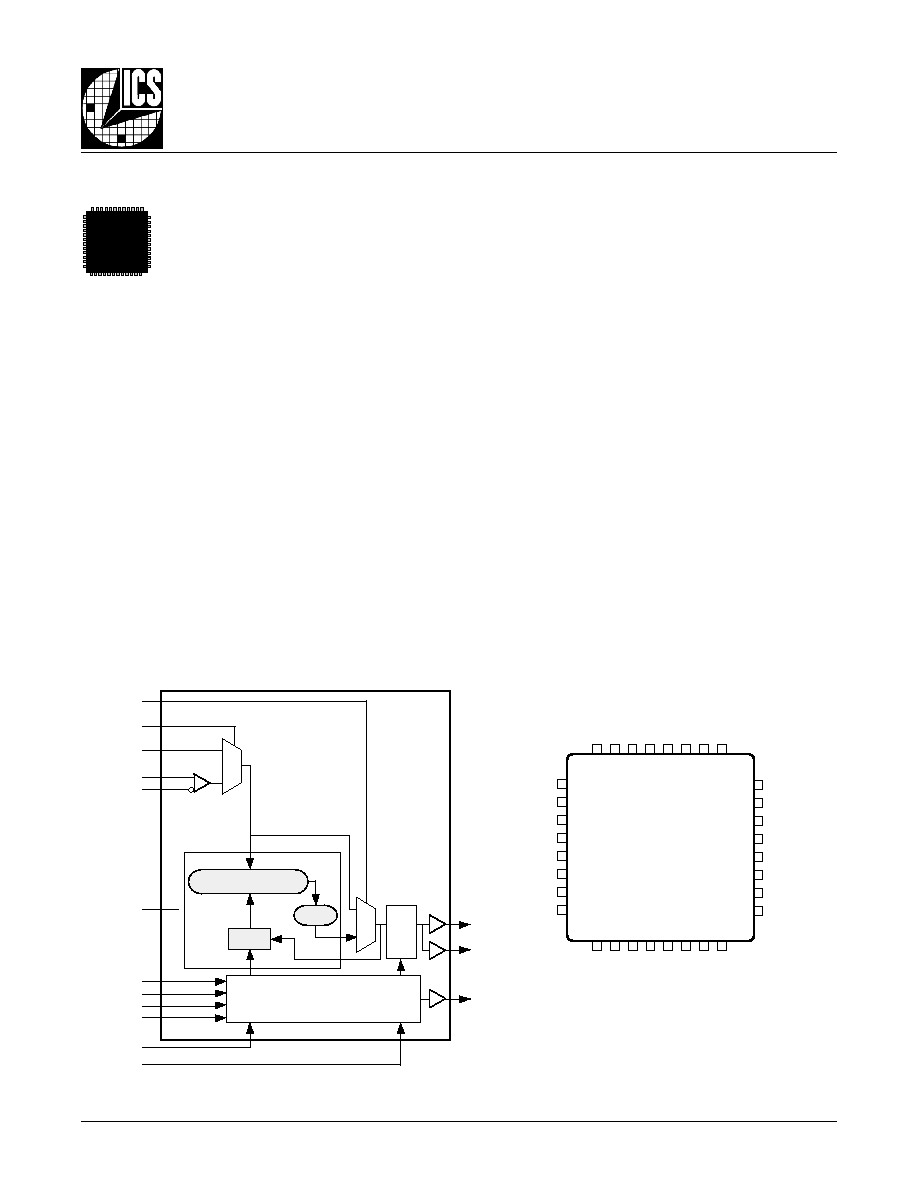
B
LOCK
D
IAGRAM
P
IN
A
SSIGNMENT
F
EATURES
∑
Dual differential 3.3V LVPECL outputs
∑
Selectable CLK, nCLK or LVCMOS/LVTTL TEST_CLK
∑
TEST_CLK can accept the following input levels:
LVCMOS or LVTTL
∑
CLK, nCLK pair can accept the following differential
input levels: LVPECL, LVDS, LVHSTL, SSTL
∑
CLK, nCLK or TEST_CLK maximum input frequency: 40MHz
∑
Output frequency range: 25MHz to 700MHz
∑
VCO range: 200MHz to 700MHz
∑
Accepts any single-ended input signal on CLK input
with resistor bias on nCLK input
∑
Parallel interface for programming counter
and output dividers
∑
RMS period jitter: 5ps (maximum)
∑
Cycle-to-cycle jitter: 25ps (maximum)
∑
3.3V supply voltage
∑
0∞C to 70∞C ambient operating temperature
32 31 30 29 28 27 26 25
9 10 11 12 13 14 15 16
1
2
3
4
5
6
7
8
24
23
22
21
20
19
18
17
CLK
TEST_CLK
CLK_SEL
V
CCA
S_LOAD
S_DATA
S_CLOCK
MR
M5
M6
M7
M8
N 0
N 1
nc
V
EE
V
EE
nFOUT0
FOUT0
V
CCO
nFOUT1
FOUT1
V
CC
TEST
nCLK
nP_LOAD
VCO_SEL
M0
M1
M2
M3
M4
32-Lead LQFP
7mm x 7mm x 1.4mm package body
Y Package
Top View
ICS8432-101
VCO_SEL
CLK_SEL
TEST_CLK
CLK
S_LOAD
S_DATA
S_CLOCK
nP_LOAD
M0:M8
N0:N1
VCO
PLL
FOUT0
nFOUT0
FOUT1
nFOUT1
TEST
CONFIGURATION
INTERFACE
LOGIC
˜
M
0
1
0
1
PHASE DETECTOR
˜
1
˜
2
˜
4
˜
8
MR
nCLK
HiPerClockSTM
,&6

8432DY-101
www.icst.com/products/hiperclocks.html
REV. A FEBRUARY 13, 2003
2
Integrated
Circuit
Systems, Inc.
ICS8432-101
700MH
Z
,
D
IFFERENTIAL
-
TO
-3.3V LVPECL F
REQUENCY
S
YNTHESIZER
F
UNCTIONAL
D
ESCRIPTION
NOTE: The functional description that follows describes operation using a 25MHz clock input. Valid PLL loop divider values
for different input frequencies are defined in the Input Frequency Characteristics, Table 5, NOTE 1.
The ICS8432-101 features a fully integrated PLL and therefore requires no external components for setting the loop bandwidth.
A differential clock input is used as the input to the ICS8432-101. This input is fed into the phase detector.
A 25MHz clock input provides a 25MHz phase detector reference frequency. The VCO of the PLL operates over a range of
200MHz to 700MHz. The output of the M divider is also applied to the phase detector.
The phase detector and the M divider force the VCO output frequency to be M times the reference frequency by adjusting the VCO
control voltage. Note that for some values of M (either too high or too low), the PLL will not achieve lock. The output of the VCO is
scaled by a divider prior to being sent to each of the LVPECL output buffers. The divider provides a 50% output duty cycle.
The programmable features of the ICS8432-101 support two input modes to program the M divider and N output divider. The
two input operational modes are parallel and serial.
Figure 1 shows the timing diagram for each mode. In parallel mode
the nP_LOAD input is initially LOW. The data on inputs M0 through M8 and N0 and N1 is passed directly to the M divider and
N output divider. On the LOW-to-HIGH transition of the nP_LOAD input, the data is latched and the M divider remains loaded
until the next LOW transition on nP_LOAD or until a serial event occurs. As a result, the M and N bits can be hardwired to set
the M divider and N output divider to a specific default state that will automatically occur during power-up. The TEST output is
LOW when operating in the parallel input mode. The relationship between the VCO frequency, the input frequency and the
M divider is defined as follows:
The M value and the required values of M0 through M8 are shown in Table 3B, Programmable VCO Frequency Function Table.
Valid M values for which the PLL will achieve lock for a 25MHz reference are defined as 8
M
28. The frequency out is
defined as follows:
Serial operation occurs when nP_LOAD is HIGH and S_LOAD is LOW. The shift register is loaded by sampling the S_DATA
bits with the rising edge of S_CLOCK. The contents of the shift register are loaded into the M divider and N output divider when
S_LOAD transitions from LOW-to-HIGH. The M divide and N output divide values are latched on the HIGH-to-LOW transition
of S_LOAD. If S_LOAD is held HIGH, data at the S_DATA input is passed directly to the M divider and N output divider on each
rising edge of S_CLOCK. The serial mode can be used to program the M and N bits and test bits T1 and T0. The internal
registers T0 and T1 determine the state of the TEST output as follows:
fVCO = fIN x M
T1
T0
TEST Output
0
0
LOW
0
1
S_Data, Shift Register Input
1
0
Output of M divider
1
1
CMOS Fout
F
IGURE
1. P
ARALLEL
& S
ERIAL
L
OAD
O
PERATIONS
S_CLOCK
S_DATA
S_LOAD
nP_LOAD
M0:M8, N0:N1
nP_LOAD
Time
S
ERIAL
L
OADING
P
ARALLEL
L
OADING
M, N
t
S
t
H
t
S
t
H
t
S
T1
T0
*NULL
N 1
N 0
M8
M7
M6
M5
M4
M3
M2
M1
M0
*NOTE: The NULL timing slot must be observed.
fOUT = fVCO = fIN x M
N
N

8432DY-101
www.icst.com/products/hiperclocks.html
REV. A FEBRUARY 13, 2003
3
Integrated
Circuit
Systems, Inc.
ICS8432-101
700MH
Z
,
D
IFFERENTIAL
-
TO
-3.3V LVPECL F
REQUENCY
S
YNTHESIZER
T
ABLE
1. P
IN
D
ESCRIPTIONS
r
e
b
m
u
N
e
m
a
N
e
p
y
T
n
o
i
t
p
i
r
c
s
e
D
1
5
M
t
u
p
n
I
p
u
ll
u
P
n
o
i
t
s
i
s
n
a
r
t
H
G
I
H
-
o
t
-
W
O
L
n
o
d
e
h
c
t
a
l
a
t
a
D
.
s
t
u
p
n
i
r
e
d
i
v
i
d
M
.
s
l
e
v
e
l
e
c
a
f
r
e
t
n
i
L
T
T
V
L
/
S
O
M
C
V
L
.
t
u
p
n
i
D
A
O
L
_
P
n
f
o
4
,
3
,
2
9
2
,
8
2
2
3
,
1
3
,
0
3
,
8
M
,
7
M
,
6
M
,
1
M
,
0
M
4
M
,
3
M
,
2
M
t
u
p
n
I
n
w
o
d
ll
u
P
6
,
5
1
N
,
0
N
t
u
p
n
I
n
w
o
d
ll
u
P
,
C
3
e
l
b
a
T
n
i
d
e
n
i
f
e
d
s
a
e
u
l
a
v
r
e
d
i
v
i
d
t
u
p
t
u
o
s
e
n
i
m
r
e
t
e
D
.
s
l
e
v
e
l
e
c
a
f
r
e
t
n
i
L
T
T
V
L
/
S
O
M
C
V
L
.
e
l
b
a
T
n
o
i
t
c
n
u
F
7
c
n
d
e
s
u
n
U
.
t
c
e
n
n
o
c
o
N
6
1
,
8
V
E
E
r
e
w
o
P
.
s
n
i
p
y
l
p
p
u
s
e
v
i
t
a
g
e
N
9
T
S
E
T
t
u
p
t
u
O
t
u
p
t
u
O
.
n
o
i
t
a
r
e
p
o
f
o
e
d
o
m
l
a
i
r
e
s
e
h
t
n
i
E
V
I
T
C
A
s
i
h
c
i
h
w
t
u
p
t
u
o
t
s
e
T
.
s
l
e
v
e
l
e
c
a
f
r
e
t
n
i
L
T
T
V
L
/
S
O
M
C
V
L
.
e
d
o
m
l
e
ll
a
r
a
p
n
i
W
O
L
n
e
v
i
r
d
0
1
V
C
C
r
e
w
o
P
.
n
i
p
y
l
p
p
u
s
e
r
o
C
2
1
,
1
1
1
T
U
O
F
n
,
1
T
U
O
F
t
u
p
t
u
O
.
s
l
e
v
e
l
e
c
a
f
r
e
t
n
i
L
C
E
P
V
L
V
3
.
3
.
r
e
z
i
s
e
h
t
n
y
s
e
h
t
r
o
f
t
u
p
t
u
o
l
a
i
t
n
e
r
e
f
f
i
D
3
1
V
O
C
C
r
e
w
o
P
.
n
i
p
y
l
p
p
u
s
t
u
p
t
u
O
5
1
,
4
1
0
T
U
O
F
n
,
0
T
U
O
F
t
u
p
t
u
O
.
s
l
e
v
e
l
e
c
a
f
r
e
t
n
i
L
C
E
P
V
L
V
3
.
3
.
r
e
z
i
s
e
h
t
n
y
s
e
h
t
r
o
f
t
u
p
t
u
o
l
a
i
t
n
e
r
e
f
f
i
D
7
1
R
M
t
u
p
n
I
n
w
o
d
ll
u
P
s
r
e
d
i
v
i
d
l
a
n
r
e
t
n
i
e
h
t
,
H
G
I
H
c
i
g
o
l
n
e
h
W
.
t
e
s
e
R
r
e
t
s
a
M
h
g
i
H
e
v
i
t
c
A
d
e
t
r
e
v
n
i
e
h
t
d
n
a
w
o
l
o
g
o
t
x
T
U
O
F
s
t
u
p
t
u
o
e
u
r
t
e
h
t
g
n
i
s
u
a
c
t
e
s
e
r
e
r
a
s
r
e
d
i
v
i
d
l
a
n
r
e
t
n
i
e
h
t
,
W
O
L
c
i
g
o
l
n
e
h
W
.
h
g
i
h
o
g
o
t
x
T
U
O
F
n
s
t
u
p
t
u
o
d
e
d
a
o
l
t
c
e
f
f
a
t
o
n
s
e
o
d
R
M
f
o
n
o
i
t
r
e
s
s
A
.
d
e
l
b
a
n
e
e
r
a
s
t
u
p
t
u
o
e
h
t
d
n
a
.
s
l
e
v
e
l
e
c
a
f
r
e
t
n
i
L
T
T
V
L
/
S
O
M
C
V
L
.
s
e
u
l
a
v
T
d
n
a
,
N
,
M
8
1
K
C
O
L
C
_
S
t
u
p
n
I
n
w
o
d
ll
u
P
r
e
t
s
i
g
e
r
t
f
i
h
s
e
h
t
o
t
n
i
t
u
p
n
i
A
T
A
D
_
S
t
a
t
n
e
s
e
r
p
a
t
a
d
l
a
i
r
e
s
n
i
s
k
c
o
l
C
.
s
l
e
v
e
l
e
c
a
f
r
e
t
n
i
L
T
T
V
L
/
S
O
M
C
V
L
.
K
C
O
L
C
_
S
f
o
e
g
d
e
g
n
i
s
i
r
e
h
t
n
o
9
1
A
T
A
D
_
S
t
u
p
n
I
n
w
o
d
ll
u
P
e
g
d
e
g
n
i
s
i
r
e
h
t
n
o
d
e
l
p
m
a
s
a
t
a
D
.
t
u
p
n
i
l
a
i
r
e
s
r
e
t
s
i
g
e
r
t
f
i
h
S
.
s
l
e
v
e
l
e
c
a
f
r
e
t
n
i
L
T
T
V
L
/
S
O
M
C
V
L
.
K
C
O
L
C
_
S
f
o
0
2
D
A
O
L
_
S
t
u
p
n
I
n
w
o
d
ll
u
P
.
s
r
e
d
i
v
i
d
e
h
t
o
t
n
i
r
e
t
s
i
g
e
r
t
f
i
h
s
m
o
r
f
a
t
a
d
f
o
n
o
i
t
i
s
n
a
r
t
s
l
o
r
t
n
o
C
.
s
l
e
v
e
l
e
c
a
f
r
e
t
n
i
L
T
T
V
L
/
S
O
M
C
V
L
1
2
V
A
C
C
r
e
w
o
P
.
n
i
p
y
l
p
p
u
s
g
o
l
a
n
A
2
2
L
E
S
_
K
L
C
t
u
p
n
I
p
u
ll
u
P
r
o
t
u
p
n
i
k
c
o
l
c
l
a
i
t
n
e
r
e
f
f
i
d
n
e
e
w
t
e
b
s
t
c
e
l
e
S
.
t
u
p
n
i
t
c
e
l
e
s
k
c
o
l
C
,
H
G
I
H
n
e
h
W
.
e
c
r
u
o
s
e
c
n
e
r
e
f
e
r
L
L
P
e
h
t
s
a
t
u
p
n
i
K
L
C
_
T
S
E
T
.
t
u
p
n
i
K
L
C
_
T
S
E
T
s
t
c
e
l
e
s
,
W
O
L
n
e
h
W
.
s
t
u
p
n
i
K
L
C
n
,
K
L
C
s
t
c
e
l
e
s
.
s
l
e
v
e
l
e
c
a
f
r
e
t
n
i
L
T
T
V
L
/
S
O
M
C
V
L
3
2
K
L
C
_
T
S
E
T
t
u
p
n
I
n
w
o
d
ll
u
P
.
s
l
e
v
e
l
e
c
a
f
r
e
t
n
i
L
T
T
V
L
/
S
O
M
C
V
L
.
t
u
p
n
i
k
c
o
l
c
t
s
e
T
4
2
K
L
C
t
u
p
n
I
n
w
o
d
ll
u
P
.
t
u
p
n
i
k
c
o
l
c
l
a
i
t
n
e
r
e
f
f
i
d
g
n
i
t
r
e
v
n
i
-
n
o
N
5
2
K
L
C
n
t
u
p
n
I
p
u
ll
u
P
.
t
u
p
n
i
k
c
o
l
c
l
a
i
t
n
e
r
e
f
f
i
d
g
n
i
t
r
e
v
n
I
6
2
D
A
O
L
_
P
n
t
u
p
n
I
n
w
o
d
ll
u
P
s
i
0
M
:
8
M
t
a
t
n
e
s
e
r
p
a
t
a
d
n
e
h
w
s
e
n
i
m
r
e
t
e
D
.
t
u
p
n
i
d
a
o
l
l
e
ll
a
r
a
P
e
h
t
s
t
e
s
0
N
:
1
N
t
a
t
n
e
s
e
r
p
a
t
a
d
n
e
h
w
d
n
a
,
r
e
d
i
v
i
d
M
o
t
n
i
d
e
d
a
o
l
.
s
l
e
v
e
l
e
c
a
f
r
e
t
n
i
L
T
T
V
L
/
S
O
M
C
V
L
.
e
u
l
a
v
r
e
d
i
v
i
d
t
u
p
t
u
o
N
7
2
L
E
S
_
O
C
V
t
u
p
n
I
p
u
ll
u
P
.
e
d
o
m
s
s
a
p
y
b
r
o
L
L
P
n
i
s
i
r
e
z
i
s
e
h
t
n
y
s
r
e
h
t
e
h
w
s
e
n
i
m
r
e
t
e
D
.
s
l
e
v
e
l
e
c
a
f
r
e
t
n
i
L
T
T
V
L
/
S
O
M
C
V
L
:
E
T
O
N
p
u
ll
u
P
d
n
a
n
w
o
d
ll
u
P
.
s
e
u
l
a
v
l
a
c
i
p
y
t
r
o
f
,
s
c
i
t
i
s
i
r
e
t
c
a
r
a
h
C
n
i
P
,
2
e
l
b
a
T
e
e
S
.
s
r
o
t
s
i
s
e
r
t
u
p
n
i
l
a
n
r
e
t
n
i
o
t
r
e
f
e
r
T
ABLE
2. P
IN
C
HARACTERISTICS
l
o
b
m
y
S
r
e
t
e
m
a
r
a
P
s
n
o
i
t
i
d
n
o
C
t
s
e
T
m
u
m
i
n
i
M
l
a
c
i
p
y
T
m
u
m
i
x
a
M
s
t
i
n
U
C
N
I
e
c
n
a
t
i
c
a
p
a
C
t
u
p
n
I
4
F
p
R
P
U
L
L
U
P
r
o
t
s
i
s
e
R
p
u
ll
u
P
t
u
p
n
I
1
5
K
R
N
W
O
D
L
L
U
P
r
o
t
s
i
s
e
R
n
w
o
d
ll
u
P
t
u
p
n
I
1
5
K

8432DY-101
www.icst.com/products/hiperclocks.html
REV. A FEBRUARY 13, 2003
4
Integrated
Circuit
Systems, Inc.
ICS8432-101
700MH
Z
,
D
IFFERENTIAL
-
TO
-3.3V LVPECL F
REQUENCY
S
YNTHESIZER
T
ABLE
3A. P
ARALLEL
AND
S
ERIAL
M
ODE
F
UNCTION
T
ABLE
T
ABLE
3B. P
ROGRAMMABLE
VCO F
REQUENCY
F
UNCTION
T
ABLE
T
ABLE
3C. P
ROGRAMMABLE
O
UTPUT
D
IVIDER
F
UNCTION
T
ABLE
s
t
u
p
n
I
s
n
o
i
t
i
d
n
o
C
R
M
D
A
O
L
_
P
n
M
N
D
A
O
L
_
S
K
C
O
L
C
_
S
A
T
A
D
_
S
H
X
X
X
X
X
X
.
W
O
L
s
t
u
p
t
u
o
s
e
c
r
o
F
.
t
e
s
e
R
L
L
a
t
a
D
a
t
a
D
X
X
X
e
h
t
o
t
y
l
t
c
e
r
i
d
d
e
s
s
a
p
s
t
u
p
n
i
N
d
n
a
M
n
o
a
t
a
D
t
u
p
t
u
o
T
S
E
T
.
r
e
d
i
v
i
d
t
u
p
t
u
o
N
d
n
a
r
e
d
i
v
i
d
M
.
W
O
L
d
e
c
r
o
f
L
a
t
a
D
a
t
a
D
L
X
X
d
e
d
a
o
l
s
n
i
a
m
e
r
d
n
a
s
r
e
t
s
i
g
e
r
t
u
p
n
i
o
t
n
i
d
e
h
c
t
a
l
s
i
a
t
a
D
.
s
r
u
c
c
o
t
n
e
v
e
l
a
i
r
e
s
a
li
t
n
u
r
o
n
o
i
t
i
s
n
a
r
t
W
O
L
t
x
e
n
li
t
n
u
L
H
X
X
L
a
t
a
D
n
o
a
t
a
d
h
t
i
w
d
e
d
a
o
l
s
i
r
e
t
s
i
g
e
r
t
f
i
h
S
.
e
d
o
m
t
u
p
n
i
l
a
i
r
e
S
.
K
C
O
L
C
_
S
f
o
e
g
d
e
g
n
i
s
i
r
h
c
a
e
n
o
A
T
A
D
_
S
L
H
X
X
L
a
t
a
D
e
h
t
o
t
d
e
s
s
a
p
e
r
a
r
e
t
s
i
g
e
r
t
f
i
h
s
e
h
t
f
o
s
t
n
e
t
n
o
C
.
r
e
d
i
v
i
d
t
u
p
t
u
o
N
d
n
a
r
e
d
i
v
i
d
M
L
H
X
X
L
a
t
a
D
.
d
e
h
c
t
a
l
e
r
a
s
e
u
l
a
v
r
e
d
i
v
i
d
t
u
p
t
u
o
N
d
n
a
r
e
d
i
v
i
d
M
L
H
X
X
L
X
X
.
s
r
e
t
s
i
g
e
r
t
f
i
h
s
t
c
e
f
f
a
t
o
n
o
d
s
t
u
p
n
i
l
a
i
r
e
s
r
o
l
e
ll
a
r
a
P
L
H
X
X
H
a
t
a
D
.
d
e
k
c
o
l
c
s
i
t
i
s
a
r
e
d
i
v
i
d
M
o
t
y
l
t
c
e
r
i
d
d
e
s
s
a
p
A
T
A
D
_
S
W
O
L
=
L
:
E
T
O
N
H
G
I
H
=
H
e
r
a
c
t
'
n
o
D
=
X
n
o
i
t
i
s
n
a
r
t
e
g
d
e
g
n
i
s
i
R
=
n
o
i
t
i
s
n
a
r
t
e
g
d
e
g
n
il
l
a
F
=
s
t
u
p
n
I
e
u
l
a
V
r
e
d
i
v
i
D
N
)
z
H
M
(
y
c
n
e
u
q
e
r
F
t
u
p
t
u
O
1
N
0
N
m
u
m
i
n
i
M
m
u
m
i
x
a
M
0
0
1
0
0
2
0
0
7
0
1
2
0
0
1
0
5
3
1
0
4
0
5
5
7
1
1
1
8
5
2
5
.
7
8
y
c
n
e
u
q
e
r
F
O
C
V
)
z
H
M
(
e
d
i
v
i
D
M
6
5
2
8
2
1
4
6
2
3
6
1
8
4
2
1
8
M
7
M
6
M
5
M
4
M
3
M
2
M
1
M
0
M
0
0
2
8
0
0
0
0
0
1
0
0
0
5
2
2
9
0
0
0
0
0
1
0
0
1
0
5
2
0
1
0
0
0
0
0
1
0
1
0
5
7
2
1
1
0
0
0
0
0
1
0
1
1
∑
∑
∑
∑
∑
∑
∑
∑
∑
∑
∑
∑
∑
∑
∑
∑
∑
∑
∑
∑
∑
∑
0
5
6
6
2
0
0
0
0
1
1
0
1
0
5
7
6
7
2
0
0
0
0
1
1
0
1
1
0
0
7
8
2
0
0
0
0
1
1
1
0
0
y
c
n
e
u
q
e
r
f
t
u
p
n
i
K
L
C
_
T
S
E
T
r
o
t
u
p
n
i
l
a
i
t
n
e
r
e
f
f
i
d
o
t
d
n
o
p
s
e
r
r
o
c
s
e
i
c
n
e
u
q
e
r
f
g
n
i
t
l
u
s
e
r
e
h
t
d
n
a
s
e
u
l
a
v
e
d
i
v
i
d
M
e
s
e
h
T
:
1
E
T
O
N
.
z
H
M
5
2
f
o

8432DY-101
www.icst.com/products/hiperclocks.html
REV. A FEBRUARY 13, 2003
5
Integrated
Circuit
Systems, Inc.
ICS8432-101
700MH
Z
,
D
IFFERENTIAL
-
TO
-3.3V LVPECL F
REQUENCY
S
YNTHESIZER
T
ABLE
4A. P
OWER
S
UPPLY
DC C
HARACTERISTICS
,
V
CC
= V
CCA
= V
CCO
= 3.3V±5%, T
A
= 0∞C
TO
70∞C
l
o
b
m
y
S
r
e
t
e
m
a
r
a
P
s
n
o
i
t
i
d
n
o
C
t
s
e
T
m
u
m
i
n
i
M
l
a
c
i
p
y
T
m
u
m
i
x
a
M
s
t
i
n
U
V
C
C
e
g
a
t
l
o
V
y
l
p
p
u
S
e
r
o
C
5
3
1
.
3
3
.
3
5
6
4
.
3
V
V
A
C
C
e
g
a
t
l
o
V
y
l
p
p
u
S
g
o
l
a
n
A
5
3
1
.
3
3
.
3
5
6
4
.
3
V
V
O
C
C
e
g
a
t
l
o
V
y
l
p
p
u
S
t
u
p
t
u
O
5
3
1
.
3
3
.
3
5
6
4
.
3
V
I
E
E
t
n
e
r
r
u
C
y
l
p
p
u
S
r
e
w
o
P
0
2
1
A
m
I
A
C
C
t
n
e
r
r
u
C
y
l
p
p
u
S
g
o
l
a
n
A
5
1
A
m
T
ABLE
4B. LVCMOS / LVTTL DC C
HARACTERISTICS
,
V
CC
= V
CCA
= V
CCO
= 3.3V±5%, T
A
= 0∞C
TO
70∞C
l
o
b
m
y
S
r
e
t
e
m
a
r
a
P
s
n
o
i
t
i
d
n
o
C
t
s
e
T
m
u
m
i
n
i
M
l
a
c
i
p
y
T
m
u
m
i
x
a
M
s
t
i
n
U
V
H
I
t
u
p
n
I
e
g
a
t
l
o
V
h
g
i
H
,
R
M
,
L
E
S
_
K
L
C
,
L
E
S
_
O
C
V
,
A
T
A
D
_
S
,
D
A
O
L
_
S
,
D
A
O
L
_
P
n
,
K
C
O
L
C
_
S
1
N
:
0
N
,
8
M
:
0
M
2
V
C
C
3
.
0
+
V
K
L
C
_
T
S
E
T
2
V
C
C
3
.
0
+
V
V
L
I
t
u
p
n
I
e
g
a
t
l
o
V
w
o
L
,
R
M
,
L
E
S
_
K
L
C
,
L
E
S
_
O
C
V
,
A
T
A
D
_
S
,
D
A
O
L
_
S
,
D
A
O
L
_
P
n
,
K
C
O
L
C
_
S
1
N
:
0
N
,
8
M
:
0
M
3
.
0
-
8
.
0
V
K
L
C
_
T
S
E
T
3
.
0
-
3
.
1
V
I
H
I
t
u
p
n
I
t
n
e
r
r
u
C
h
g
i
H
,
R
M
,
1
N
,
0
N
,
8
M
-
6
M
,
4
M
-
0
M
,
K
L
C
_
T
S
E
T
,
K
C
O
L
C
_
S
D
A
O
L
_
P
n
,
D
A
O
L
_
S
,
A
T
A
D
_
S
V
C
C
V
=
N
I
V
5
6
4
.
3
=
0
5
1
A
µ
L
E
S
_
O
C
V
,
L
E
S
_
K
L
C
,
5
M
V
C
C
V
=
N
I
V
5
6
4
.
3
=
5
A
µ
I
L
I
t
u
p
n
I
t
n
e
r
r
u
C
w
o
L
,
R
M
,
1
N
,
0
N
,
8
M
-
6
M
,
4
M
-
0
M
,
K
L
C
_
T
S
E
T
,
K
C
O
L
C
_
S
D
A
O
L
_
P
n
,
D
A
O
L
_
S
,
A
T
A
D
_
S
V
C
C
,
V
5
6
4
.
3
=
V
N
I
V
0
=
5
-
A
µ
L
E
S
_
O
C
V
,
L
E
S
_
K
L
C
,
5
M
V
C
C
,
V
5
6
4
.
3
=
V
N
I
V
0
=
0
5
1
-
A
µ
V
H
O
t
u
p
t
u
O
e
g
a
t
l
o
V
h
g
i
H
T
S
E
T
V
C
C
,
V
5
3
1
.
3
=
I
H
O
A
m
6
3
-
=
6
.
2
V
V
L
O
t
u
p
t
u
O
e
g
a
t
l
o
V
w
o
L
T
S
E
T
V
C
C
,
V
5
3
1
.
3
=
I
L
O
A
m
6
3
=
5
.
0
V
A
BSOLUTE
M
AXIMUM
R
ATINGS
Supply Voltage, V
CC
4.6V
Inputs, V
I
-0.5V to V
CC
+ 0.5 V
Outputs, V
O
-0.5V to V
CCO
+ 0.5V
Package Thermal Impedance,
JA
47.9∞C/W (0 lfpm)
Storage Temperature, T
STG
-65∞C to 150∞C
NOTE: Stresses beyond those listed under Absolute
Maximum Ratings may cause permanent damage to the
device. These ratings are stress specifications only. Functional
operation of product at these conditions or any conditions be-
yond those listed in the
DC Characteristics or AC Character-
istics is not implied. Exposure to absolute maximum rating
conditions for extended periods may affect product reliability.