8602BY
www.icst.com/products/hiperclocks.html
REV. E OCTOBER 9, 2002
1
Integrated
Circuit
Systems, Inc.
ICS8602
Z
ERO
D
ELAY
, D
IFFERENTIAL
-
TO
-LVCMOS
C
LOCK
G
ENERATOR
PRELIMINARY
G
ENERAL
D
ESCRIPTION
The ICS8602 is a high performance, low skew,
1-to-9 Differential-to-LVCMOS zero delay buffer
and a member of the HiPerClockSTM family of
High Performance Clocks Solutions from ICS.
The CLK, nCLK pair can accept most standard
differential input levels. The VCO operates at a frequency range
of 200MHz to 500MHz. The external feedback allows the de-
vice to achieve "zero delay" between the input clock and the
output clocks. The PLL_SEL pin can be used to bypass the
PLL for system test and debug purposes. In bypass mode,
the reference clock is routed around the PLL and into the in-
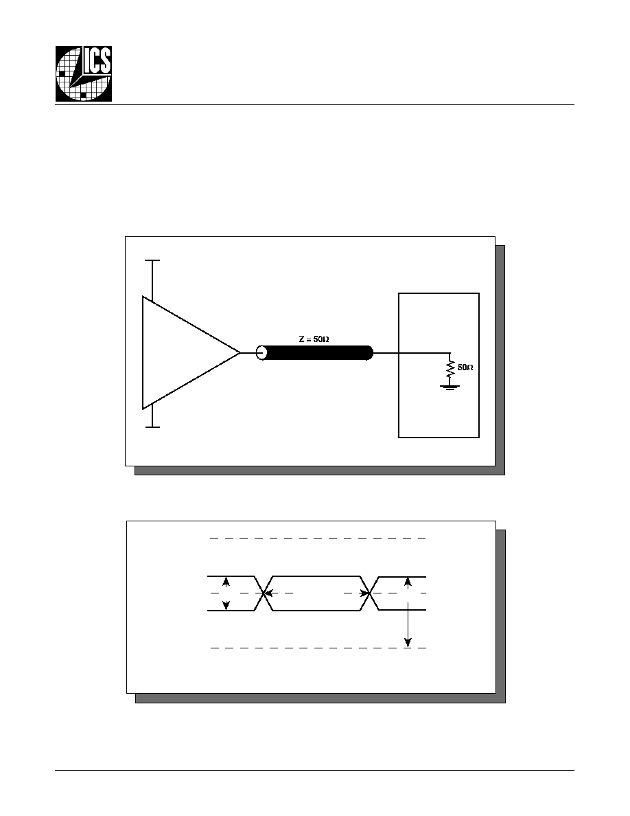
ternal output dividers.The low impedance LVCMOS outputs
are designed to drive 50
series or parallel terminated trans-
mission lines. The effective fanout can be doubled by utilizing
the ability of the outputs to drive two series terminated lines.
The differential reference clock input will accept any differen-
tial signal levels.
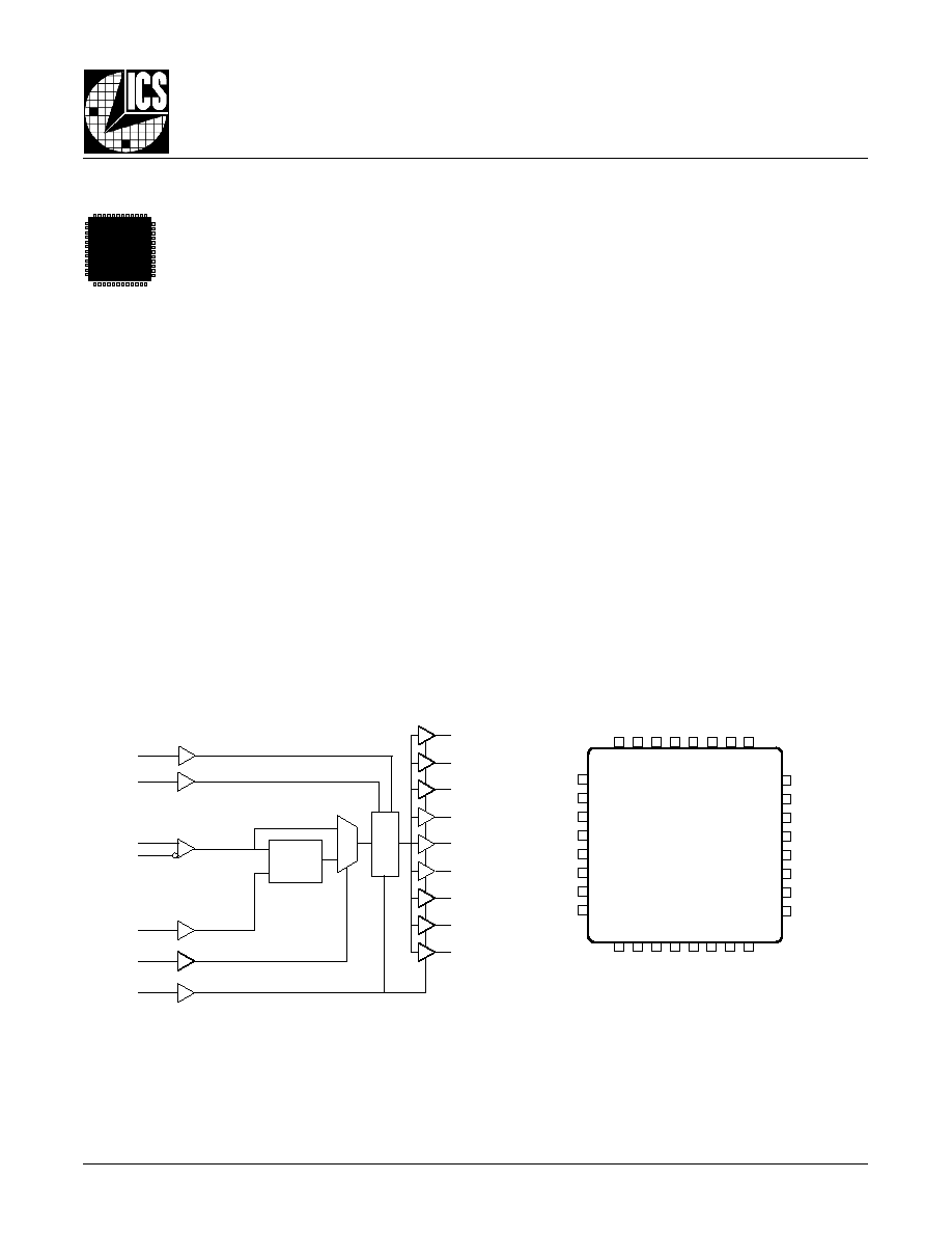
B
LOCK
D
IAGRAM
P
IN
A
SSIGNMENT
F
EATURES
·
Fully integrated PLL
·
9 LVCMOS outputs, 7
typical output impedance
·
CLK, nCLK pair can accept the following differential
input levels: LVDS, LVPECL, LVHSTL, SSTL, HCSL
·
Output frequency range: 12.5MHz to 250MHz
·
Input frequency range: 12.5MHz to 250MHz
· VCO range: 200MHz to 500MHz
· External feedback for "zero delay" clock regeneration
with configurable frequencies
· Cycle-to-cycle jitter: 36ps (typical)
· Output skew: 125ps (maximum)
· Static Phase Offset: TBD±100ps (typical)
· 3.3V supply voltage
· 0°C to 70°C ambient operating temperature
32 31 30 29 28 27 26 25
9 10 11 12 13 14 15 16
1
2
3
4
5
6
7
8
24
23
22
21
20
19
18
17
V
DDO
Q5
GND
Q4
V
DDO
Q3
GND
MR / nOE
V
DDA
V
DD
CLK
nCLK
GND
DIV_SEL0
DIV_SEL1
GND
GND
Q2
V
DDO
Q1
GND
Q0
V
DDO
FB_IN
GND
Q6
V
DDO
Q7
GND
Q8
V
DDO
PLL_SEL
32-Lead LQFP
7mm x 7mm x 1.4mm package body
Y Package
Top View
ICS8602
The Preliminary Information presented herein represents a product in prototyping or pre-production. The noted characteristics are based on initial
product characterization. Integrated Circuit Systems, Incorporated (ICS) reserves the right to change any circuitry or specifications without notice.
HiPerClockSTM
,&6
Q0
Q1
Q2
Q3
Q4
Q5
Q6
Q7
Q8
SEL0
SEL1
CLK
nCLK
FB_IN
PLL_SEL
MR / nOE
0
1
PLL
÷2
÷4
÷8
÷16
8602BY
www.icst.com/products/hiperclocks.html
REV. E OCTOBER 9, 2002
3
Integrated
Circuit
Systems, Inc.
ICS8602
Z
ERO
D
ELAY
, D
IFFERENTIAL
-
TO
-LVCMOS
C
LOCK
G
ENERATOR
PRELIMINARY
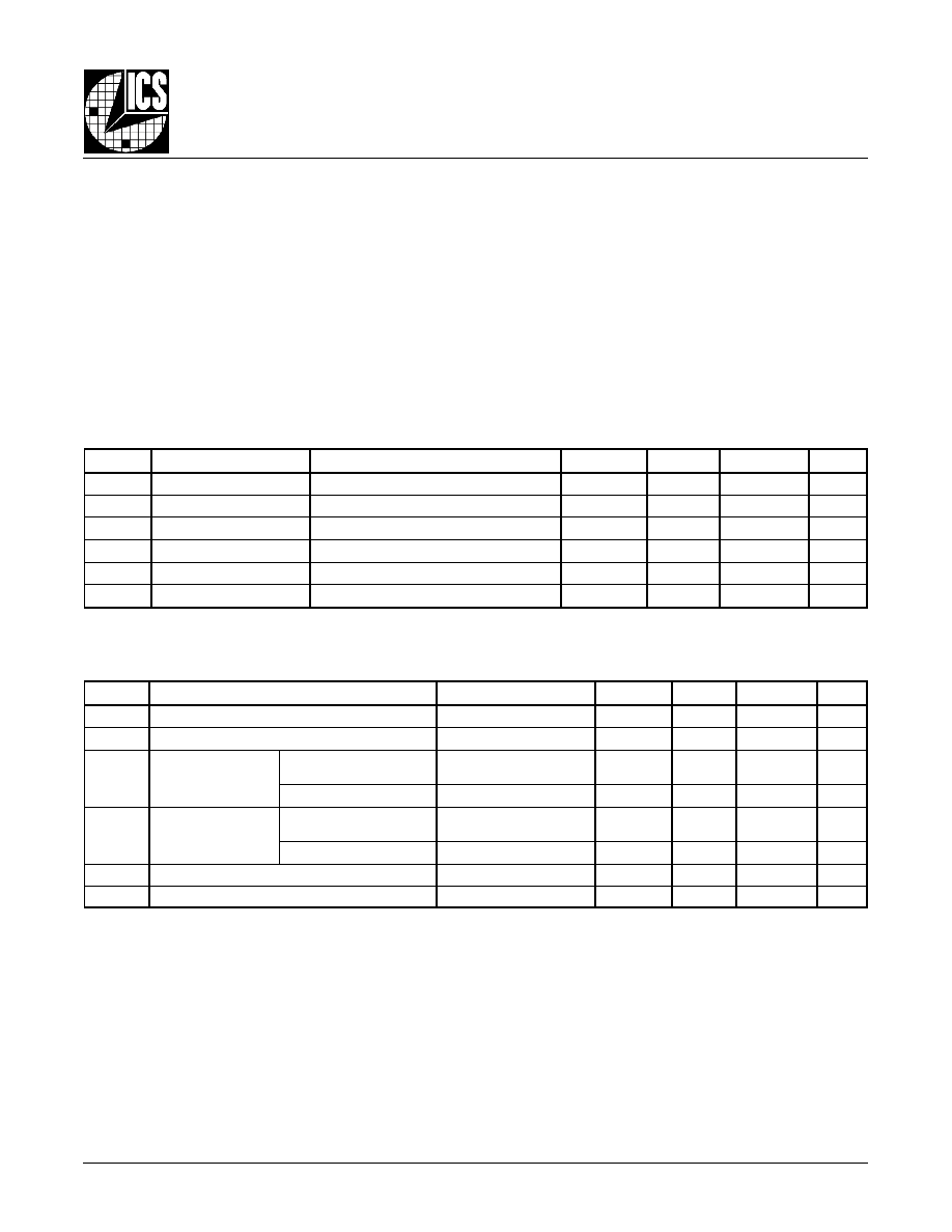
T
ABLE
4B. LVCMOS / LVTTL DC C
HARACTERISTICS
,
V
DD
= V
DDA
= V
DDO
= 3.3V±5%, T
A
= 0°C
TO
70°C
T
ABLE
4A. P
OWER
S
UPPLY
DC C
HARACTERISTICS
,
V
DD
= V
DDA
= V
DDO
= 3.3V±5%, T
A
= 0°C
TO
70°C
A
BSOLUTE
M
AXIMUM
R
ATINGS
Supply Voltage, V
DDx
4.6V
Inputs, V
I
-0.5V to V
DD
+ 0.5 V
Outputs V
O
-0.5V to V
DDO
+ 0.5V
Ambient Operating Temperature 42.1°C (0 lfpm)
Storage Temperature
-65°C to 150°C
Stresses beyond those listed under Absolute Maximum Ratings may cause permanent damage to the device. These ratings are
stress specifications only. Functional operation of product at these conditions or any conditions beyond those listed in the
DC
Characteristics or AC Characteristics is not implied. Exposure to absolute maximum rating conditions for extended periods may
affect product reliability.
l
o
b
m
y
S
r
e
t
e
m
a
r
a
P
s
n
o
i
t
i
d
n
o
C
t
s
e
T
m
u
m
i
n
i
M
l
a
c
i
p
y
T
m
u
m
i
x
a
M
s
t
i
n
U
V
H
I
e
g
a
t
l
o
V
h
g
i
H
t
u
p
n
I
2
V
D
D
3
.
0
+
V
V
L
I
e
g
a
t
l
o
V
w
o
L
t
u
p
n
I
3
.
0
-
8
.
0
V
I
H
I
t
n
e
r
r
u
C
h
g
i
H
t
u
p
n
I
,
1
L
E
S
_
V
I
D
,
0
L
E
S
_
V
I
D
E
O
n
/
R
M
,
N
I
_
B
F
V
D
D
V
=
N
I
V
5
6
4
.
3
=
0
5
1
A
µ
L
E
S
_
L
L
P
V
D
D
V
=
N
I
V
5
6
4
.
3
=
5
A
µ
I
L
I
t
n
e
r
r
u
C
w
o
L
t
u
p
n
I
,
1
L
E
S
_
V
I
D
,
0
L
E
S
_
V
I
D
E
O
n
/
R
M
,
N
I
_
B
F
V
D
D
V
,
V
5
6
4
.
3
=
N
I
V
0
=
5
-
A
µ
L
E
S
_
L
L
P
V
D
D
V
,
V
5
6
4
.
3
=
N
I
V
0
=
0
5
1
-
A
µ
V
H
O
1
E
T
O
N
;
e
g
a
t
l
o
V
h
g
i
H
t
u
p
t
u
O
6
.
2
V
V
L
O
1
E
T
O
N
;
e
g
a
t
l
o
V
w
o
L
t
u
p
t
u
O
5
.
0
V
0
5
h
t
i
w
d
e
t
a
n
i
m
r
e
t
s
t
u
p
t
u
O
:
1
E
T
O
N
V
o
t
O
D
D
,
n
o
i
t
a
m
r
o
f
n
I
t
n
e
m
e
r
u
s
a
e
M
r
e
t
e
m
a
r
a
P
e
e
S
.
2
/
.
t
i
u
c
r
i
C
t
s
e
T
d
a
o
L
t
u
p
t
u
O
V
3
.
3
l
o
b
m
y
S
r
e
t
e
m
a
r
a
P
s
n
o
i
t
i
d
n
o
C
t
s
e
T
m
u
m
i
n
i
M
l
a
c
i
p
y
T
m
u
m
i
x
a
M
s
t
i
n
U
V
D
D
e
g
a
t
l
o
V
y
l
p
p
u
S
e
r
o
C
5
3
1
.
3
3
.
3
5
6
4
.
3
V
V
A
D
D
e
g
a
t
l
o
V
y
l
p
p
u
S
g
o
l
a
n
A
5
3
1
.
3
3
.
3
5
6
4
.
3
V
V
O
D
D
e
g
a
t
l
o
V
y
l
p
p
u
S
t
u
p
t
u
O
5
3
1
.
3
3
.
3
5
6
4
.
3
V
I
D
D
t
n
e
r
r
u
C
y
l
p
p
u
S
r
e
w
o
P
0
4
A
m
I
A
D
D
t
n
e
r
r
u
C
y
l
p
p
u
S
g
o
l
a
n
A
0
1
A
m
I
O
D
D
t
n
e
r
r
u
C
y
l
p
p
u
S
t
u
p
t
u
O
0
6
1
A
m