Integrated
Circuit
Systems, Inc.
General Description
Features
AV9107C-17
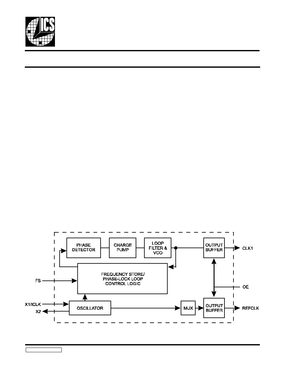
Block Diagram
CPU Frequency Generator
Applications
Computer: The AV9107C-17 is the ideal solution for
replacing high speed oscillators and for reducing clock
speeds to save power in computers. The device provides
smooth, glitch-free frequency transitions so that the CPU
can continue to operate during slow down or speed up. The
rate of frequency change makes the AV9107C-17
compatible with all 386DX, 386SX, 486DX, 486DX2, and
486SX devices.
AV 9107-17 RevC052197P
The AV9107C-17 offers a tiny footprint solution for
generating two simultaneous clocks. One clock, the
REFCLK, is a fixed output frequency which is the same as
the input reference crystal (or clock). The other clock,
CLK1, can vary between 25.06 and 33.29 MHz.
The device has advanced features which include on-chip
loop filters, tristate outputs, and power-down capability. A
mini-mum of external components - two decoupling
capacitors and an optional ferrite bead - are all that are
required for jitter-free operation.
Patented on-chip Phase-Locked Loop with VCO
for clock generation
Provides reference clock and synthesized clock
Generates frequencies of 25 and 33 MHz
8-pin DIP or SOIC package
14.318 MHz input reference frequency
On-chip loop filter
Low power CMOS technology
Single +3.3 or +5 volt power supply
∑
∑
∑
∑
∑
∑
∑
∑

2
AV9107C-17
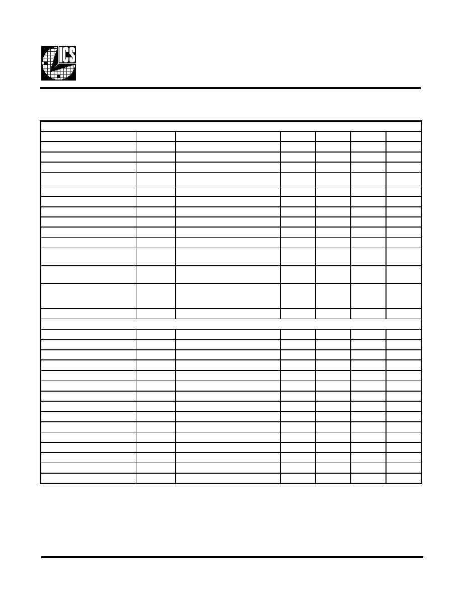
Pin Descriptions
Pin Configuration
8-Pin DIP, SOIC
Functionality
(at 14.318) MHz reference frequency input)
Frequency Transitions
A key AV9107C-17 feature is the ability to provide glitch-
free frequency transitions between its output frequencies.
Output Enable
The Output Enable feature tristates the specified output
clock pins. This places the selected output pin in a high
impedance state to allow for system level diagnostic testing.
Absolute Maximum Ratings
AVDD, VDD referenced to GND . . . . . . . . . . . . . . . 7V
Operating temperature under bias. . . . . . . . . . . . . . . . 0∞C to +70∞C
Storage temperature . . . . . . . . . . . . . . . . . . . . . . . . . . -65∞C to +150∞C
Voltage on I/O pins referenced to GND. . . . . . . . . . . GND -0.5V to VDD +0.5V
Power dissipation . . . . . . . . . . . . . . . . . . . . . . . . . . . . 0.5 Watts
Stresses above those listed under Absolute Maximum Ratings may cause permanent damage to the device.
This is a stress rating only and functional operation of the device at these or any other conditions above
those indicated in the operational sections of the specifications is not implied. Exposure to absolute
maximum rating conditions for extended periods may affect product reliability.
FS
CLK1
0
1
25.06 MHz
33.29 MHz
PIN
NUMBER
PIN NAME
TYPE
DESCRIPTION
1
FS0
Input
Frequency Select 0 for CLK1.
2
GND
-
Digital Ground.
3
X1/ICLK
Input
Crystal Output or Input Clock frequency. Typically 14.318 MHz system clock.
4
X2
Output
Crystal Output (No Connect when clock used.).
5
OE
Input
Output Enable. Tristates CLK1 and REFCLK when low. Has internal pull-up.
6
CLK1
Output
Clock 1 Output (see decoding tables).
7
VDD
-
Digital power supply (+5V DC).
8
REFCLK
Output
Reference Clock output. Produces a buffered version of the input clock or crystal frequency
(typically 14.318 MHz).
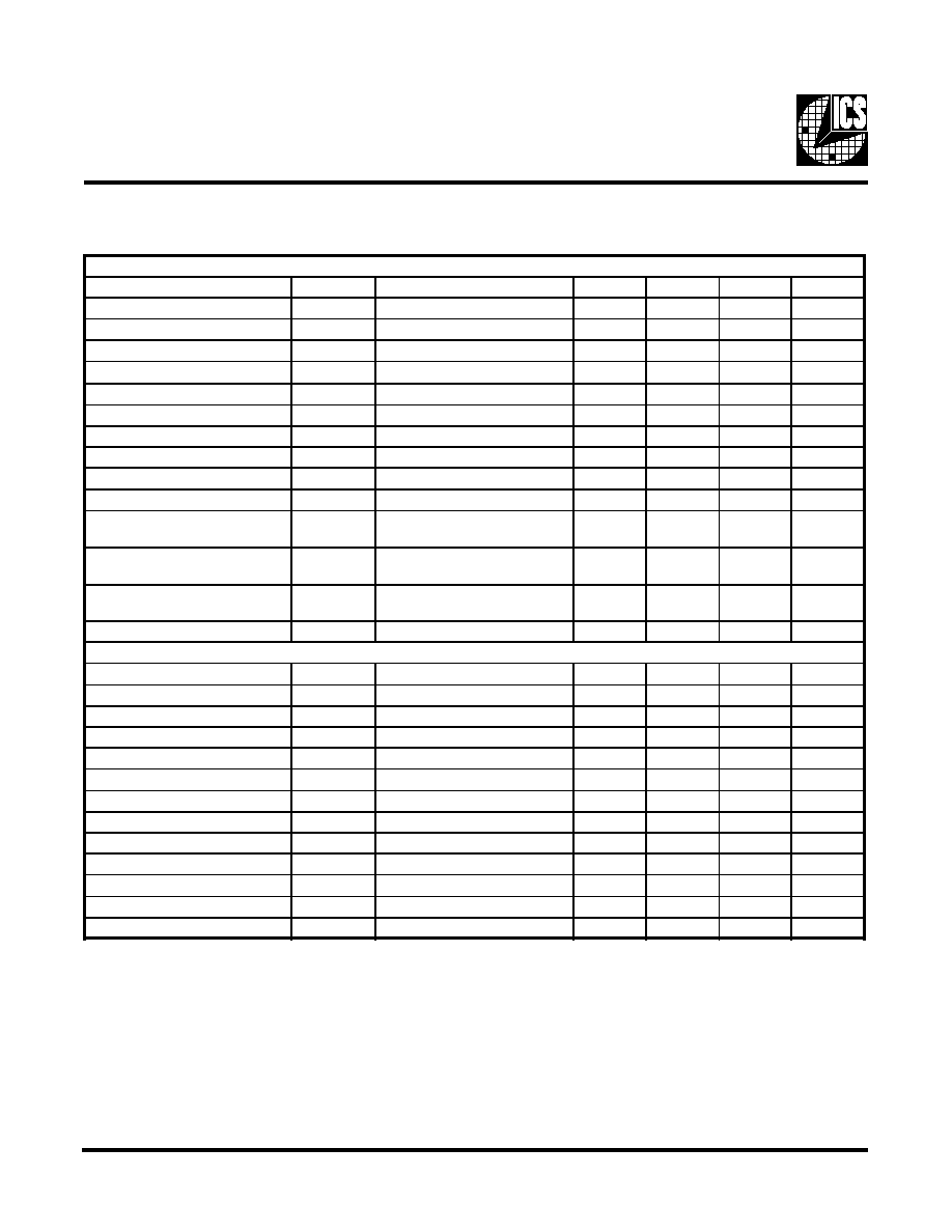
3
AV9107C-17
Note 1:
Parameter is guaranteed by design and characterization. Not 100% tested in production.
Electrical Characteristics at 5.0V
Operating V
DD
= +4.5V to +5.5V; T
A
=0∞C to 70∞C unless otherwise stated
DC Characteristics
PARAMETER
SYMBOL
TEST CONDITIONS
MIN
TYP
MAX
UNITS
Input Low Voltage
V
IL
-
-
0.8
V
Input High Voltage
V
IH
2.0
-
-
V
Input Low Current
I
IL
V
IN
=0V (Pull-up input)
-
6.0
16.0
µA
Input Low Current
I
IL
V
IN
=0V (Input with no pull-up)
-2.0
2.0
µA
Input High Current
I
IH
V
IN
=V
DD
-2.0
-
2.0
µA
Output Low Voltage, Note 1
V
OL
I
OL
=10mA
-
0.15
0.40
V
Output High Voltage, Note 1
V
OH
I
OH
=-30mA
2.4
3.25
-
V
Output Low Current, Note 1
I
OL
V
OL
=0.8V
22.0
35.0
-
mA
Output High Current, Note 1
I
OH
V
OH
=2.0V
-
-50.0
-35.0
mA
Supply Current
I
DD
Unload, 50 Mhz
-
18.0
42.0
mA
Supply Current; Power-down
(-03 only)
I
DD
(PD low)
Unload, Logic Inputs 000
-
38.0
100.0
µA
Supply Current; Power-down
(-03 only)
I
DD
(PD low)
Unload, Logic Inputs 111
-
14.0
40.0
µA
Supply Current; Slow Clock
(-11 only)
I
DD
(Slow
Clock low)
Unloaded, Slow Clock pin low
-
5.5
9.0
µA
Pull-up Resistor, Note 1
R
pu
-
380.0
700.0
k ohms
AC Characteristics
Rise Time 0.8 to 2.0V, Note 1
T
r
15pF load
-
0.60
1.40
ns
Fall Time 2.0 to 0.8V, Note 1
T
f
15pF load
-
0.40
1.00
ns
Rise Time 20% to 80%, Note 1
T
r
15pF load
-
2.0
3.5
ns
Fall Time 80% to 20%, Note 1
T
f
15pF load
-
1.0
2.5
ns
Duty Cycle, Note 1
D
t
15pF load @1.4V
45.0
50.0
55.0
%
Jitter, One Sigma, Note 1
T
jis
From 20 to 100 Mhz
-
50.0
150.0
ps
Jitter, One Sigma, Note 1
T
jis
From 14 to 16 Mhz
100.0
200.0
ps
Jitter, One Sigma, Note 1
T
jis
From 14 to Below
0.2
1.0
%
Jitter, Absolute, Note 1
T
jab
From 20 to 100 Mhz
-250.0
250.0
ps
Jitter, Absolute, Note 1
T
jab
From 14 to 16 Mhz
-500.0
500.0
ps
Jitter, Absolute, Note 1
T
jab
From 14 to Below
1.0
3.0
%
Input Frequency, Note 1
F
i
11.0
14.3
19.0
MHz
Output Frequency
F
o
2.0
-
120.0
MHz
Power-up Time, Note 1
T
pu
-
7.58
18.0
ms
Transition Time, Note 1
T
ft
25 to 33.3 Mhz
-
6.0
13.0
ms
4
AV9107C-17
Electrical Characteristics at 3.3V
Note 1:
Parameter is guaranteed by design and characterization. Not 100% tested in production.
Operating V
DD
= +3.0V to +3.7V; T
A
=0∞C to 70∞C unless otherwise stated
DC Characteristics
PARAMETER
SYMBOL
TEST CONDITIONS
MIN
TYP
MAX
UNITS
Input Low Voltage
V
IL
-
-
0.20V
DD
V
Input High Voltage
V
IH
0.7VDD
-
-
V
Input Low Current
I
IL
V
IN
=0V (Pull-up input)
-
2.5
7.0
µA
Input Low Current
I
IL
V
IN
=0V (Input with no pull-up)
-2.0
2.0
µA
Input High Current
I
IH
V
IN
=V
DD
-2.0
-
2.0
µA
Output Low Voltage, Note 1
V
OL
I
OL
=6mA
-
0.15
0.1
V
Output High Voltage, Note 1
V
OH
I
OH
=-5mA
0.85
0.92
-
V
Output Low Current, Note 1
I
OL
V
OL
=0.2V
DD
15.0
22.0
-
mA
Output High Current, Note 1
I
OH
V
OL
=0.7V
DD
-
-17.0
-10.0
mA
Supply Current
I
DD
Unloaded, 50 Mhz
-
22.0
40.0
mA
Supply Current; Power-down
(-03 only)
I
DD
(PD
low)
Unload, Logic Inputs 000
-
13.0
40.0
µA
Supply Current; Power-down
(-03 only)
I
DD
(PD
low)
Unload, Logic Inputs 111
-
4.0
12.0
µA
Supply Current; Slow Clock
(-11 only)
I
DD
(Slow
Clock low)
Unloaded, Slow Clock pin low
-
3.5
6.0
mA
Pull-up Resistor
Rpu
-
550.0
900.0
k ohms
AC Characteristics
Rise Time 20% to 80%, Note 1
T
r
15pF load
-
2.2
3.5
ns
Fall Time 80% to 20%, Note 1
T
f
15pF load
-
1.2
2.5
ns
Duty Cycle, Note 1
D
t
15pF load @ 50%
40.0
46.0
53.0
%
Jitter, One Sigma, Note 1
T
jis
From 25 to 66 Mhz
-
50.0
150.0
ps
Jitter, One Sigma, Note 1
T
jis
From 14 to 20 Mhz
100.0
200.0
ps
Jitter, One Sigma, Note 1
T
jis
From 14 to Below
0.4
1.0
%
Jitter, Absolute, Note 1
T
jab
From 25 to 66 Mhz
-250.0
250.0
ps
Jitter, Absolute, Note 1
T
jab
From 14 to 20 Mhz
-500.0
500.
ps
Jitter, Absolute, Note 1
T
jab
From 14 to Below
1.0
3.0
%
Input Frequency, Note 1
F
i
13.3
14.3
15.3
MHz
Output Frequency, Note 1
F
o
2.0
-
66.6
MHz
Power-up Time, Note 1
T
pu
-
7.58
18.0
ms
Transition Time, Note 1
T
ft
25 to 33.3 Mhz
-
6.0
13.0
ms

5
AV9107C-17
Ordering Information
AV9107C-17CN08 or AV9107C-17CS08
Example:
XXX XXXX-PPP M X#W
8-Pin Plastic SOIC Package
Lead Count & Package Width
Lead Count=1, 2 or 3 digits
W=.3" SOIC or .6" DIP; None=Standard Width
Package Type
N=DIP (Plastic)
S=SOIC
Pattern Number (2 or 3 digit number for parts with ROM code patterns, if applicable)
Device Type (consists of 3 or 4 digit numbers)
Prefix
ICS, AV=Standard Device; GSP=Genlock Device
8-Pin DIP Package