Integrated
Circuit
Systems, Inc.
General Description
Features
AV9155
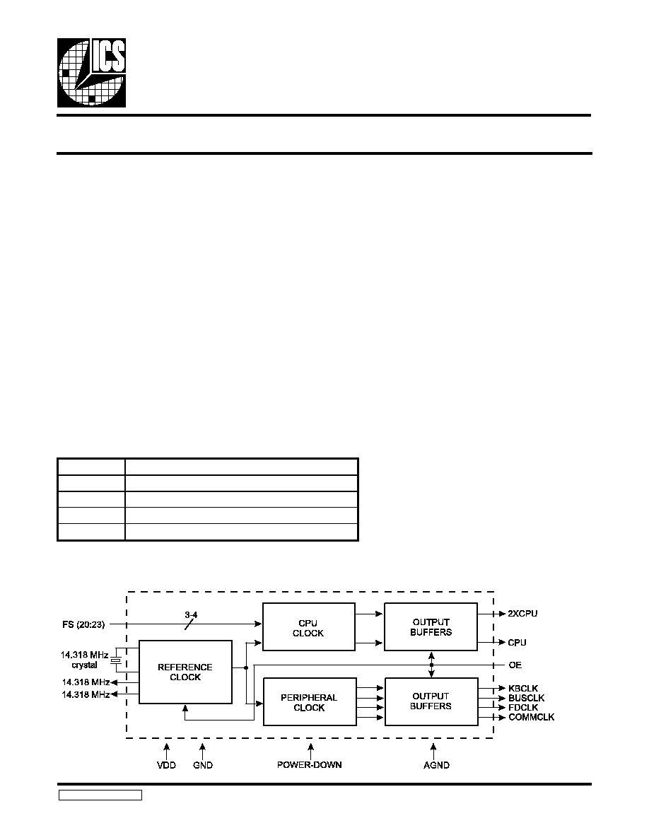
Block Diagram
9155 Rev B 8/24/98
Low Cost 20-Pin Frequency Generator
The AV9155 is a low cost frequency generator designed spe-
cifically for desktop and notebook PC applications. Its CPU
clocks provide all necessary CPU frequencies for 286, 386 and
486 systems, including support for the latest speeds of proces-
sors. The device uses a 14.318 MHz crystal to generate the
CPU and all peripheral clocks for integrated desktop
motherboards.
The dual 14.318 MHz clock outputs allows one output for the
system and one to be the input to an ICS graphics frequency
generator such as the AV9194.
The CPU clock offers the unique feature of smooth, glitch-free
transitions from one frequency to the next, making this ideal
device to use whenever slowing the CPU speed. The AV9155
makes a gradual transition between frequencies, so that it
obeys the Intel cycle-to-cycle timing specification for 486
systems. The simultaneous 2X and 1X CPU clocks offer
controlled skew to within 1.5ns (max) of each other.
ICS offers several versions of the AV9155. The different devices
are shown below:
Compatible with 286, 386, and 486 CPUs
Supports turbo modes
Generates communications clock, keyboard clock,
floppy disk clock, system reference clock, bus clock
and CPU clock
Output enable tristates outputs
Up to 100 MHz at 5V or 3.3V
20-pin DIP or SOIC
All loop filter components internal
Skew-controlled 2X and 1X CPU clocks
Power-down option
ICS has been shipping motherboard frequency generators
since April 1990, and is the leader in the area of multiple output
clocks on a single chip. The AV9155 is a third generation
device, and uses ICSs patented analog CMOS phase-locked
loop technology for low phase jitter. ICS offers a broad family
of frequency generators for motherboards, graphics and other
applications, including cost-effective versions with only one
or two output clocks. Consult ICS for all of your clock
generation needs.
Pentium is a trademark of Intel Corporation.
PART
DESCRIPTION
AV9155C-01
Motherboard clock generator with 16 MHz BUS CLK
AV9155C-02
Motherboard clock generator with 32 MHz BUS CLK
AV9155C-23
Includes Pentium
TM
frequencies
AV9155C-36
Features a special 40 MHz SCSI clock
2
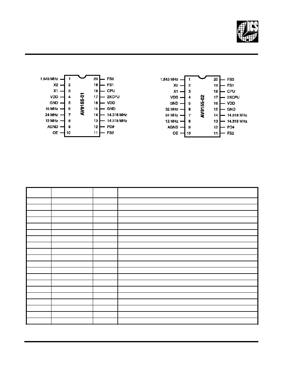
AV9155
Pin Configuration
20-Pin DIP or SOIC
20-Pin DIP or SOIC
Pin Descriptions for AV 9155-01, 9155-02
PIN
N UM BER
PIN N AM E
TYPE
DESC RIPTIO N
1
1.843 M Hz
O utput
1.84 M Hz clock output.
2
X2
O utput
C rystal connection.
3
X1
Input
C rystal connection.
4
VDD
-
Digital power supply (3.3V or 5.0V).
5
GN D
-
Digital Ground.
6
16 M Hz/32 M Hz
O utput
16 M Hz (-01) or 32 M Hz (-02) clock output.
7
24 M Hz
O utput
24 M Hz floppy disk/combination I/O clock output.
8
12 M Hz
O utput
12 M Hz keyboard clock output.
9
AGN D
-
Analog ground (original version).
10
O E
Input
O utput enable. Tristates all outputs when low. (Has internal pull-up.)
11
FS2
Input
C PU clock frequency select #2. (Has internal pull-up.)
12
PD#
Input
Power-down. Shuts off entire chip when low. (Has internal pull-up.)
13
14.318 M Hz
O utput
14.318 M Hz reference clock output.
14
14.318 M Hz
O utput
14.318 M Hz reference clock output.
15
GN D
-
Digital ground.
16
VDD
-
Digital power supply (3.3V or 5.0V).
17
2XC PU
O utput
2X C P U clock output.
18
C PU
O utput
1X C PU clock output.
19
FS1
Input
C PU clock frequency select #1. (Has internal pull-up.)
20
FS0
Input
C PU clock frequency select #0. (Has internal pull-up.)

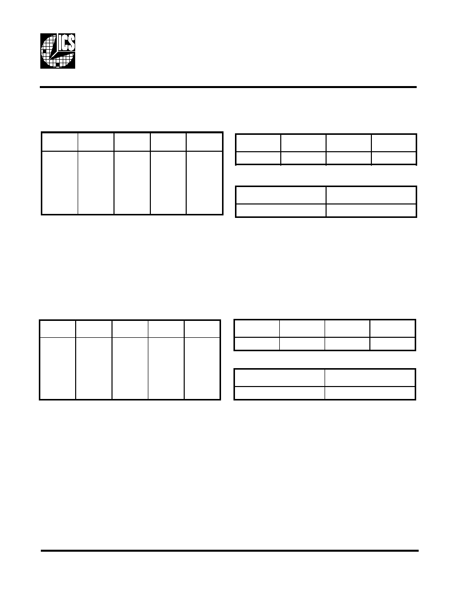
3
AV9155
Functionality
- AV9155-01
(Using 14.318 MHz input. All frequencies in MHz.)
CLOCK#2 CPU and 2XCPU
*5V only.
PERIPHERAL CLOCKS
REFERENCE CLOCKS
Functionality - AV9155-02
(Using 14.318 MHz input. All frequencies in MHz.)
CLOCK#2 CPU and 2XCPU
PERIPHERAL CLOCKS
REFERENCE CLOCKS
Frequency Transitions
A key feature of the AV9155 is its ability to provide smooth,
glitch-free frequency transitions on the CPU and 2XCPU clocks
when the frequency select pins are changed. These frequency
transitions do not violate the Intel 486 specification of less
than 0.1% frequency change per clock period.
Using an Input Clock as Reference
The AV9155 is designed to accept a 14.318 MHz crystal as the
input reference. With some external changes, it is possible to
use a crystal oscillator or clock input. Please see application
note AN04 for details on driving the AV9155 with a clock.
COMMCLK
(Pin 1)
BUSCLK
(Pin 6)
FDCLK
(Pin 7)
KBCLK
(Pin 8)
1.843*
16*
24*
12*
COMMCLK
(Pin 1)
BUSCLK
(Pin 6)
FDCLK
(Pin 7)
KBCLK
(Pin 8)
1.843*
32*
24*
12*
REFCLK1
(Pin 13)
REFCLK2
(Pin 14)
14.318
14.318
REFCLK1
(Pin 13)
REFCLK2
(Pin 14)
14.318
14.318
FS2
(Pin 11)
FS1
(Pin 19)
FS0
(Pin 20)
2XCPU
(Pin 17)
CPU
(Pin 18)
0
0
0
0
1
1
1
1
0
0
1
1
0
0
1
1
0
1
0
1
0
1
0
1
8
16
32
40
50
66.66
80*
100*
4
8
16
20
25
33.33
40*
50*
FS2
(Pin 11)
FS1
(Pin 19)
FS0
(Pin 20)
2XCPU
(Pin 17)
CPU
(Pin 18)
0
0
0
0
1
1
1
1
0
0
1
1
0
0
1
1
0
1
0
1
0
1
0
1
8
16
32
40
50
66.66
80*
100*
4
8
16
20
25
33.33
40*
50*
*5V only.

4
AV9155
Pin Configuration
Pin Descriptions for AV9155-23, -36
20-Pin DIP or SOIC
20-Pin DIP or SOIC
PIN
NUMBER
PIN
NAME
TYPE
DESCRIPTION
1
1.843/40 MHz
Output
1.84 MHz (-23)/40 MHz SCSI (-36) clock output.
2
X2
Output
Crystal connection.
3
X1
Input
Crystal connection.
4
VDD
-
Digital power supply (+5V)
5
GND
-
Digital ground.
6
16 MHz/15 MHz
Output
16 MHz (-23)/15 MHz (-36) clock output.
7
24 MHz
Output
24 MHz floppy disk/combination I/O clock output.
8
12 MHz
Output
12 MHz keyboard clock output.
9
AGND
-
Analog ground (original version).
10
OE
Input
Output enable. Tristates all outputs when low. (Has internal pull-up.)
11
FS2
Input
CPU clock frequency select #2. (-23 has internal pull-up.)
12
PD#
Input
Power-down. Shuts off entire chip when low. (Has internal pull-up.)
13
14.318 MHz
Output
14.318 MHz reference clock output.
14
14.318 MHz
Output
14.318 MHz reference clock output.
15
GND
-
Digital ground.
16
VDD
-
Digital power supply (3.3V or 5.0V).
17
2XCPU
Output
2X CPU clock output.
18
CPU
Output
1X CPU clock output.
19
FS1
Input
CPU clock frequency select #1. (-23 has internal pull-up.)
20
FS0
Input
CPU clock frequency select #0. (-23 has internal pull-up.)
5
AV9155
CLOCK#2 CPU and 2XCPU
*5V only
PERIPHERAL CLOCKS
REFERENCE CLOCKS
CLOCK#2 CPU and 2XCPU
PERIPHERAL CLOCKS
REFERENCE CLOCKS
COMMCLK
(Pin 1)
BUSCLK
(Pin 6)
FDCLK
(Pin 7)
KBCLK
(Pin 8)
1.843
16*
24
12
SCSICLK
(Pin 1)
BUSCLK
(Pin 6)
FDCLK
(Pin 7)
KBCLK
(Pin 8)
40*
15*
24*
12*
REFCLK1
(Pin 13)
REFCLK2
(Pin 14)
14.318
14.318
REFCLK1
(Pin 13)
REFCLK2
(Pin 14)
14.318
14.318
FS2
(Pin 11)
FS1
(Pin 19)
FS0
(Pin 20)
2XCPU
(Pin 17)
CPU
(Pin 18)
0
0
0
0
1
1
1
1
0
0
1
1
0
0
1
1
0
1
0
1
0
1
0
1
8
16
60
40
50
66.66
80*
100*
4
8
30
20
25
33.33
40*
50*
Functionality
- AV9155-23
(Using 14.318 MHz input. All frequencies in MHz.)
Functionality
- AV9155-36
(Using 14.318 MHz input. All frequencies in MHz.)
FS2
(Pin 11)
FS1
(Pin 19)
FS0
(Pin 20)
2XCPU
(Pin 17)
CPU
(Pin 18)
0
0
0
0
1
1
1
1
0
0
1
1
0
0
1
1
0
1
0
1
0
1
0
1
75*
32
60
40
50
66.66
80*
52
37.5*
16
30
20
25
33.33
40*
26
*5V only
6
AV9155
Electrical Characteristics at 5V
Absolute Maximum Ratings
VDD referenced to GND . . . . . . . . . . . . . . . . . . . . . . 7V
Voltage on I/O pins referenced to GND. . . . . . . . . . . GND -0.5V to VDD +0.5V
Operating temperature under bias. . . . . . . . . . . . . . . . 0�C to +70�C
Power dissipation . . . . . . . . . . . . . . . . . . . . . . . . . . . . 0.5 Watts
Storage temperature . . . . . . . . . . . . . . . . . . . . . . . . . . -40�C to +150�C
Stresses above those listed under Absolute Maximum Ratings may cause permanent damage to the device. This is a stress
rating only and functional operation of the device at these or any other conditions above those indicated in the operational
sections of the specifications is not implied. Exposure to absolute maximum rating conditions for extended periods may affect
product reliability.
V
DD
= 4.0 to 5.5V (5V +10%/-20%); T
A=0
�C to 70�C unless otherwise stated
Notes:
1 All clocks on AV9155-xx running at highest possible frequencies. Power supply current can change substantially with different
mask configurations. Consult ICS.
PARAMETER
SYMBOL
TEST CONDiTIONS
MIN
TYP
MAX
UNITS
Input Low Voltage
V
IL
V
DD
=5V
0.8
V
Input High Voltage
V
IH
V
DD
=5V
2.0
V
Input Low Current
I
LL
V
IN
=0V
-1 5uA
�A
Input High Current
I
IH
V
IN
=V
DD
5
�A
Output Low Voltage
V
OL
I
OL
=4mA
0.4
V
Output High Voltage
V
OH
I
OH
=-lnlA, V
DD
=5.OV
V
DD
-.4V
V
Output High Voltage
V
OH
I
OH
=-4nIA, V
DD
=5.OV
V
DD
-.8V
V
Output High Voltage
V
OH
I H=-8mA
2.4
V
Supply Current
Icc
No load
1
40
80
mA
Supply Current, Power-Down
I
CDSTBY
No load
0.7
1.5
mA
Output Frequency Changeover
Supply and Temperature
F
D
With respect to typical frequency
0.002
0.01
%
Short circuit current
Isc
Each output clock
25
40
mA
Pull-up resistor value
Rpu
680
k
Input Capacitance
C
i
Except Xl, X2
10
p
Load Capacitance
CL
Pins Xl, X2
20
Output Rise time, 0.8 to 2.0V
tr
25pF load
-
1
2
ns
Rise time, 20% to 80% VDD
tr
25pF load
-
2
4
ns
Output Fall time, 2.0 to 0.8V
tr
25pF load
-
1
2
ns
Fall time, 80% to 20% VDD
tf
25pF load
-
2
4
ns
Duty cycle
dt
25pF load
40/60
48/52
60/40
%
Duty cycle, reference clocks
dt
25pF load
40/60
43/57
60/40
%
Jitter, one sigma
f
ji1s
As compared with clock period
0.8
2.5
%
Jitter, absolute
t
jab
16-100 MHz clocks
2
5
%
Jitter, absolute
t
jab
700
ps
Input Frequency
fi
14.318
MHz
Clock skew between CPUand
2XCPU outputs
T
sk
0.5
1
ns
Frequency Transition time
t
ft
From 8 to 100 MHz
15
20
ms
DC Characteristics
AC Characteristics

7
AV9155
AV9155-01 and AV9155-02
CLOCK#2 CPU and 2XCPU
PERIPHERAL CLOCKS
Actual Output Frequencies
(Using 14.318 MHz input. All frequencies in MHz.)
AV9155-23
CPU CLOCK
PERIPHERAL CLOCKS
AV9155-36
CPU CLOCK
PERIPHERAL CLOCKS
FS2
(Pin 11)
FS1
(Pin 19)
FS0
(Pin 20)
2XCPU
(Pin 17)
CPU
(Pin 18)
0
0
0
0
1
1
1
1
0
0
1
1
0
0
1
1
0
1
0
1
0
1
0
1
7.50
15.51
32.22
40.09
50.11
66.82
80.18*
100.23*
3.75
7.76
16.11
20.05
25.06
33.41
40.09*
50.11*
FS2
(Pin 11)
FS1
(Pin 19)
FS0
(Pin 20)
2XCPU
(Pin 17)
CPU
(Pin 18)
0
0
0
0
1
1
1
1
0
0
1
1
0
0
1
1
0
1
0
1
0
1
0
1
8.054
16.002
59.875
39.886
50.113
66.476
80.181*
100.226*
4.027
8.001
29.936
19.943
25.057
33.238
40.091*
50.113*
COMMCLK
(Pin 1)
BUSCLK
(Pin 7)
FDCLK
(Pin 6)
KBCLK
(Pin 8)
40.00
15.00
24.00
12.00
FS2
(Pin 11)
FS1
(Pin 19)
FS0
(Pin 20)
2XCPU
(Pin 17)
CPU
(Pin 18)
0
0
0
0
1
1
1
1
0
0
1
1
0
0
1
1
0
1
0
1
0
1
0
1
75.170*
31.940
60.136
40.090
50.113
66.476
80.181*
51.903*
37.585*
15.970
30.068
20.045
25.057
33.238
40.091*
25.952*
COMMCLK
(Pin 1)
BUSCLK (Pin
6)
FDCLK
(Pin 7)
KBCLK
(Pin 8)
1.846
32.01 or 16.00
24.00
12.00
COMMCLK
(Pin 1)
BUSCLK
(Pin 6)
FDCLK
(Pin 7)
KBCLK
(Pin 8)
1.846
16.00
24.00
12.00
*5V only.
*5V only.

8
AV9155
Notes:
1. ICS recommends the use of an isolated ground plane for the AV9155. All grounds shown on this drawing should be
connected to this ground plane. This ground plane should be connected to the system ground plane at a single point. Please
refer to AV9155 Board Layout Diagram.
2. A single power supply connection for all VDD lines at the 2.2�F decoupling capacitor is recommended to reduce interaction
of analog and digital circuits. The 0.1�F decoupling capacitors should be located as close to each VDD pin as possible.
3. A 33
series termination resistor should be used on any clock output which drives more than one load or drives a long trace
(more than about two inches), especially when using high frequencies (>50 MHz). This termination resistor is put in series with
the clock output line close to the clock output. It helps improve jitter performance and reduce EMI by damping standing waves
caused by impedance mismatches in the output clock circuit trace.
4. The ferrite bead does not enhance the performance of the AV9155, but will reduce EMI radiation from the VDD line.
AV9155 Recommended External Circuit
9
AV9155
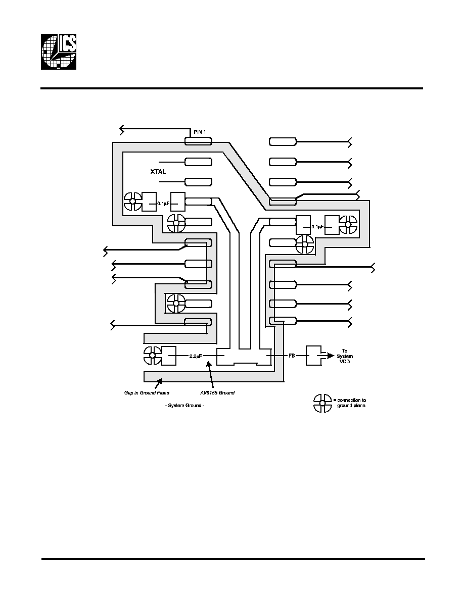
AV9155 Recommended Board Layout
This is the recommended layout for the AV9155 to maximize clock performance. Shown are the power and ground connections,
the ground plane, and the input/output traces.
Use of the isolated ground plane and power connection, as shown, will prevent stray high frequency ground and system noise
from propagating through the device. When compared to using the system ground and power planes, this technique will
minimize output clock jitter. The isolated ground plane should be connected to the system ground plane at one point, near the
2.2�F decoupling cap. For lowest jitter performance, this isolated ground plane should be kept away from clock output pins and
traces. Keeping the isolated ground plane area as small as possible will minimize EMI radiation. Use a sufficient gap between the
isolated ground plane and system ground plane to prevent AC coupling. The ferrite bead in the VDD line optional, but will help
reduce EMI.
The traces to distribute the output clocks should be over a system ground or power supply plane. The trace width should be
about two times the thickness of the PC board between the trace and the underlying plane. These guidelines help minimize clock
jitter and EMI radiation. The traces to distribute power should be as wide as possible.
10
AV9155
Ordering Information
Example:
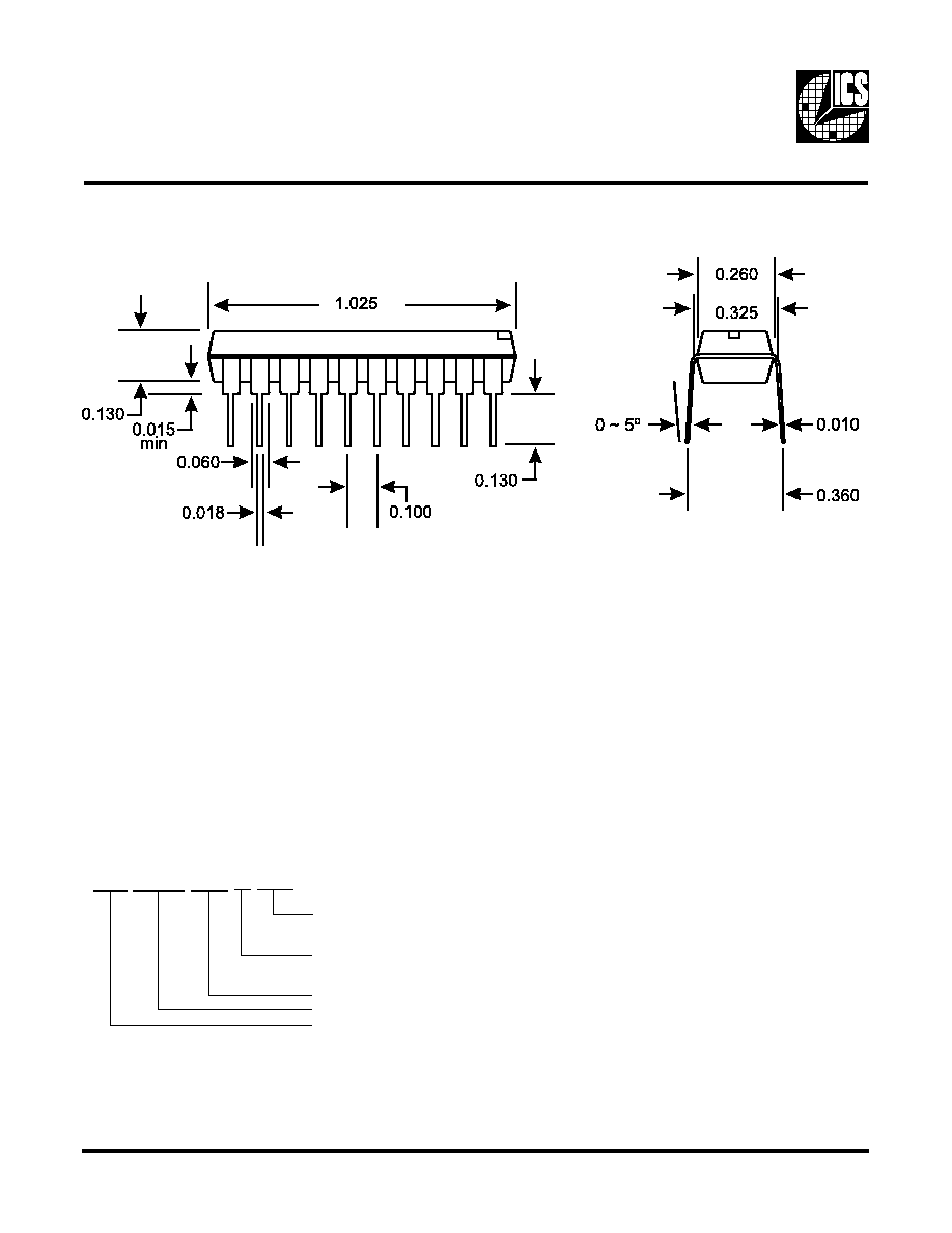
20-Pin DIP Package
AV9155-01N20, AV9155-02N20,
AV9155-23N20, AV9155-36N20
Notes:
Tape and reel packaging should be ordered with the suffix T&R. For instance, if the -01 in DIP and tape & reel is required, order
the part as AV9155-01CN20T&R.
ICS XXXX-PPP M X#W
Lead Count & Package Width
Lead Count=1, 2 or 3 digits
W=.3 SOIC or .6 DIP; None=Standard Width
Package Type
N=DIP (Plastic#)
T&R=Tape and Reel
Pattern Number (2 or 3 digit number for parts with ROM code patterns)
Device Type (consists of 3 or 4 digit numbers)
Prefix
ICS, AV=Standard Device

11
AV9155
Ordering Information
AV9155-01W20, AV9155-02M20,
AV9155-23M20, AV9155-36M20
LEAD COUNT
14L
16L
18L
20L
24L
28L
32L
DIMENSION L
0.354
0.404
0.454
0.504
0.604
0.704
0.804
ICS XXXX-PPP M X#W
Lead Count & Package Width
Lead Count=1, 2 or 3 digits
W=.3 SOIC or .6 DIP; None=Standard Width
Package Type
W=SOIC
T&R=Tape and Reel
Pattern Number (2 or 3 digit number for parts with ROM code patterns)
Device Type (consists of 3 or 4 digit numbers)
Prefix
ICS, AV=Standard Device
Example: