ICS1493-17
MDS 1493-17 A
1
Revision 101005
I n t e gra t e d C i r c u i t S y s t e m s
5 2 5 R a c e S t r e e t , S a n J o s e, C A 9 5 1 2 6
t e l ( 4 0 8 ) 2 9 7 - 1 2 0 1
w w w. i c s t . c o m
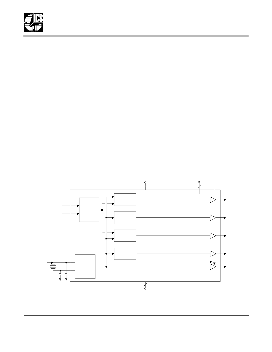
Clock Synthesizer for Portable Systems
P R E L I M I N A R Y I N F O R M A T I O N
Description
The ICS1493-17 is a low-power, low-jitter clock
synthesizer designed to replace multiple crystals and
oscillators in portable audio/video systems. The device
generates a 37 MHz processor clock, a 48 MHz USB
clock, a fixed 22.5792 MHz audio clock, a selectable
24.576 MHz or 22.5792 MHz audio clock, and a 27MHz
reference clock for video. Using ICS' proprietary mix of
analog and digital Phase-Locked Loop (PLL)
technology, the device spreads the frequency spectrum
of the 37 MHz output, reducing the peak amplitude of
by up to 16 dB. An output enable (OE) pin lowers the
chip power consumption while tri-stating all outputs.
Features
�
Extremely low operating current (11 mA)
�
Packaged in 20-pin QFN (Pb-free)
�
Input crystal or clock frequency of 27 MHz
�
Output reference frequency of 27 MHz
�
Fixed output frequencies of 37 MHz, 48 MHz and
22.5792 MHz
�
Selectable output frequency of either 22.5792 MHz
or 24.576 MHz
�
Configurable spread spectrum on 37 MHz output
�
Operating core voltage of 1.8 V
�
Output voltage of 1.8 V or 2.5 V
�
Advanced, low-power CMOS process
Block Diagram
X1
X2
PLL1
(Spread)
PLL2
Crystal
Oscillator/
Clock
Buffer
27 MHz
clock or
crystal input
Optional tuning
capacitors
VDD
GND
27M
37M
3
5
PLL3
22/24M
PLL4
22M
SCK
48M
IIC
Control
Logic
SDATA
OE
VDDO
2
Clock Synthesizer for Portable Systems
MDS 1493-17 A
2
Revision 101005
I n t e gr a t e d C i r c u i t S y s t e m s
5 2 5 R a c e S t r e e t , S a n J o s e, C A 9 5 1 2 6
t e l ( 4 0 8 ) 2 9 7 - 1 2 0 1
w w w. i c s t . c o m
ICS1493-17
P R E L I M I N A R Y I N F O R M A T I O N
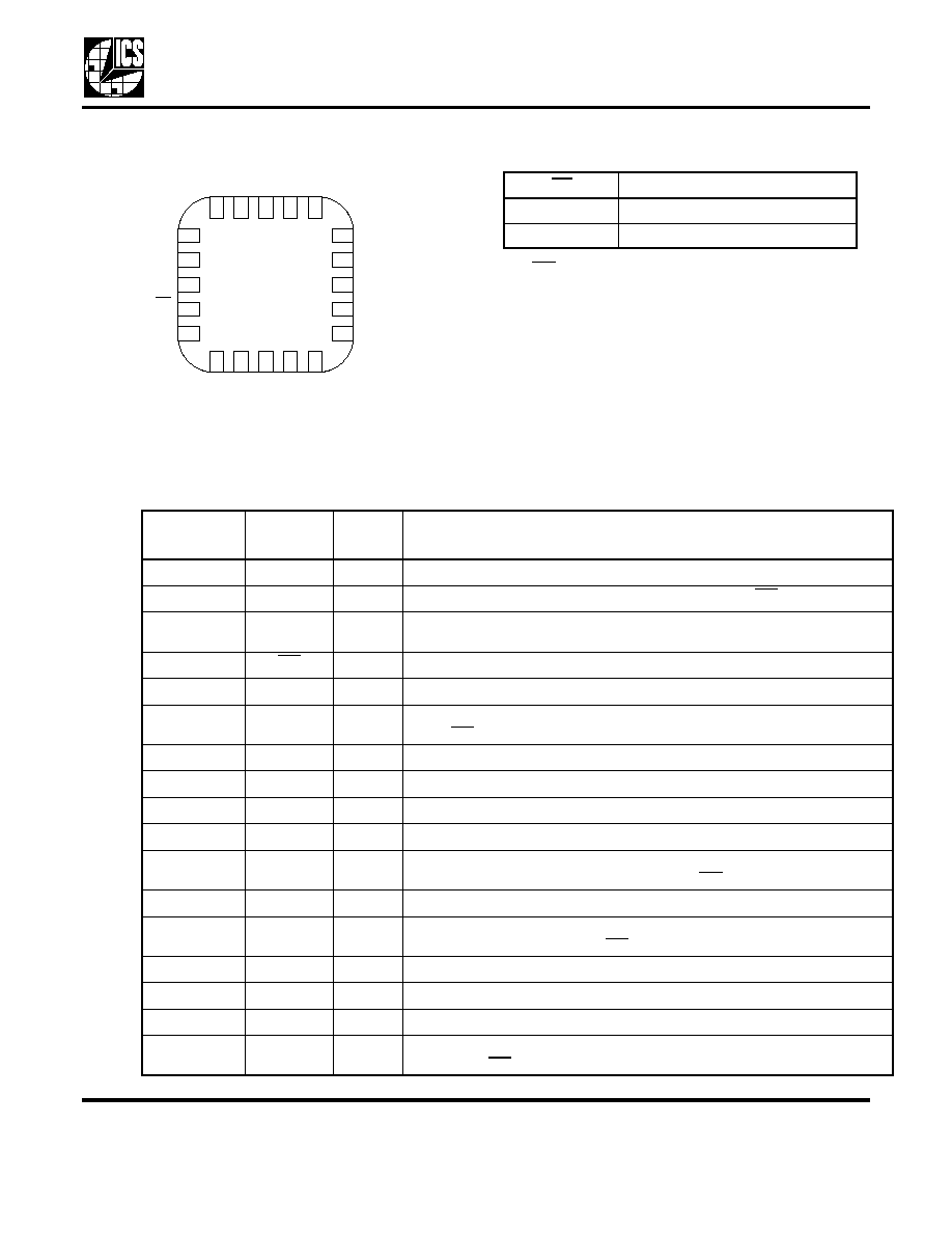
Pin Assignment
Output Enable Table
Note: OE pin has an internal pull-down resistor.
Pin Descriptions
1
GND
20-pin QFN
48M
VDDO
OE
VDD
GND
VDD
37M
VDDO
22/24M
X1
X2
VD
D
27M
GN
D
22M
GN
D
SC
K
SD
A
T
A
GN
D
6
11
16
OE
Clock Output State
0
Normal Operation
1
Hi-Z
Pin
Number
Pin
Name
Pin
Type
Pin Description
1
GND
Power
Connect to ground.
2
48M
Output
48 MHz clock output. High impedance state when OE=1.
3
VDDO
Power
Output voltage level. Connect to +1.8 or 2.5 V. Same voltage as pin
12.
4
OE
Input
Output Enable pin. See table above. Internal pull-down resistor.
5
VDD
Power
Connect to +1.8 V.
6
22M
Output
22.5792 MHz clock output. Internal pull-down. High impedance state
when OE=1.
7
GND
Power
Connect to ground.
8
SCK
Input
I
2
C bus clock pin. Internal pull-up resistor.
9
SDATA
Input
I
2
C bus data pin. Internal pull-up resistor.
10
GND
Power
Connect to ground.
11
22/24M
Output
Selectable output clock of either 22.5792M or 24.576M. See table.
Internal pull-down. High impedance state. OE=1.
12
VDDO
Power
Output voltage level. Connect to +1.8 or 2.5 V. Same voltage as pin 3.
13
37M
Output
Spread spectrum 37 MHz clock output. See table. Internal pull-down.
High impedance state when OE=1.
14
VDD
Power
Connect to +1.8 V.
15
GND
Power
Connect to ground.
16
GND
Power
Connect to ground.
17
27M
Output
27 MHz reference clock output. Internal pull-down. High impedance
state when OE=1.

Clock Synthesizer for Portable Systems
MDS 1493-17 A
3
Revision 101005
I n t e gr a t e d C i r c u i t S y s t e m s
5 2 5 R a c e S t r e e t , S a n J o s e, C A 9 5 1 2 6
t e l ( 4 0 8 ) 2 9 7 - 1 2 0 1
w w w. i c s t . c o m
ICS1493-17
P R E L I M I N A R Y I N F O R M A T I O N
.
External Components
Decoupling Capacitor
As with any high-performance mixed-signal IC, the
ICS1493-17 must be isolated from system power
supply noise to perform optimally.
A decoupling capacitor of 0.01�F must be connected
between each VDD and the PCB ground plane.
Series Termination Resistor
Clock output traces over one inch should use series
termination. To series terminate a 50
trace (a
commonly used trace impedance), place a 33
resistor
in series with the clock line, as close to the clock output
pin as possible. The nominal impedance of the clock
output is 20
.
I
2
C External Resistor Connection
The SCK and SDATA pins can be connected to any
voltage between 1.71 V and 2.625 V.
Crystal Load Capacitors
No external crystal load capacitors are required. To
save discrete component cost, the ICS1493-17
integrates on-chip capacitance to support a crystal with
CL=10 pF. It is important to keep stray capacitance to a
minimum by using very short PCB traces (and no vias)
between the crystal and device.
PCB Layout Recommendations
For optimum device performance and lowest output
phase noise, the following guidelines should be
observed.
1) The 0.01�F decoupling capacitors should be
mounted on the component side of the board as close
to the VDD pin as possible. No vias should be used
between the decoupling capacitors and VDD pins. The
PCB trace to VDD pins should be kept as short as
possible, as should the PCB trace to the ground via.
2) The external crystal should be mounted just next to
the device with short traces. The X1 and X2 traces
should not be routed next to each other with minimum
spaces, instead they should be separated and away
from other traces.
3) To minimize EMI, the 33
series termination resistor
should be placed close to the clock output.
4) An optimum layout is one with all components on the
same side of the board, minimizing vias through other
signal layers. Other signal traces should be routed
away from the ICS1493-17. This includes signal traces
just underneath the device, or on layers adjacent to the
ground plane layer used by the device.
18
VDD
Power
Connect to +1.8 V.
19
X2
Output
Connect to 27 MHz crystal or float for clock input.
20
X1
Input
Crystal connection. Connect to 27 MHz crystal or clock input.
Pin
Number
Pin
Name
Pin
Type
Pin Description
Clock Synthesizer for Portable Systems
MDS 1493-17 A
4
Revision 101005
I n t e gr a t e d C i r c u i t S y s t e m s
5 2 5 R a c e S t r e e t , S a n J o s e, C A 9 5 1 2 6
t e l ( 4 0 8 ) 2 9 7 - 1 2 0 1
w w w. i c s t . c o m
ICS1493-17
P R E L I M I N A R Y I N F O R M A T I O N
Absolute Maximum Ratings
Stresses above the ratings listed below can cause permanent damage to the ICS1493-17. These ratings,
which are standard values for ICS commercially rated parts, are stress ratings only. Functional operation of
the device at these or any other conditions above those indicated in the operational sections of the
specifications is not implied. Exposure to absolute maximum rating conditions for extended periods can
affect product reliability. Electrical parameters are guaranteed only over the recommended operating
temperature range.
Recommended Operation Conditions
DC Electrical Characteristics
Unless stated otherwise, VDD = 1.8 V -0.1 V/+0.2 V, VDDO=2.5 V �5%, Ambient Temp -10
�C to +80�C
Item
Rating
Supply Voltage, VDD
-0.5 V to 5 V
All Inputs
-0.5 V to VDD+0.5 V
All Outputs
-0.5 V to 2.5V+0.5 V
Storage Temperature
-65 to +150
�C
Junction Temperature
125
�C
Soldering Temperature
260
�C
ESD (HBM)
2000V min.
MSL (Moisture Sensitivity Level)
3
Parameter
Min.
Typ.
Max.
Units
Ambient Operating Temperature
-10
+80
�C
Power Supply Voltage (measured in respect to GND)
+1.70
+2.00
V
Output Power Supply Voltage (with respect to GND)
+1.71
+2.625
V
Parameter
Symbol
Conditions
Min.
Typ.
Max.
Units
Operating Voltage
VDD
1.7
2.0
V
Supply Current
IDD
No load,VDDO=2.5 V
13
16
mA
No load,VDDO=1.8 V
11
15
mA
Input High Voltage
V
IH
0.7VDD
V
Input Low Voltage
V
IL
0.3VDD
V
Output High Voltage
V
OH
I
OH
= -2 mA
0.8VDDO
V
Output Low Voltage
V
OL
I
OL
= +2 mA
0.2VDDO
V
Input Capacitance, inputs
C
IN
5
pF
Load Capacitance, X1 and X2
C
L
No internal load
capacitance
5
pF
Clock Synthesizer for Portable Systems
MDS 1493-17 A
5
Revision 101005
I n t e gr a t e d C i r c u i t S y s t e m s
5 2 5 R a c e S t r e e t , S a n J o s e, C A 9 5 1 2 6
t e l ( 4 0 8 ) 2 9 7 - 1 2 0 1
w w w. i c s t . c o m
ICS1493-17
P R E L I M I N A R Y I N F O R M A T I O N
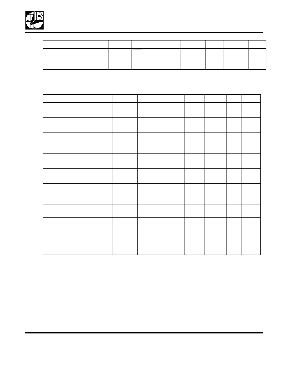
AC Electrical Characteristics
Unless stated otherwise, VDDO = 2.5 V �5%, Ambient Temperature -10
�C to +80�C
Note 1: Measured with a 5 pF load.
Note 2: Finish from prior cycle to start of new cycle.
Internal Pull-down Resistor
R
PD
OE, 48M, 22M,
22/24M, 37M, 27M
75
250
k
Internal Pull-up Resistor
R
Pu
SCK, SDATA
100
500
k
Parameter
Symbol
Conditions
Min.
Typ.
Max.
Units
Input Frequency
f
IN
27
MHz
Output Rise Time
t
OR
20% to 80%, Note 1
0.7
1.5
2.2
ns
Output Fall Time
t
OF
80% to 20%, Note 1
0.7
1.5
2.2
ns
Output Impedance
R
O
VO=VDDO/2
33
46
68
Output Clock Duty Cycle
VDDO/2, 27 MHz,
Note 1
40
50
60
%
VDDO/2, Note 1
45
50
55
%
Frequency Synthesis Error
All outputs
0
ppm
Modulation Rate
30
35
40
kHz
Short Term Jitter
Cycle-to-Cycle
150
300
ps
Long Term Jitter
27 MHz, n=1000
600
ps
Long Term Jitter
48 MHz, n=1000
800
ps
Long Term Jitter
22M and 22/24M,
n=1000
1.2
ns
Long Term Jitter
37 MHz non-spread,
n=1000
1.5
6
ns
Power-up Time
t
PU
From minimum VDD
to outputs stable
1.5
3
ms
Output Enable Time
50
ns
Output Disable Time
20
ns
Switching Time
22/24M, Note 2
100
ns
Parameter
Symbol
Conditions
Min.
Typ.
Max.
Units
Clock Synthesizer for Portable Systems
MDS 1493-17 A
6
Revision 101005
I n t e gr a t e d C i r c u i t S y s t e m s
5 2 5 R a c e S t r e e t , S a n J o s e, C A 9 5 1 2 6
t e l ( 4 0 8 ) 2 9 7 - 1 2 0 1
w w w. i c s t . c o m
ICS1493-17
P R E L I M I N A R Y I N F O R M A T I O N
AC Electrical Characteristics
Unless stated otherwise, VDDO = 1.8 V �0.1 V, Ambient Temperature -10
�C to +80�C
Note 1: Measured with a 5 pF load.
Note 2: Finish from prior cycle to start of new cycle.
Parameter
Symbol
Conditions
Min.
Typ.
Max.
Units
Input Frequency
f
IN
27
MHz
Output Rise Time
t
OR
20% to 80%, Note 1
1.1
2.2
3.3
ns
Output Fall Time
t
OF
80% to 20%, Note 1
1.1
2.2
3.3
ns
Output Impedance
R
O
VO=VDDO/2
33
46
68
Output Clock Duty Cycle
VDDO/2, 27 MHz,
Note 1
40
50
60
%
VDDO/2, Note 1
45
50
55
%
Absolute Clock Period Jitter
Note 1
� 225
ps
Frequency Synthesis Error
All outputs
0
ppm
Modulation Rate
30
35
40
kHz
Short Term Jitter
Cycle-to-cycle
225
375
ps
Long Term Jitter
27 MHz, n=1000
900
ps
Long Term Jitter
48 MHz, n=1000
750
ps
Long Term Jitter
22M and 22/24M,
n=1000
1200
ps
Long Term Jitter
37 MHz, n=1000
2.5
9
ns
Power-up Time
t
PU
From minimum VDD
to outputs stable
1.5
4
ms
Output Enable Time
50
ns
Output Disable Time
20
ns
Switching Time
22/24M, Note 2
250
ns

Clock Synthesizer for Portable Systems
MDS 1493-17 A
7
Revision 101005
I n t e gr a t e d C i r c u i t S y s t e m s
5 2 5 R a c e S t r e e t , S a n J o s e, C A 9 5 1 2 6
t e l ( 4 0 8 ) 2 9 7 - 1 2 0 1
w w w. i c s t . c o m
ICS1493-17
P R E L I M I N A R Y I N F O R M A T I O N
Serial Data Interface
Data Protocol
The clock driver serial protocol accepts byte write, byte read, block write, and block read operations from the
controller. For block write/read operation, the bytes must be accessed in sequential order from lowest to highest
byte (most significant bit first) with the ability to stop after any complete byte has been transferred. For byte write
and byte read operations, the system controller can access individually indexed bytes. The offset of the indexed
byte is encoded in the command code, as described in the following table.
The block write and block read protocol is outlined in the table below, followed by the corresponding byte write and
byte read protocol. The slave receiver address is 11010010 (D2h).
Bit
Description
7
0 = Block read or block write operation, 1 = Byte read or byte write operation
(6:0)
Byte offset for byte read or byte write operation. For block read or block write operations,
these bits should be '0000000'.
Block Write Protocol
Block Read Protocol
Bit
Description
Bit
Description
1
Start
1
Start
2:8
Slave address - 7 bits
2:8
Slave address - 7 bits
9
Write = 0
9
Write = 0
10
Acknowledge from slave
10
Acknowledge from slave
11:18
Command code -- 8 bit
`00000000' stands for block operation
11:18
Command code - 8 bit
`00000000' stands for block operation
19
Acknowledge from slave
19
Acknowledge from slave
20:27
Byte count -- 8 bits
20
Repeat start
28
Acknowledge from slave
21:27
Slave address -- 7 bits
29:36
Data byte 0 -- 8 bits
28
Read = 1
37
Acknowledge from slave
29
Acknowledge from slave
38:45
Data byte 1 -- 8 bits
30:37
Byte count from slave -- 8 bits
46
Acknowledge from slave
38
Acknowledge from master
....
.............................
39:46
Data byte from slave -- 8 bits
....
Data byte (N-1) -- 8 bits
47
Acknowledge from master
....
Acknowledge from slave
48:55
Data byte from slave -- 8 bits
....
Data byte N -- 8 bits
56
Acknowledge from master
....
Acknowledge from slave
....
Data byte N from slave -- 8 bits
....
Stop
....
Not Acknowledge from master
....
Stop

Clock Synthesizer for Portable Systems
MDS 1493-17 A
8
Revision 101005
I n t e gr a t e d C i r c u i t S y s t e m s
5 2 5 R a c e S t r e e t , S a n J o s e, C A 9 5 1 2 6
t e l ( 4 0 8 ) 2 9 7 - 1 2 0 1
w w w. i c s t . c o m
ICS1493-17
P R E L I M I N A R Y I N F O R M A T I O N
.
Byte 0: Vendor ID, Revision Code
Byte Write Protocol
Byte Read Protocol
Bit
Description
Bit
Description
1
Start
1
Start
2:8
Slave address - 7 bits
2:8
Slave address - 7 bits
9
Write = 0
9
Write = 0
10
Acknowledge from slave
10
Acknowledge from slave
11:18
Command code -- 8 bit
`10000000' stands for byte operation,
bits[1:0] of the command code represents
the offset of the byte to be accessed
11:18
Command code -- 8 bit
`10000000' stands for byte operation, bits[1:0]
of the command code represents the offset of
the byte to be accessed
19
Acknowledge from slave
19
Acknowledge from slave
20:27
Data byte from master-- 8 bits
20
Repeat start
28
Acknowledge from slave
21:27
Slave address -- 7 bits
29
Stop
28
Read = 1
29
Acknowledge from slave
30:37
Data byte from slave -- 8 bits
38
Not Acknowledge from master
39
Stop
Bit
@Pup
Name
Description
7
0
Revision Code(MSB)
Revision Code
6
0
Revision Code
Revision Code
5
0
Revision Code
Revision Code
4
1
Revision Code(LSB)
Revision Code
3
1
Vendor ID(MSB)
Vendor ID
2
1
Vendor ID
Vendor ID
1
1
Vendor ID
Vendor ID
0
1
Vendor ID(LSB)
Vendor ID

Clock Synthesizer for Portable Systems
MDS 1493-17 A
9
Revision 101005
I n t e gr a t e d C i r c u i t S y s t e m s
5 2 5 R a c e S t r e e t , S a n J o s e, C A 9 5 1 2 6
t e l ( 4 0 8 ) 2 9 7 - 1 2 0 1
w w w. i c s t . c o m
ICS1493-17
P R E L I M I N A R Y I N F O R M A T I O N
Byte 1: Control Register
Byte 2: Control Register
Bit
@Pup
Name
Description
7
1
REF
REF Output Enable
0 = Disable, Output pulled low, 1 = Enable
6
1
37SS
37SS Output Enable
0 = Disable, Output pulled low, corresponding PLL shut off.
1 = Enable
5
1
48M
48M Output Enable
0 = Disable, Output pulled low, 1 = Enable
4
1
22/24M
22/24M Clock Output Enable
0 = Disable, Output pulled low, 1 = Enable
3
0
22M
22M Output Enable
0 = Disable, Output pulled low and corresponding PLL off,
1 = Enable
2
1
Reserved
Reserved
1
1
Reserved
Reserved
0
1
22/24M SEL
22/24M Clock Select
1 = 24.576 MHz, 0 = 22.5792 MHz
Bit
@Pup
Name
Description
7
0
Reserved
Reserved
6
0
Reserved
Reserved
5
0
Reserved
Reserved
4
0
Reserved
Reserved
3
0
Reserved
Reserved
2
0
SS Table
Bit 2:0=000: No Spread
Bit 2:0=001: -0.5% Spread
Bit 2:0=010:-1.0% Spread
Bit 2:0=011: No Spread
Bit 2:0=100: -2.0% Spread
Bit 2:0=101: No Spread
Bit 2:0=110: -3.0% Spread
Bit 2:0=111: No Spread
1
1
SS Table
0
0
SS Table

Clock Synthesizer for Portable Systems
MDS 1493-17 A
10
Revision 101005
I n t e gr a t e d C i r c u i t S y s t e m s
5 2 5 R a c e S t r e e t , S a n J o s e, C A 9 5 1 2 6
t e l ( 4 0 8 ) 2 9 7 - 1 2 0 1
w w w. i c s t . c o m
ICS1493-17
P R E L I M I N A R Y I N F O R M A T I O N
Thermal Characteristics
Marking Diagram
Notes:
1. ###### is the lot code.
2. YYWW is the last two digits of the year and the week number that the part was assembled.
3. "L" denotes Pb (lead) free package.
4. Bottom marking: (origin). Origin = country of origin if not USA.
Parameter
Symbol
Conditions
Min.
Typ.
Max.
Units
Thermal Resistance Junction to
Ambient
JA
Still air
39
�C/W
JA
1 m/s air flow
36
�C/W
JA
2.5 m/s air flow
34
�C/W
1
6
11
16
93K17L
######
YYWW
Clock Synthesizer for Portable Systems
MDS 1493-17 A
11
Revision 101005
I n t e gr a t e d C i r c u i t S y s t e m s
5 2 5 R a c e S t r e e t , S a n J o s e, C A 9 5 1 2 6
t e l ( 4 0 8 ) 2 9 7 - 1 2 0 1
w w w. i c s t . c o m
ICS1493-17
P R E L I M I N A R Y I N F O R M A T I O N
Package Outline and Package Dimensions
(20-pin QFN)
Package dimensions are kept current with JEDEC Publication No. 95
Ordering Information
Parts that are ordered with a "LF" suffix to the part number are the Pb-Free configuration and are RoHS compliant.
While the information presented herein has been checked for both accuracy and reliability, Integrated Circuit Systems (ICS)
assumes no responsibility for either its use or for the infringement of any patents or other rights of third parties, which would
result from its use. No other circuits, patents, or licenses are implied. This product is intended for use in normal commercial
applications. Any other applications such as those requiring extended temperature range, high reliability, or other extraordinary
environmental requirements are not recommended without additional processing by ICS. ICS reserves the right to change any
circuitry or specifications without notice. ICS does not authorize or warrant any ICS product for use in life support devices or
critical medical instruments.
Millimeters
Symbol
Min
Max
A
0.80
1.00
A1
0
0.05
A3
0.20 Reference
b
0.18
0.30
e
0.50 BASIC
N
20
N
D
5
N
E
5
D x E BASIC
4.00 x 4.00
D2
1.95
2.25
E2
1.95
2.25
L
0.45
0.75
Part / Order Number
Marking
Shipping Packaging
Package
Temperature
ICS1493K-17LF
see page 10
Tubes
20-pin QFN
-10 to +80
�C
ICS1493K-17LFT
Tape and Reel
20-pin QFN
-10 to +80
�C
Anvil
Singulation
-- or --
Sawn
Singulation
1
2
N
E
D
Index Area
Top View
Seating Plane
A3
A1
C
A
L
E2
E2
2
D2
D2
2
e
C
0.08
(Ref)
N
D
& N
E
Odd
(Ref)
N
D
& N
E
Even
(N
D
-1)x
(Ref)
e
N
1
2
b
Thermal Base
(Typ)
If N
D
& N
E
are Even
(N
E
-1)x
(Ref)
e
e
2