 | –≠–ª–µ–∫—Ç—Ä–æ–Ω–Ω—ã–π –∫–æ–º–ø–æ–Ω–µ–Ω—Ç: ICS1522M | –°–∫–∞—á–∞—Ç—å:  PDF PDF  ZIP ZIP |
Integrated
Circuit
Systems, Inc.
General Description
Features
∑
Serial programming: Feedback and reference divisors,
VCO gain, phase comparator gain, relative phase and
test modes.
∑
Supports high-resolution graphics - Differential CLK
out-puts to 230 MHz
∑
Eliminates need for multiple ECL output voltage control-
led crystal oscillators and external components
∑
Fully-programmable synthesizer capability - not just a
clock multiplier
∑
Line-locked clock generation capability;
15 - 100 kHz
∑
External feedback loop capability allows graphics
system to be used as the feedback divisor with
synchronous switchover to internal feedback
∑
Small footprint 24-pin SOIC
∑
Coarse and fine phase adjustment permits precise
clocking in video recovery application
Applications
∑
LCD Projector Systems
∑
Multimedia video line locking
∑
Genlock applications
1522RevF050697P
User-Programmable
Video Clock Generator/ Line-Locked
Clock Regenerator
ICS1522
The ICS1522 is a very high performance monolithic phase-
locked loop (PLL) frequency synthesizer. Utilizing ICS's
advanced CMOS mixed-mode technology, the ICS1522
provides a low-cost solution for high-end video clock
generation where synchronization to an external video
source is required.
The ICS1522 has differential video clock outputs (CLK+
and CLK-) that are compatible with industry standard
video DAC.
Operating frequencies are fully programmable with direct
control provided for reference divider, feedback divider
and postscaler.
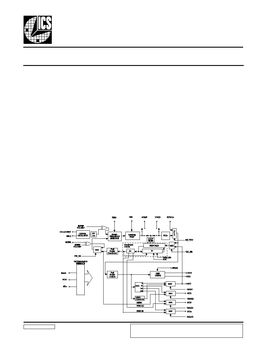
Block Diagram
ICS reserves the right to make changes in the device data identified in this publication
without further notice. ICS advises its customers to obtain the latest version of all
device data to verify that any information being relied upon by the customer is current
and accurate.

2
ICS1522
Overview
The ICS1522 is ideally suited to provide the graphics
system clock signals required by high-performance video
DACs. Fully programmable feedback and reference divider
capability allow virtually any frequency to be generated,
not just simple multiples of the reference frequency. The
ICS1522 uses the latest generation of frequency synthesis
techniques developed by ICS and is completely suitable
for the most demanding video applications.
PLL Synthesizer Description -
Ratiometric Mode
The ICS1522 generates its output frequencies using phase-
locked loop techniques. The phase-locked loop (or PLL) is
a closed-loop feedback system that drives the output
frequency to be ratiometrically related to the reference
frequency pro-vided to the PLL (see Block Diagram). The
reference frequency is generated by an on-chip crystal
oscillator or the reference frequency may be applied to the
ICS1522 from an external frequency source, typically
horizontal sync from another dis-play system.
The phase-frequency detector shown in the Block Diagram
drives the voltage-controlled oscillator, or VCO, to a
frequency that will cause the two inputs to the phase-
frequency detector to be matched in frequency and phase.
This occurs when:
F(VCO): = F(XTAL1) . Feedback Divider
Reference Divider
This expression is exact; that is, the accuracy of the output
frequency depends solely on the reference frequency
provided to the part (assuming correctly programmed
dividers).
The VCO gain is programmable, which permits the ICS1522
to be optimized for best performance at all operating fre-
quencies.
The feedback divider may be programmed for any modulus
from 64 to 2048 in steps of one followed by a divide by 1,
2, 4 or 8 feedback post-scaler.
The reference divider may be programmed for any modulus
from 1 to 1024 in steps of one.
Output Post-scaler
A programmable post-scaler may be inserted between the
VCO and the CLK+ and CLK- outputs of the ICS1522. This
is useful in generating of lower frequencies, as the VCO
has been optimized for high-frequency operation.
The post-scaler allows the selection of dividing the VCO
frequency by either 1, 2, 4 or 8.
Load Clock Divider
The ICS1522 has an additional programmable divider
(referred to in the Block Diagram as the load counter) that
is used to generate the LOAD clock frequency for the
video DAC. The modulus of this divider may be set to 3, 4,
5, 6, 8, or 10 under register control. The design of this
divider permits the output duty factor to be 50/50, even
when odd modulus is selected. The input frequency to this
divider is the output of the output post-scaler described
above.
Digital Inputs - ICS1522
The programming of the ICS1522 is performed serially by
using the SDATA, SCLK, and SELn pins to load the 7, 11
bit internal memory locations.
Single bit changes are accomplished by addressing the
appro-priate memory location and writing only 11 bits of
data, not by writing all 77 data bits.
For proper programming of the ICS1522, it is important
that all transitions of the SELn input occur during the same
state of the SCLK input.
SDATA is shifted into a 15 bit serial register on the rising
edge of SCLK while SELn is low. The first bit loaded is R/
Wn followed by a 3 bit address and 11 bit data (both
address & data are LSB first). When a rising edge of SCLK
occurs while SELn is high (SDATA ignored), the contents
of the serial register are loaded into the addressed 11 bit
memory location if R/Wn is low. If R/Wn is high upon the
above condition, the data from the addressed memory
location is loaded into the serial shift register and SDATA
is set as an output. The 3 bit address and 11 bit data will be
serially shifted out of the ICS1522 on the SDATA pin on
the rising edge of SCLK while SELn is low (see Timing
Diagram).
An additional control pin on the ICS1522, PDEN can be
used to disable the phase-frequency detector in line-locked
applica-tions. When disabled, the phase detector will ignore
any inputs and allow the VCO to coast. This feature is
useful in systems using composite sync.

3
ICS1522
Output Description
The differential output drivers, CLK+ and CLK-, are
current-mode and are designed to drive resistive terminations
in a complementary fashion. The outputs are current-
sinking only, with the amount of sink current programmable
via the IPRG pin. The sink current, which is steered to
either CLK+ or CLK-, is four times the current supplied to
the IPRG pin. For most applications, a resistor from VDDO
to IPRG will set the current to the necessary precision.
Reference Oscillator and
Crystal Selection
The ICS1522 has circuitry on-board to implement a Pierce
oscillator with the addition of a quartz crystal and two
external loading capacitors (EXTREF bit must be set to
logic 0). Pierce oscillators operate the crystal in anti- (also
called parallel-) resonant mode.
Series-resonant crystals may also be used with the ICS1522.
Be aware that the oscillation frequency will be slightly
higher than the frequency that is stamped on the can
(typically 0.025-0.05%).
As the entire operation of the phase-locked loop depends
on having a stable reference frequency, we recommend
that the crystal be mounted as closely as possible to the
package. Avoid routing digital signals or the ICS1522
outputs underneath or near these traces. It is also desirable
to ground the crystal can to the ground plane, if possible.
If an external reference frequency source is to be used with
the ICS1522, it is important that it be jitter-free. The rising
and falling edges of that signal should be fast and free of
noise for best results. The loop phase is locked to the rising
edge of the XTAL1/EXTREF input signal, if REF_POL is
set to logic 0. Additionally, the EXTREF bit should be set
to logic 1 to switch in a TTL-compatible buffer at this
input.
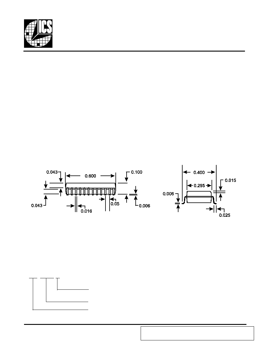
24-Pin SOIC
Line-Locked Operation
Some video applications require a clock to be generated
that is a multiple of horizontal sync. The ICS1522
supports this mode of operation. The reference divider
should be set to divide by one and the desired polarity
(rising or falling) of lock edge should be selected. By
using the phase detector hardware disable mode (PDEN),
the PLL can be made to free-run at the beginning of the
vertical interval of the external video, and can be
reactivated at its completion.
External Feedback Operation
The ICS1522 option also supports the inclusion of an
external counter as the feedback divider of the PLL.
This mode is useful in graphic systems that must be
"genlocked" to external video sources.
When the FBK_SEL bit is set to logic 0, the phase-
frequency detector will use the EXTFBK pin as its
feedback input. The loop phase will be locked to the
rising edges of the signal applied to the EXTFBK input
if FBK_POL is set to logic 0 Synchronous switchover
to the internal feedback can be ac-complished by
setting the FBK-SEL bit to logic 1 while an active
feedback source exists on the EXTFBK pin.
Fine Phase Adjustment
The ICS1522 has the capability of adjusting the pixel
clock phase relative to the input reference phase.
Entire pixels can be added or removed under register
control with sub-pixel adjust-ment accomplished by a
control voltage on the FINE input pin. By utilizing the
fine phase adjust, after first synchronously switching
from external feedback to internal feedback, the graphics
system phase can be precisely controlled relative to
the input horizontal sync.

4
ICS1522
Power-On Initialization
The ICS1522 has an internal power-on reset circuit that
sets the frequency of the CLK+and CLK- outputs to be half
the crystal or reference frequency assuming that they are
between 10 MHz and 25 MHz (refer to default settings in
Register Definition). Because the power-on reset circuit is
on the VDD supply, and because that supply is filtered,
care must be taken to allow the reset to de-assert before
programming. A safe guideline is to allow 20 microseconds
after the VDD supply reaches four volts.
Board Test Support
It is often desirable to statically control the levels of the
output pins for circuit board test. The ICS1522 supports
this through a register programmable mode, AUXEN. When
this mode is set, AUXCLK will directly control the logic
levels of the CLK+ and CLK- pins while OMUX1, OMUX2,
OMUX3, and OMUX4 will control OUT1, OUT2, OUT3
and OUT4, respectively.
Power Supplies and Decoupling
The ICS1522 has three VSS pins to reduce the effects of
package inductance. Both pins are connected to the same
potential on the die (the ground bus). These pins should
connect to the ground plane of the video board as close to
the package as is possible.
The ICS1522 has a VDDO pin which is the supply of +5
volt power to all output drivers. This pin should be connected
to the power plane (or bus) using standard high-frequency
decoupling practice. That is, capacitors should have low
series inductance and be mounted close to the ICS1522.
The VDD pin is the power supply pin for the PLL synthesizer
circuitry and other lower current digital functions. We
recommend that RC decoupling or zener regulation be
provided for this pin (as shown in the recommended
application circuitry). This will allow the PLL to "track"
through power supply fluctuations without visible effects.
PIN NUMBER
PIN NAME
TYPE
DESCRIPTION
1
IPUMP
OUT
Charge Pump output (External loop filter applications)
2
SDATA
IN/OUT
Serial Data Input/Output
3
SCLK
IN
Serial Clock Input
4
SELn
IN
Serial Port enable (active Low)
5
AVDD
PWR
Analog +5 Volt Supply
6
XTAL1/EXTREF
IN
External Reference Input / Xtal Oscillator Input
7
XTAL2
OUT
Xtal Oscillator Output
8
FINE
IN
Fine Phase Adjust Input
9
VSS
PWR
Ground
10
VSS
PWR
Ground
11
OUT4
OUT
Output 4
12
OUT3
OUT
Output 3
13
VDDO
PWR
Output Driver +5 Volt Supply
14
OUT2
OUT
Output 2
15
OUT1
OUT
Output 1
16
VSS
PWR
Ground
17
IPRG
IN
Output Driver Current Programming Input
18
CLK-
OUT
Differential CLK - Output
19
CLK+
OUT
Differential CLK + Output
20
VDD
PWR
Digital +5 Volt Supply
21
PDEN
IN
Phase Detector Enable (Active High)
22
EXTFBK
IN
External Feedback Input
23
EXTVCO
IN
External VCO input
24
VVCO
IN
VCO Control Voltage Input (External loop filter applications)
Pin Discriptions

5
ICS1522
ICS1522 Register Definition
REG#
BIT(S)
BIT REF.
DESCRIPTION
0
0-10
F[0:10]
Feedback Divider (Default=04F, Modulus=80) Divides the VCO
by the set modulus Modulus Range=64 to 2048;
Modulus=Value+1
1
0-7
LO[0:7]
Feedback Sync Pulse LO (Default=03) Feedback Divider output,
but with programmable phase; LO[0:7] <F[3:10].
2
0-7
HI[0:7]
Feedback Sync Pulse HI (Default=06) Feedback Divider output,
but with programmable phase; HI[0:7] <F[3:10].
3
0-9
R[0:9]
Reference Divider (Default=013, Modulus=20) Divides the
XTAL/EXTREF by the set modulus Modulus Range=1 to 1024;
Modulus=Value+1
3
1 0
REF_POL
External Reference Polarity (Default=0) 0=Positive Edge;
1=Negative Edge
4
0-2
VCO[0:2]
VCO Gain (Default=4)
VCO(2)
VCO(1)
VCO(0)
VCO GAIN
0
0
0
10 MHz/V
0
0
1
15 MHz/V
0
1
0
20 MHz/V
0
1
1
25 MHz/V
1
0
0
45 MHz/V
1
0
1
60 MHz/V
1
1
0
75 MHz/V
1
1
1
90 MHz/V
6
ICS1522
REG#
BIT(S)
BIT REF.
DESCRIPTION
4
3-5
PFD (0;2)
Phase Frequency Detector Gain
4
6
PDEN
Phase Frequency Detector Enable
(Default=1) 0=PFD Disable; 1=PFD Enable
4
7
INT_FLT
Loop Filter Select (Default=1)
0=External Loop Filter (IPUMP & VVCO active)
1=Internal Loop Filter
4
8
INT_VCO
VCO Select (Default=1)
0=External VCO (EXTVCO active)
1=Internal VCO
4
9
CLK_SEL
Feedback Divider Clock Input Select (Default=0)
0=VCO; 1=OUT1
4
1 0
RESERVED
Must be set to one.
5
0
FBK_SEL
Feedback Select (Default=1)
0=External Feedback (EXTFBK active)
1=Internal Feedback An active external feedback signal at EXTFBK
is necessary to synchronously switch to internal.
5
1
FBK_POL
External Feedback Polarity (Default=0)
0=Positive Edge; 1=Negative Edge
5
2
ADD
Addition of 1 VCO Cycle (Default=0)
Toggle (0 to 1 to 0) to add 1 VCO cycle.
5
3
SWLW
Removal of 1 VCO Cycle (Default=0)
Toggle (0 to 1 to 0) to remove 1 VCO cycle.
PFD(2)
PFD(1)
PFD(0)
PFD GAIN
FINE PHASE
ADJ.
0
0
0
.2344uA/2
rad
3ns/V
0
0
1
.9375uA/2
rad
3ns/V
0
1
0
3.750uA/2
rad
3ns/V
0
1
1
15.00uA/2
rad
3ns/V
1
0
0
1.875uA/2
rad
6ns/V
1
0
1
7.500uA/2
rad
6ns/V
1
1
0
30.00uA/2
rad
1.5ns/V
1
1
1
120.0uA/2
rad
.375ns/V

7
ICS1522
REG#
BIT(S)
BIT REF.
DESCRIPTION
5
4-5
PDA(0:1)
Output Post-scaler (Default=0)
Input=VCO; Output = Differential Output
5
6-7
PDB(0:1)
Feedback Post-scaler (Default=3)
Input=Feedback Divider; Output=PFD
5
8
LD_LG
Fine Phase Adjust Lead/Lag (Default=1)
1=FBK will lag REF at input to PFD
0=FBK will lead REF at input to PFD
5
9
F_EN
Fine Phase Adjust Enable (Default=))
0=Disable; 1=Enable
5
1 0
RESERVED
Must be set to one.
6
0-2
L(0:2)
Load Counter (Default=7)
PFD(2)
PFD(0)
DIVIDE BY
0
0
8
0
1
4
1
0
2
1
1
1
PDB(1)
PDB(0)
DIVIDE BY
0
0
8
0
1
4
1
0
2
1
1
1
L(2)
L(1)
L(0)
DIVIDE BY
0
0
0
31-pos, 0-neg
0
0
1
4 pos edge
0
1
0
4 neg edge
0
1
1
51-neg, 0-pos
1
0
0
6 pos edge
1
0
1
8 neg edge
1
1
0
8 neg edge
1
1
1
10 neg edge

8
ICS1522
REG#
BIT(S)
BIT REF.
DESCRIPTION
6
3
OMUX1
OUT1 Select (Default=0)
0=Load Counter Output 1=Diff.
Output Divided by 4 at 0 Degrees
OUT1 will track OMUX1 when AUXEN=1
6
4
OMUX2
OUT2 Select (Default=0)
0=Internal Feedback Pulse 1=Diff.
Output Divided by 4 at 90 Degrees
OUT2 will track OMUX2 when AUXEN=1\
6
5
OMUX3
OUT3 Select (Default=0)
0=Feedback Sync Pulse LO
1=Diff. Output Divided by 4 at 180
Degrees OUT3 will track OMUX3 when AUXEN=1
6
6
OMUX4
OUT4 Select (Default=1)
0=Feedback Sync Pulse HI
1=Diff. Output Divided by 4 at 270 Degrees
OUT4 will track OMUX4 when AUXEN=1
6
7
DACRST
Output Reset (Default=0)
When set to one, the CLK+ output is
kept high and the CLK-output is kept low. When returned to zero,
the CLK+ and CLK-outputs will resume toggling on a rising edge
of the OUT1 output (programmed for Load Counter) within +/- 1
clock period.
6
8
AUXEN
Output Test Mode (Default=0)
0=Normal Output Operation
1=Output Test Mode (see OMUX1-4 and AUXCLK)
6
9
AUXCLK
Output Clock when in Test Mode (Default=0)
CLK+ and CLK- will track AUXCLK when AUXEN=1
6
1 0
EXTREF
XTAL/EXTREF Input Buffer (Default=0)
0=Crystal Input Operation
1=External Reference Input Operation
9
ICS1522
Serial Programming Timing Diagram
NOTES:
1. R/Wn, READ=1 and WRITE=0
2. Address and data transmitted least significant bit first
3. 16 Positive-edge clocks required for complete data read/write (1-R/Wn, 3-Address,
11-Data, and 1 load data W/SELn HIGH)
4. SELn's positive and negative transitions must occur on the same state of SCLK
5. An ICS1522 read consists of two consecutive cycles (1st cycle - SDATA is an input,
2nd cycle - SDATA is an output)

10
ICS1522
Absolute Maximum Ratings
VDD, VDDO (measured to VSS) ................. 7.0V
Digital Inputs VSS ....................................... -0.5 to VDD to 0.5V
Digital Outputs VSS ..................................... -0.5 to VDDO to +0.5V
Storage temperature .................................... -65 to 150 ∞ C DC Characteristics
Junction temperature ................................... 175∞ C
Soldering temperature ................................. 260∞C
Recommended Operating Conditions
VDD, VDDO (measured to VSS) ................ 4.75 to 5.25V
Operating Temperature (Ambient) ............ 0 to 70∞C
DC Characteristics
TTL-Compatible Inputs
PDEN, EXTFBK, SDATA, SCLK, SELn, and XTAL1/EXTREF (when EXTREF bit set to 1)
PARAMETER
SYMBOL
CONDITIONS
MIN
MAX
UNITS
Input High Voltage
V
ih
2.0
VDD+0.5
V
Input Low Voltage
V
il
VSS - 0.5
0.8
V
Input Hysteresis
.20
.60
V
Input High Current
I
ih
V
ih
=V
DD
-
10
µA
Input Low Current
I
il
V
il
=0.0
-
200
µA
Input Capacitance
C
in
-
8
pF
EXTVCO Input
PARAMETER
SYMBOL
CONDITIONS
MIN
MAX
UNITS
Input High Voltage
V
x
h
3.75
V
D
D
+5
V
Input Low Voltage
V
x
1
V
S
S
- 0.5
1.25
V
CLK+, CLK - Outputs
PARAMETER
SYMBOL
CONDITIONS
MIN
MAX
UNITS
Differential Output Voltage
0.6
-
V
OUT1, OUT2, OUT3, OUT4 Outputs
PARAMETER
SYMBOL
CONDITIONS
MIN
MAX
UNITS
Output High Voltage
(I
OH
=4.0mA)
2.4
-
V
Output Low Voltage
(I
ol
=8.0mA)
-
0.4
V

11
ICS1522
AC Characteristics
SYMBOL
PARAMETER
MIN
TYP
MAX
UNITS
Fvco
VCO Frequency
14
230
MHz
Fxtal
Crystal Frequency
5
20
MHz
Cpar
Crystal Oscillator Loading Capacitance
20
pF
FHSYNC
Horizontal Sync Rate
15
100
kHz
Txhi
XTAL1 High Time (when driven externally)
8
ns
Txlo
XTAL1 Low Time (when driven externally)
8
ns
TJIT
Phase Jitter (see Note 1)
1
ns
Tlock
PLL Acquire Time (to within 1%)
500
ms
Idd
VDD Supply Current
15
mA
Iddo
VDDO Supply Current
(excluding CLK+/- termination)
20
mA
ANALOG INPUTS
TFINE
Fine Phase Adjustment Range
0
15
ns
VFINE
Control Voltage for FINE
0
VDD/2
VDC
A
FINE Input Bias Current
20
nA
A
Capacitance of FINE Input
100
pf
A
Bandwidth of FINE Input (3dB)
0.5
1.5
kHz
DIGITAL INPUT
A
SELn, SDATA Setup Time
10
ns
A
SELn, SDATA Hold Time
10
ns
A
SCLK Pulse Width (Thi or Tlo)
20
ns
A
SCLK Frequency
20
MHz
A
Phase-frequency detector enable time
50
ns
A
Phase-frequency detector disable time
50
ns
DIGITAL OUTPUTS
TSKEW
Time Skew between CLK+, CLK-
500
ps
FCLK
CLK+ and CLK- Clock Rate
230
MHz
GAINS
VCO
VCO Gain, VCO(0:2)
10
90
MHz/V
PFD
Phase Detector Gain, PFD (0:2)
.23
120
mA/2prad
Note 1: TJIT is the total uncertainty of the phase measured at the start of a video line on a 350 MHz oscilloscope under
these conditions: HSYNC pin driven with crystal oscillator at 48.363 kHz; FVCO = 65.000 MHz; M =0 (divide
by 1 on the output; and N = 1343 (1344 clocks per line).
12
ICS1522
Memory Definition
ICS1522 memory is loaded serially with the least significant bit clocked into the device first. After the R/Wn bit, the next
three bits of the programming word (15 bits) hold the memory location to be loaded. The least significant 11 bits are the
data to be loaded (see Timing Diagram).
MEMORY
ADDRESS
DATA BITS
DEFAULT
VALUES
(HEX)
NAME
DESCRIPTION
000
0-10
04F
F(0:10)
Feedback Divider Modulus (Modulus = Value +1)
001
0-7
03
LO(0:7)
M Counter Lo Sync State
001
8-10
0
A
Don't Care
010
0-7
06
HI(0:7)
M Counter Hi Sync State
010
8-10
0
A
Don't Care
011
0-9
013
R(0:9)
Reference Divider Modulus (Modulus = Value + 1)
011
10
0
REF
POL External Reference Polarity (1 =Invert)
100
0-2
4
VCO(0:2)
VCO Gain
100
3-5
3
PFD(0:2)
Phase Detector Gain
100
6
1
PDEN
Phase Detector Enable (1 =Enable)
100
7
1
INT_FLT
Internal Loop Filter (1 = Internal)
100
8
1
INT_VCO
Internal VCO (1 = Internal)
100
9
0
CLK_SEL
Internal feedback input clock select
(0 = VCO Output)
100
10
1
Reserved
Reserved - Set to One
101
0
1
FBK_SEL
Feedback Select (1 =Internal)
101
1
0
FBK_POL
External Feedback Polarity (1 =Invert)
101
2
0
ADD
Addition of 1 VCO Cycle (0 to 1 = Add)
101
3
0
SWLW
Removal of 1 VCO Cycle (0 to 1 = Swallow)
101
4-5
0
PDA(0:1)
Output Post-Scaler
101
6-7
3
PDB(0:1)
Feedback Post-Scaler
101
8
1
LD_LG
Fine Phase Adj. Lead/Lag (1=Lead)
101
9
0
F_EN
Fine Phase Adj. Enable (1=Enable)
101
10
1
Reserved
Reserved - Set to One
110
0-2
7
L(0:2)
Load Counter
110
3
0
OMUX1
OUT1 Select (0 = Load Cntr, 1 = Div By 4 0Deg)
110
4
0
OMUX2
OUT2 Select (0 = Int Fbk, 1 = Div By 4 90Deg)
110
5
0
OMUX3
OUT3 Select (0 = Sync Lo, 1 = Div By 4 180Deg)
110
6
1
OMUX4
OUT4 Select (0 = Sync Hi, 1 = Div By 4 270Deg)
110
7
0
DACRST
Output Reset (CLK+ = 1, CLK- = 0)
110
8
0
AUXEN
Output Test Mode (1 = Test, See Board Test Support)
110
9
0
AUXCLK
Output Clock When in Test Mode
110
10
0
EXTREF
XTAL/EXTREF Input Buffer (1=EXTREF)
13
ICS1522
24-Pin SOIC Package
ICS XXXX M
Example:
Package Type
M=SOIC
Device Type (consists of 3 or 4 digit numbers)
ICS=Standard Device
Prefix
Ordering Information
ICS1522M
Pixel-by-Pixel Adjustment of
Genlocking Phase
(ICS1522 Application)
To understand the operation of the pixel-by-pixel phase
adjust-ment feature, imagine that the modulus of the on-
chip divider is equivalent to the graphics system overall
divide. Also, imagine that the overflow of the internal
divider occurs at the same time as the overflow of the
graphics system line counter. Initial synchronization is
accomplished by switching from the external feedback
source (graphics system HSYNC) to the internal feedback.
Let us assume that we are now using the internal divider.
Now, imagine that the programmed value of the divider
(really a prescaler) is increased by one for a single pass-
through that prescaler (think of this as "swallowing" a
feedback pulse). We will lose exactly one CLK period of
phase in the feedback path. The VCO will speed up
momentarily to compensate for that, and re-lock the loop.
In doing so, the graphics system will receive exactly one
extra CLK cycle, advancing the phase of the graphics
system HSYNC by one CLK period relative to the reference
HSYNC. In a similar fashion, we can decrease the
programmed value of the prescaler ("adding" a pulse) to
retard the phase of the graphics system. Additionally, sub-
pixel phase adjustment is provided through varying the
voltage at the FINE input pin.
ICS reserves the right to make changes in the device data identified in this publication
without further notice. ICS advises its customers to obtain the latest version of all
device data to verify that any information being relied upon by the customer is current
and accurate.