 | –≠–Ľ–Ķ–ļ—ā—Ä–ĺ–Ĺ–Ĺ—č–Ļ –ļ–ĺ–ľ–Ņ–ĺ–Ĺ–Ķ–Ĺ—ā: ICS1523MT | –°–ļ–į—á–į—ā—Ć:  PDF PDF  ZIP ZIP |

MDS 1523 Y
1
Revision 110905
Integrated Circuit Systems 525 Race Street, San Jose, CA 95126 tel (408) 297-1201
www.icst.com
Video Clock Synthesizer with I
2
C Programmable Delay
ICS1523
Features
∑ Low Jitter
∑ Wide input frequency range
∑ 15.734 kHz to 100 MHz
∑ PECL differential outputs
∑ Up to 250 MHz
∑ SSTL_3 Single-ended clock outputs
∑ Up to 150 MHz
∑ Dynamic Phase Adjust (DPA) for all outputs
∑ I
2
C controlled phase adjustment
∑ Full clock cycle down to 1/64 of a clock
∑ Double-buffered control registers
∑ External or internal loop filter selection
∑ COAST input can disable charge pump
∑ 3.3 VDD
∑ 5 volt Tolerant Inputs
∑ Industry Standard I
2
C-bus programming interface
∑ PLL Lock detection via I
2
C or LOCK/REF output pin
∑ 24-pin 300-mil SOIC package
∑ Available in Pb-free packaging
Applications
∑ Frequency synthesis
∑ LCD monitors, video projectors and plasma displays
∑ Genlocking multiple video subsystems
Pin Configuration
24-pin SOIC
General Description
The ICS1523 is a low-cost, high-performance
frequency generator. It is well suited to general
purpose phase controlled clock synthesis as well as
line-locked and genlocked high-resolution video
applications. Using ICS's advanced low-voltage
CMOS mixed-mode technology, the ICS1523 is an
effective phase controlled clock synthesizer and also
supports video projectors and displays at resolutions
from VGA to beyond UXGA.
The ICS1523 offers clock outputs in both differential
(to 250 MHz) and single-ended (to 150 MHz) formats.
Dynamic Phase Adjust (DPA) allows I
2
CTM control of
the output clock's phase relative to the input sync
signal. A second, half speed set of outputs that can be
separately enabled allows such applications as
clocking analog-to-digital converters. The FUNC pin
provides either the regenerated input from the
phase-locked loop (PLL) divider chain output, or the
input HSYNC after being sharpened by the Schmitt
trigger. Both signals are then delayed by the DPA.
The advanced PLL uses either its internal
programmable feedback divider or an external divider.
Either the internal or external loop filters is software
selectable. The COAST input pin disables the PLL's
charge pump, causing the device to idle at the current
speed for short periods of time, such as vertical
blanking intervals.
The device is programmed by a standard I
2
C-bus
serial interface and is available in a 24-pin, wide
small-outline integrated circuit (SOIC) package.
ICS1523 Functional Diagram
OSC
External Loop Filter (optional)
CLK/2
FUNC
CLK
I C I/F
2
HSYNC

Video Clock Synthesizer with I
2
C Programmable Delay
MDS 1523 Y
2
Revision 110905
Integrated Circuit Systems 525 Race Street, San Jose, CA 95126 tel (408) 297-1201
www.icst.com
ICS1523
Section 1 Operational Description
1.1 Naming Conventions
0xY = Register Index Y(hex)
0xY:Z = Register Index Y(hex), bit Z
0xY:Z~Q = Register Index Y(hex), bit Z to Q
1.2 Overview
The ICS1523 is a general purpose, high-performance,
I2C programmable clock generator. It also addresses
stringent graphics system line-locked and genlocked
applications and provides the clock signals required by
high-performance analog-to-digital converters.
Included are a phase-locked loop (PLL) with an over
500MHz voltage controlled oscillator (VCO), a Dynamic
Phase Adjust to provide (DPA) output clocks with a
programmable phase delay with respect to the input
HSYNC. This delay occurs on all PLL outputs including
the differential (PECL) and single-ended (SSTL_3)
high-speed clock outputs and the FUNC output.
The ICS1523 has the ability to operate in line-locked
mode with the HSYNC input or in frequency synthesis
mode with the OSC input with a 7 bit input divider. See
Section 6, "OSC Divider and REF"
1.3 Phase-Locked Loop (PLL)
The phase-locked loop has a very wide input frequency
range (8 kHz to 100 MHz). Not only is the ICS1523 an
excellent, general purpose clock synthesizer, but it is
also capable of line-locked operation.
Figure 1-1
PLL Functional Blocks
1.4 Voltage Controlled Oscillator (VCO)
The heart of the ICS1523 is a VCO. The VCOs speed
is controlled by the voltage on the loop filter circuit. This
voltage is controlled by the charge pump (CP) and will
be further described later in this section.
1.5 Charge Pump (CP) and COAST Input
The CPen bit and COAST input pin can enable and
disable the Charge Pump as needed. See Register
0:7-6. This is for maintaining the correct speed clock
outputs in the absence of reliable HSYNC inputs and is
useful for skipping vertical blanking intervals. These
intervals can have double frequency serration pulses or
even be missing HSYNC pulses completely. The
charge pump is asynchronously disabled and
synchronously re-enabled on the second input HSYNC
after the disable signal goes invalid.
1.6 VCO Divider (VCOD)
The VCOs clock output is first passed through the VCO
Divider (VCOD). The VCOD allows the VCO to operate
at higher speeds than the required output clock. The
VCOD has no effect on the speed of the output clocks,
but it increases the VCO frequency, thereby reducing
jitter and allowing VCO operation between 100 to 500

Video Clock Synthesizer with I
2
C Programmable Delay
MDS 1523 Y
3
Revision 110905
Integrated Circuit Systems 525 Race Street, San Jose, CA 95126 tel (408) 297-1201
www.icst.com
ICS1523
MHz even if a low output frequency is required.The
output of the VCOD is the full speed output frequency
seen on the CLK pins.
1.7 Dynamic Phase Adjust (DPA)
The VCOD output clock is then sent through the DPA
for phase adjustment relative to the input HSYNC as
well as the 12-bit internal Feedback Divider. An
external divider may alternately be used and it's output
must be input on the EXTFB pin. The feedback divider
controls how many clocks are seen during every cycle
of the input reference.
The DPA allows a programmable delay between the
input HSYNC to the clock and FUNC outputs, relative
to the input HSYNC signal on a sub-pixel basis. A delay
of up to one clock period is programmable: See Note 6
in
Section 5, "Register Set Details"
for more
information.
1.8 Feedback Divider (FD) and FUNC
The 12-bit FD controls how many clocks are seen
between successive HSYNCs.
The number of clocks per HSYNC is FB + 8
The FD output is a 4 CLK wide, active high signal
called FUNC. The FUNC signal is aligned with the
output clocks via the DPA and is intended to be used by
the system as a replacement for the HSYNC input,
which is of in-determinate quality and is not aligned
with the output clocks. Alternately, the post
Schmitt-trigger HSYNC signal can also be DPA
delayed and then output on the FUNC pin. See 0x0:5.
1.9 Phase Frequency Detector (PFD)
The PFD compares the FUNC signal to the selected
input described below and controls the filter voltage by
enabling and disabling the charge pump. The charge
pump has programmable current drive and will source
and sink current as appropriate to keep the input and
the FUNC output aligned.
1.10 HSYNC and REF Inputs
One of the PFDs two possible inputs is HSYNC (pin 7).
HSYNC is conditioned by a high-performance
Schmitt-trigger. This preconditioned HSYNC signal,
called REF, is provided as a reference signal with a
short transition time. REF can be output on pin 14.
1.11 OSC Input
The high-frequency OSC input pin, has a 7-bit user
programmable divider. OSC can also be selected as
the loop input, allowing the loop to operate from any
appropriate, single-ended source, typically a crystal
oscillator.
1.12 FUNC Output
Either the conditioned HSYNC input or the loop output
(recovered HSYNC) is available at the FUNC pin, and
is aligned with the output clocks.
1.13 Logic Inputs
The ICS1523 uses Low-Voltage TTL (LVTTL) inputs
that are 5 volt tolerant such as most VESA compliant
HSYNC and VSYNC signals.
1.14 Output Drivers
The ICS1523 also has SSTL_3 (EIA/JESD8-8) and
low-voltage PECL (Positive ECL) outputs, operating off
the 3.3 V supply voltage.
The SSTL_3 and differential PECL output drivers drive
resistive terminations or transmission lines. At lower
clock frequencies, the SSTL_3 outputs can be
operated unterminated. See
Section 9, "Output
Termination"
1.15 Power-On Reset Detection (POR)
The ICS1523 has automatic POR circuitry, meaning it
resets itself if the supply voltage drops below a
threshold values of approximately 1.8 V. No external
connection to a reset signal is required.
1.16 I
2
C Bus Serial Interface
The ICS1523 uses a 5 V tolerant, industry-standard
I
2
C-bus serial interface that runs at either low speed
(100 kHz) or high speed (400 kHz). The interface uses
12 indexed registers: one write-only, eight read/write,
and three read-only registers.
Two ICS1523 devices can be addressed according to
the state of the I2CADR pin. When this pin is low the
read address is 4Dh and the write address is 4Ch.
When the pin is high, the read address is 4Fh and the
write address is 4Eh. See
Section 11, "Programming"
.

Video Clock Synthesizer with I
2
C Programmable Delay
MDS 1523 Y
4
Revision 110905
Integrated Circuit Systems 525 Race Street, San Jose, CA 95126 tel (408) 297-1201
www.icst.com
ICS1523
Section 2 Pin Descriptions
Note 1: These LVTTL inputs are 5 V-tolerant.
Note 2: Connect to ground if unused.
PIN
NO.
PIN NAME
TYPE
DESCRIPTION
COMMENTS
Notes
1
VDDD
POWER
Digital supply
3.3 V to digital sections
2
VSSD
POWER
Digital ground
3
SDA
IN/OUT
Serial data
I
2
C-bus Data
1
4
SCL
IN
Serial clock
I
2
C-bus Clock
1
5
COAST
IN
Charge pump enable
Enables\Disables the charge pump
1
6
EXTFB
IN
External feedback in
External feedback divider input
1
7
HSYNC
IN
Horizontal sync
Clock input to PLL
1
8
EXTFIL
IN
External filter
External loop filter
9
XFILRET
IN
External filter return
External loop filter return
10
VDDA
POWER
Analog supply
3.3 V for analog circuitry
11
VSSA
POWER
Analog ground
Ground for analog circuitry
12
OSC
IN
Oscillator
Input from oscillator or other high
frequency input
1 & 2
13
I
2
CADR
IN
I
2
C address
Chip I
2
C address select
Low = 4Dh read, 4Ch write
High = 4Fh read, 4Eh write
14
LOCK/REF
SSTL
_
3 OUT Lock / Reference
REF (Schmitt conditioned HSYNC) or
PLL lock output
15
FUNC
SSTL
_
3 OUT Function output
Output selectable between a 4 clock
wide, active high HSYNC-like output,
and a Schmitt-trigger filtered HSYNC
16
CLK/2
SSTL
_
3 OUT Pixel clock/2 output
Output driver for half speed clock
17
CLK
SSTL
_
3 OUT Pixel clock output
Output driver for full speed clock
18
VDDQ
POWER
Output driver supply
3.3 V to output drivers
19
VSSQ
POWER
Output driver ground
Ground for output drivers
20
CLK≠
OD OUT
Pixel clock outputs
PECL driver for full-speed clock
21
CLK+
22
CLK/2≠
OD OUT
Pixel clock/2 outputs
PECL driver for half-speed clock
23
CLK/2+
24
IREF
IN
Reference current
Reference current for PECL outputs

Video Clock Synthesizer with I
2
C Programmable Delay
MDS 1523 Y
5
Revision 110905
Integrated Circuit Systems 525 Race Street, San Jose, CA 95126 tel (408) 297-1201
www.icst.com
ICS1523
Section 3 Functional Block Diagram
(X) de
notes pin
n
u
mbe
r

Video Clock Synthesizer with I
2
C Programmable Delay
MDS 1523 Y
6
Revision 110905
Integrated Circuit Systems 525 Race Street, San Jose, CA 95126 tel (408) 297-1201
www.icst.com
ICS1523
Section 4 Register Set Summary
Note 1: Double-buffered register. Working registers are loaded during software PLL reset. See 0x8.
Note 2: Double-buffered register. Working registers are loaded during software DPA reset. See 0x8.
Notes 3~8: See
Section 5, "Register Set Details"
Reg.
Index
Name
Access
Bit Name
Bit #
Reset
Value
Description
Note
0x0
Input
Control
R / W
CPen
0
1
Charge Pump Enable
0=External Enable via COAST Pin, 1=Always Enabled
3
CP_Pol
1
0
COAST Pin Charge Pump Enable Polarity
0=Active High, 1=Active Low
3
Ref_Pol
2
0
External Reference Polarity
0=Positive Edge, 1=Negative Edge
Fbk_Pol
3
0
External Feedback Polarity
0=Positive Edge, 1=Negative Edge
Fbk_Sel
4
0
External Feedback Select
0=Internal Feedback, 1=External
Func_Sel
5
0
FUNC Pin Output Select (DPA delayed)
0=Recovered HSYNC, 1=Input HSYNC
EnPLS
6
1
Enable PLL Lock/Ref Status Output
0=Disable 1=Enable
4
EnRef
7
0
1=Enable Ref to Lock/Ref Output
4
0x1
Loop
Control
R / W
ICP0-2
0-2
0
ICP (Charge Pump Current)
Bit 2,1,0=(000 =1 uA, 001 = 2 uA, 010 = 4 uA, 011 = 8 uA,
100 = 16 uA, 101 = 32 uA, 110 = 64 uA, 111 = 128 uA
1, 6
Reserved
3
0
Reserved
VCOD0-1
4-5
0
VCO Divider Bit 5,4 =(00 = ų2, 01=ų4, 10=ų8, 11=ų16)
1, 7
Reserved
6-7
0
Reserved
0x2
FdBk Div 0
R / W
FBD0-7
0-7
FF
Feedback Divider LSBs (Bit 7, 6, 5, 4, 3, 2, 1, 0)
Actual # of clocks = Programmed value + 8
1
0x3
FdBk Div 1
R / W
FBD8-11
0-3
F
Feedback Divider MSBs (Bit 11, 10, 9, 8)
1
Reserved
4-7
0
Reserved
0x4
DPA Offset
R / W
DPA_OS0-5
0-5
0
Dynamic Phase Aligner Offset
Bit 5, 4, 3, 2, 1, 0 = (MUST be < total # of DPA elements)
8
Reserved
6
0
Reserved
Fil_Sel
7
0
Loop Filter Select (0=External, 1=Internal)
6
0x5
DPA
Control
R / W
DPA_Res0-1
0-1
3
DPA Resolution, Total # of delay elements
Bit 1, 0 = (00 = 16, 01 = 32, 10 = Reserved, 11 = 64)
2, 8
Metal_Rev
2-7
0
Metal Mask Revision Number

Video Clock Synthesizer with I
2
C Programmable Delay
MDS 1523 Y
7
Revision 110905
Integrated Circuit Systems 525 Race Street, San Jose, CA 95126 tel (408) 297-1201
www.icst.com
ICS1523
4.1 Register Set Summary (continued)
Reg.
Index
Name
Access
Bit Name
Bit #
Reset
Value
Description
Notes
0x6
Output
Enables
R / W
OE_Pck
0
0
Output Enable for PECL CLK (Pins 20, 21)
0=High Z, 1=Enabled
OE_Tck
1
0
Output Enable for STTL_3 CLK (Pin 17)
0=High Z, 1=Enabled
OE_P2
2
0
Output Enable for PECL CLK/2 (Pins 22, 23)
0=High Z, 1=Enabled
OE_T2
3
0
Output Enable for STTL_3 CLK/2 (Pin 16)
0=High Z, 1=Enabled)
OE_F
4
0
Output Enable for STTL_3 FUNC Output (Pin15)
0=High Z, 1=Enabled
Ck2_Inv
5
0
CLK/2 Invert (0=Not Inverted, 1= Inverted)
Out_Scl
6-7
0
CLK Scaler (pin 17)
Bit 7, 6 = (00 = ų 1, 01 = ų 2, 10 = ų 4, 11 = ų 8)
See
Section 5, "Register Set Details"
0x7
Osc_Div
R / W
Osc_Div
0-6
0-6
0
Osc Divider modulus
See
Section 6, "OSC Divider and REF"
In-Sel
7
1
Input Select
0=HSYNC Input, 1=Osc Divider
0x8
Reset
Write
DPA
0-3
x
Writing xAh resets DPA and loads working 0x5
PLL
4-7
x
Writing 5xh resets PLL and loads working 0x1- 0x3
0x10
Chip Ver
Read
Chip Ver
0-7
17
Chip Version 23 Dec (17h) as in 1523
0x11
Chip Rev
Read
Chip Rev
0-7
01
Initial value 01h. Value Increments with each all-layer change.
0x12
Rd_Reg
Read
Reserved
0
N/A
Reserved
PLL_Lock
1
N/A
PLL Lock Status
0=Unlocked, 1=Locked
Reserved
2-7
0
Reserved

Video Clock Synthesizer with I
2
C Programmable Delay
MDS 1523 Y
8
Revision 110905
Integrated Circuit Systems 525 Race Street, San Jose, CA 95126 tel (408) 297-1201
www.icst.com
ICS1523
Section 5 Register Set Details
Register Conventions
0xY:Z = Register Index Y(hex), bit Z
0xY:Z~Q = Register Index Y(hex), bit Z to Q
Note 3- COAST - Charge Pump Enable/Disable
The COAST input can be used to disable the charge
pump during the vertical blanking interval if the input
HSYNC input changes frequency during this time. The
charge pump is asynchronously disabled and
synchronously re-enabled on the second input HSYNC
after the disable signal goes invalid. This pin can be
connected to VSYNC or pulled to either rail if unused.
Note 4 - LOCK/REF Function
Note 5- CLK Output Divider
SSTL_3 CLK Freq. = Output Freq. / CLK Divider
Note 6 - ICP - Charge Pump Current
Increasing the charge pump current makes the loop
respond faster, raising the loop bandwidth. The typical
value when using the internal loop filter is 011.
Note 7 - VCO Divider
This is used to keep the VCO running at faster speeds
even when the output frequency is low.
VCO speed = Output Frequency * VCO Scaler
Note 8 - DPA Offset Ranges
Using the DPA above 160 MHz is not recommended.
Set DPA_OS = 0 for speeds in excess of 160 MHz to
bypass the DPA.
CP_Pol
CPen
0x0:1~0
Charge Pump Enabled If...
0 0
COAST (Pin 5) = 1
x 1
Always Enabled (Default)
1 0
COAST (Pin 5) = 0
EnPLS
-
IN_SEL
0x0
bit 7~6
0x7bit 7 LOCK/REF Output
0 0
-
0
0 1
-
PLL locked = 1 else 0
1 0
-
RESERVED
1 1
0
Post Schmitt trigger
HSYNC (pin 7) XOR
REF_Pol (0x0:2)
1 1
1
F
OSC
/ (OSC _DIV +2)
0x6 bit 7,6
CLK Divider
0 0
1 (default)
0 1
2
1 0
4
1 1
8
0x1
Bit 2~0
Charge Pump Current (
ĶA)
0 0 0
1
0 0 1
2
0 1 0
4
0 1 1
8 (Typical Internal Filter Value)
1 0 0
16
1 0 1
32
1 1 0
64
1 1 1
Reserved
0x1:bit 5,4
VCO Divider
0 0
2 (default)
0 1
4
1 0
8
1 1
16
0x5
bit 1-0
# of DPA Delay
Elements (d)
0x4
bit 5-0
Max. (h)
Clock Range (MHz)
Min
Max
0 0
16
0F
48
160
0 1
32
1F
24
80
1 0
Reserved
1 1
64
3F
12
40

Video Clock Synthesizer with I
2
C Programmable Delay
MDS 1523 Y
9
Revision 110905
Integrated Circuit Systems 525 Race Street, San Jose, CA 95126 tel (408) 297-1201
www.icst.com
ICS1523
The DPA Resolution Select register (0x5:0~1) is
double-buffered. Working registers are loaded only
after a DPA software reset (0x8=xA)
For more details, See
Figure 11.2
Section 6 OSC Divider and REF
The ICS1523 accepts a single-ended clock on pin 12,
the OSC input. The period of this input signal becomes
the high time of the REF signal and the low time is
controlled by 0x7:0~6.
The resulting REF signal can be used as an input to the
PLL's phase detector to allow the ICS1523 to
synthesize frequencies without an HSYNC input when
0x7:7=1.
This REF signal may also be output on the LOCK/REF
pin (14) when 0x0:6-7 = 11
Table 6-1 REF Functionality
Section 7 Loop Filter
The ICS1523 contains an internal loop filter, but also
supports the use of an external loop filter configured as
in
Figure 7-1
. Selection between these two filters is
controlled by 0x4:7. The external filter is selected when
4:7=0; internal filter is selected with a 1.
Figure 7-1 External Loop Filter
While the internal loop filter works well for most
applications, ICS still recommends the implementation
of an external filter network on all designs.
Implementing the external loop filter gives the system
engineer flexibility to add external filter functionality if
without having to alter the PCB.
7.1 External Filter Recommendations
ICS recommends the following as a general purpose
external loop filter:
CS = 3300 pF
RS = 6.8 k
CP = 33 pF
Special considerations must be made in selecting loop
capacitors C
S
and C
P
. These recommendations can be
found at:
http://www.icst.com/appnotes/loopfilter.pdf
Section 8 PLL Parameter Settings
Settings for all standard VESA video modes are
provided by ICS as a starting point for the systems
engineer. These files are in human readable text files
(*.ics files) and come bundled within the ICS1523
Register Editor Tool.
This tool directly drives the ICS1523EB Evaluation
Board and can be downloaded from:
http://www.icst.com/icscs/PartSummary.aspx?id=d28d
be26-195c-46a4-8ac7-fc756463febf&name=ICS1523&
mode=short
Parameter
Value
REF Frequency
(Input Osc Frequency) *
[(0x7: 6~0) + 2]
REF High Time
Input OSC Period
REF Low Time
[(0x7: 6~0) + 1] * Input
OSC Period
Minimum OSC Divider
3 (0x7:6~0 = 000001)
Maximum OSC Divider
129 (0x7:6~0 = 111111)
RESERVED OSC Divider 0 (0x7:6~0 = 000000)
Pin 8
Pin 9
CS
CP
RS

Video Clock Synthesizer with I
2
C Programmable Delay
MDS 1523 Y
10
Revision 110905
Integrated Circuit Systems 525 Race Street, San Jose, CA 95126 tel (408) 297-1201
www.icst.com
ICS1523
Section 9 Output Termination
9.1 PECL Description
The ICS1523 PECL outputs consist of open-drain,
current-source, pull-down transistors. An external
resistor network permits complete flexibility of logic
levels and source impedance. This section describes
the design procedure to select the resistor values and
the pull-down current for these devices.
9.2 PECL Output Structure
The output stage and external circuitry are shown
below in
Figure 9-1
. The output devices are open-drain
pull-downs. The two output transistors switch
differentially, steering the current source
(programmable via RSET) from one output to the other.
Figure 9-1 PECL Termination Network
For the high logic level, the output transistor is off, so
the logic level is set by the ratio of R1 and R2 and the
voltage VAA. Generally, VAA will be equal to VDD.
For logic low, the pull-down transistor turns on, pulling
the output voltage down to the low logic level.
Decoupling capacitor C1 should be a 0.01ĶF
high-frequency ceramic unit, and all power pins on the
ICS1523 should also be decoupled with similar
capacitors.
9.3 PECL Design Assumptions
All referenced voltages in this application note are
positive and referenced to the GND pin of the chip.
However, negative logic levels can be generated by
level shifting, i.e. connecting the VDD pin of the device
to system ground and the GND pin to a negative
voltage.
All logic levels must be between GND and the lesser of
VAA and VDD. Then, nodal equations are written, with
resistances transformed into conductances.
RSET
ICS1523
R
B
CLK+ (Pin 21)
Destination
Device
or CLK/2+ (Pin 23)
CLK≠ (Pin 20)
or CLK/2≠ (Pin 22)
IREF (Pin 24)
V
DD
I
PECL
V
CC
R
A
R
B
R
A
0.1
ĶF
0.1
ĶF
I
PECL
*
*
* Coaxial cable, microstrip, or stripline, with Z
0
= R
L
. Typically,
coaxial cable, microstrip, or stripline is not required if the distance
from the ICS1523 to the PECL load is short (that is, < 3 cm).
C
1
Video Clock Synthesizer with I
2
C Programmable Delay
MDS 1523 Y
11
Revision 110905
Integrated Circuit Systems 525 Race Street, San Jose, CA 95126 tel (408) 297-1201
www.icst.com
ICS1523
9.4 PECL Example
Determine V
OL
and V
OH
for target device, as follows
(see also
Figure 9-1
):
1.
Choose Z
O
2.
RA = (VCC * Z
O
) / VOH
3.
RB = (Z
O
* RA) / (RA - Z
O
)
4.
RSET=(16.661E-3 -(VCC/RA)+(VOL/RA)+(VOL/RB))
2.4E-6
For more detailed equations regarding PECL
termination, please see the following application note
on the ICS web site at:
http://www.icst.com/appnotes/man09.pdf
Section 10 SSTL_3 Outputs
The ICS1523 incorporates SSTL_3 outputs on FUNC
(pin 15), CLK/2 (pin 16), and CLK (pin 17).
10.1 Unterminated Outputs
In the ICS1523, unterminated SSTL_3 output pins
display exponential transitions similar to those of
rectangular pulses presented to RC loads. The 10 to
90% rise time is typically 1.6 ns, and the corresponding
fall time is typically 700 ps. This asymmetry and
external capacitive loading contribute to duty cycle
distortion at higher output frequencies. Typically, no
termination is required for either the LOCK/REF,
FUNC, and CLK/2 outputs. The CLK output works up to
approximately 135 MHz, and normally requires no
termination.
10.2 Terminated Outputs
SSTL_3 outputs are intended to be terminated into low
impedances to reduce the effect of external circuit
capacitance. Use of transmission line techniques
enables use of longer traces between source and
driver without increasing ringing due to reflections.
Where external capacitance is minimal and substantial
voltage swing is required to meet LVTTL V
IH
and V
OL
requirements, the intrinsic rise and fall times of
ICS1523 SSTL_3 outputs are only slightly improved by
termination in a low impedance.
Figure 10-1 SSTL_3 Outputs
The ICS1523s SSTL_3 output source impedance is
typically less than 60
. Termination impedance of
100
reduces output swing by less than 30% which is
more than enough to drive a single LVTTL load.
10.3 Using SSTL_3 Outputs with CMOS
or LVTTL Inputs
Per EIA/JESD8-8, SSTL_3 outputs are intended to
provide a moderate voltage swing across a
low-impedance load at the end of a transmission line.
However, if an SSTL_3 output is connected directly to a
destination LVTTL-compatible input, it can provide
nearly rail-to-rail swings (from 0 to 3.3 V). The
equivalent source impedance of these outputs is
typically 30 to 50
. The FUNC and LOCK/REF signals
are both at the input HSYNC frequency rate. As a
result, if these signals are directly connected to a
destination LVTTL-compatible input, this direct
connection does not typically result in signal
degradation.
The CLK and CLK/2 signals operate at much higher
frequency rates. and if they are directly connected to a
destination LVTTL-compatible input, they can exhibit
distortion. For example, their waveforms can appear as
though some shunt capacitance is present across the
output load. This equivalent RC effect limits the highest
frequency at which the SSTL_3 outputs can be used.
For these applications, the PECL outputs must be used
instead.
ICS recommends traces less than 3 cm for all
high-frequency signals.
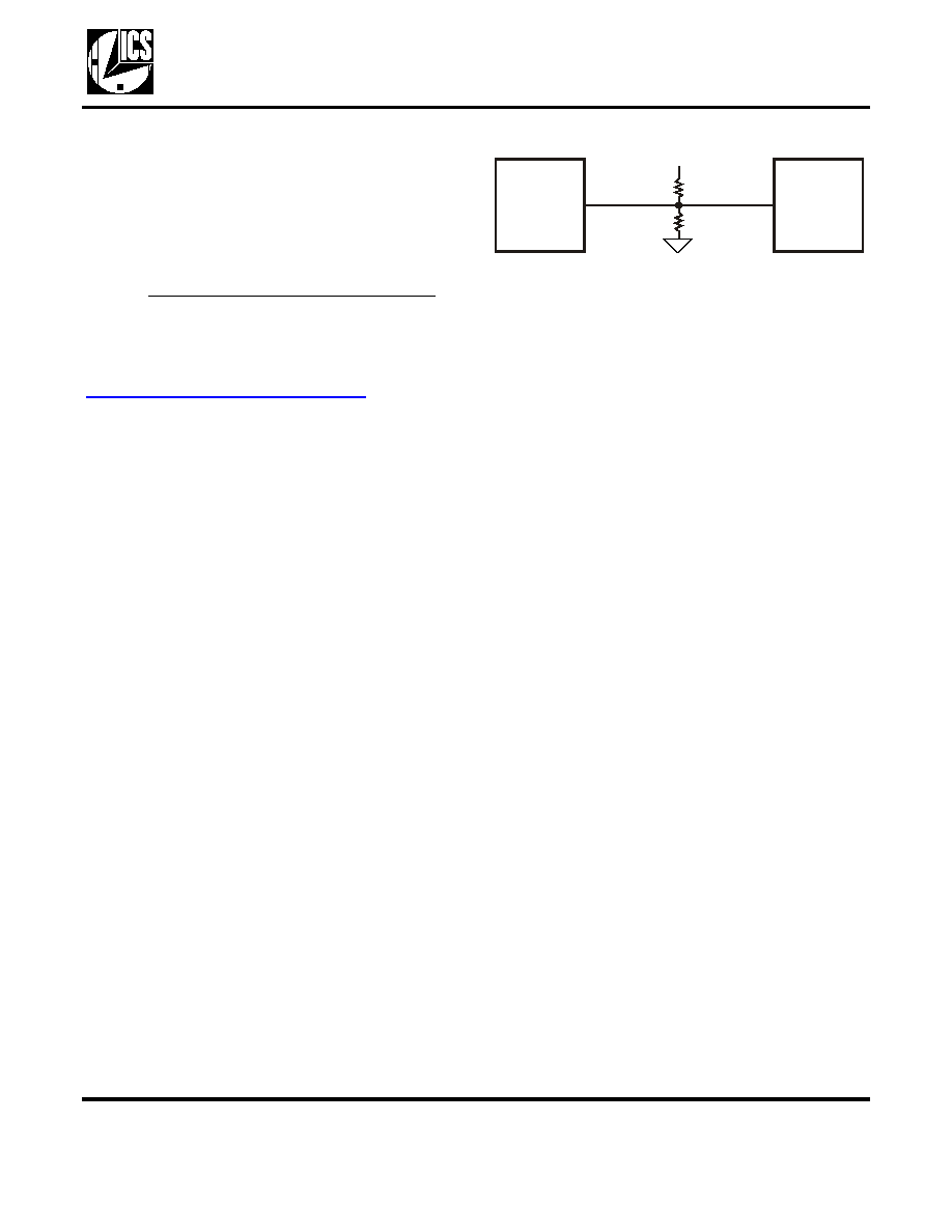
ICS1523
SSTL_3 Output
VDD
150
330
Single
LVTTL
Load

Video Clock Synthesizer with I
2
C Programmable Delay
ICS1523
MDS 1523 Y
12
Revision 110905
Integrated Circuit Systems 525 Race Street, San Jose, CA 95126 tel (408) 297-1201
www.icst.com
Section 11 Programming
11.1 Industry-Standard I
2
C Serial Bus: Data Format
Figure 11-1 ICS1523 Data Format for I
2
C 2-Wire Serial Bus
Note:
∑
1 - Lower nibble of the I
2
C register automatically increments after each successive data byte is written to
or read from the ICS1523.
∑
2 - Upper nibble of the I
2
C register does not automatically increment, and the software must explicitly
re-address the ICS1523. The software:
≠ Must NOT just index 0 and then do all the I/O as one-byte transactions.
≠ Must break the transactions into at least two separate bus transactions:
(1) 00 to 08 (2) 10 to 12
Write Procedure for Single Register
MSB
LSB
S 0 1 0 0 1 1 X 0 A
A
A
Device address
Register Index
Data
Read Procedure for Single Register
MSB
LSB
MSB
LSB
S 0 1 0 0 1 1 X 0 A
A S 0 1 0 0 1 1 X 1 A
A
Device address
Register Index
Device address
Data
Repeat START
NO Acknow ledge
Write Procedure for Multiple Registers (Note 1)
MSB
LSB
S 0 1 0 0 1 1 X 0 A
A
A
A
A
Device address
Register Index
Data
Data
Read Procedure for M ultiple Registers (Note 1)
MSB
LSB
MSB
LSB
S 0 1 0 0 1 1 X 0 A
A S 0 1 0 0 1 1 X 1 A
A
A
Device address
Register Index
Device address
Data
Data
Repeat START
NO Acknow ledge
Legend
All values are sent with the most-significant bit (MSB) first and least-significant bit (LSB) last.
R
= Read = 1
W
= Write = 0
S
= Start (SDA goes low when SCL was high, then SCL goes low too)
A
= ACK = Acknowledge = 0
A
= ACK = No Acknowledge = 1
X
= Bit value that equals logic state of SBADR pin.
= (Dashed Line) Multiple transactions
Bus Master drives signal to ICS1523
ICS1523 (Slave Device) drives signal to Bus Master
Stop
Stop
Stop
Stop

Video Clock Synthesizer with I
2
C Programmable Delay
MDS 1523 Y
13
Revision 110905
Integrated Circuit Systems 525 Race Street, San Jose, CA 95126 tel (408) 297-1201
www.icst.com
ICS1523
11.2 Programming Flow for Modifying PLL and DPA Settings
BEGIN
Determine Horizontal Total
HTOTAL
Program Input Control Register Reg0x0
Typically = 41h
(Coast disabled, Positive edge of HSYNC, Internal Feedback,
FUNC = regenerated HSYNC, PLL lock status to LOCK (STATUS) pin
Program DPA Reg0x5
DPA Resolution 0x5 = (Value From Note 8 Table)
DPA Offset, 0x4:5~0 = 0
Full S/W Reset
Reg0xA = 5Ah
Correct Phase
Relationship?
Decrement Charge
Pump Current
Reg0x1:2~0
END
Program Feedback Divider Reg0x2, Reg0x3
Internal Feedback Divider (0x3 & 0x2) = HTOTAL - 8
Program Loop Control Register Reg0x1
VCO Divider 0x1:5~4 = (Maximum value where
Required Output Frequency * VCOD < 500 MHz)
Typical Charge Pump Current 0x1:2~0= 011b
Program Output Control Reg0x6
Enable the desired outputs
Program OSC Divider Reg0x7
Select Desired Input Reg0x7:7
Select OSC divider value (if needed)
Increment DPA
Offset
Reg0x4
Program Internal Filter Reg0x4
Select Internal Filter 0x4:7 = 1
Yes
Yes
No
PLL LOCKED?
LOCK Pin or
Read 0x12:1
No

Video Clock Synthesizer with I
2
C Programmable Delay
ICS1523
MDS 1523 Y
14
Revision 110905
Integrated Circuit Systems 525 Race Street, San Jose, CA 95126 tel (408) 297-1201
www.icst.com
Section 12 Timing Diagrams
Figure 12-1 DPA Operation
DPA Offset = CLK Period * (# of DPA Elements Selected [0x4:4~0]
(# of DPA Elements Available)[0x5:1-0]
Table 12-1 DPA Offset Ranges
Using the DPA above 160 MHz is not recommended. Set DPA_OS = 0 for speeds in excess of 160 MHz to bypass
the DPA. The DPA Resolution Select register (0x5:0~1) is double-buffered. Working registers are loaded only after
a DPA Software reset (0x8=xA)
Register 5
0x4:5-0
Maximum
DPA Clock Range in MHz
1~0
Total # of DPA
Elements
Selected #
of DPA
Elements
Min
Max
00
16
0F
48
160
01
32
1F
24
80
11
64
3F
12
40
HSYNC
DPA Offset when
DPA_OS [5-0] = 0
.
.
.
One full speed clock period
DPA Offset when
DPA_OS [5-0] = 1
DPA Offset when
DPA_OS [5-0] = 2
DPA Offset when
DPA_OS [5-0] = Max
1 unit of DPA delay
2 units of DPA delay
Maximum units of DPA delay
Fixed delay
- See
Figure 12-2
and
Figure 12-3
1 unit of DPA delay

Video Clock Synthesizer with I
2
C Programmable Delay
MDS 1523 Y
15
Revision 110905
Integrated Circuit Systems 525 Race Street, San Jose, CA 95126 tel (408) 297-1201
www.icst.com
ICS1523
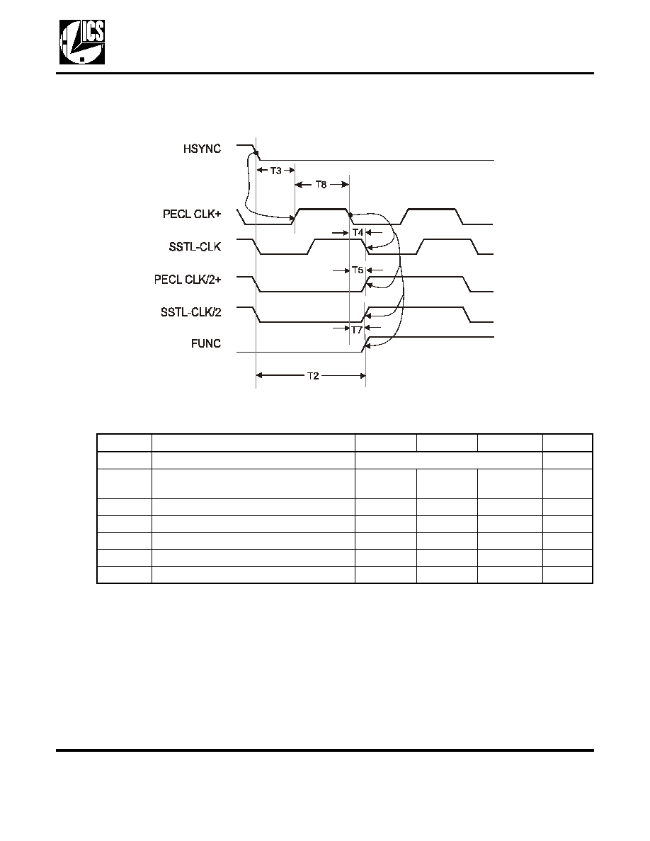
12.1 Timing for 0x0:2=0
Figure 12-2 0x0:2=0 Timing Diagram
Table 12-2
0x0:2=0 Timing Values
Symbol Parameter
Minimum
Typical
Maximum
Units
T2
HSYNC High to FUNC High
(DPA Offset = 0)
T8 + T3
ns
T3
HSYNC High to PECL CLK+ High
(DPA Offset = 0)
-
7
-
ns
T4
PECL Clock Low to SSTL_3 Clock Low
Delay
0
0.2
0.6
ns
T5
PECL Clock Low to FUNC High Delay
0.6
1.0
1.6
ns
T6
PECL Clock Low to PECL/2 High Clock
0.6
1.0
1.6
ns
T7
PECL Clock Low to SSTL_3 CLK/2 Delay
0.4
0.9
1.2
ns
T8
PECL Clock High Time
-
0.5
-
UI
Video Clock Synthesizer with I
2
C Programmable Delay
ICS1523
MDS 1523 Y
16
Revision 110905
Integrated Circuit Systems 525 Race Street, San Jose, CA 95126 tel (408) 297-1201
www.icst.com
12.2 Timing for 0x0:2=1
Figure 12-3 0x0:2=1 Timing Diagram
Table 12-3
0x0:2=1 Timing Values
Symbol Parameter
Minimum
Typical
Maximum
Units
T2
HSYNC Low to FUNC High Delay
T8 + T3
ns
T3
HSYNC Low to PECL CLK+ High Delay
(DPA Offset = 0)
-
10
-
ns
T4
PECL Clock to SSTL_3 Clock Delay
0
0.2
0.6
ns
T5
PECL Clock to FUNC Delay
0.6
1.0
1.6
ns
T6
PECL Clock to PECL/2 Clock
0.6
1.0
1.6
ns
T7
PECL Clock to SSTL_3 CLK/2 Delay
0.4
0.9
1.2
ns
T8
PECL Clock High Time
-
0.5
-
UI

Video Clock Synthesizer with I
2
C Programmable Delay
MDS 1523 Y
17
Revision 110905
Integrated Circuit Systems 525 Race Street, San Jose, CA 95126 tel (408) 297-1201
www.icst.com
ICS1523
12.3 HSYNC to REF Timing
Figure 12-4 HSYNC to REF Timing Diagram
Table 12-4 HSYNC to REF Timing Diagram
12.4 CLK/2 Timing for Odd and Even Feedback Divider
Figure 12-5 CLK/2: Even versus Odd
For simplicity, the waveforms drawn show only the identical PECL CLK/2+ and the SSTL_3 CLK/2 signals. CLK/2-
is the compliment of the CLK/2+ signal.
Note that regardless of the CLK\2 phase at the assertion of FUNC, the clocks always have the same phase at the
fall of FUNC, regardless of 0x2
Symbol Parameter
Minimum
Typical
Maximum
Units
T
0
HSYNC Low to REF Delay
6
7.5
8.5
ns
T
1
HSYNC High to REF Delay
3.5
4.3
6
ns
REF
HSYNC
t
0
Reg0:2 = 1
REF
HSYNC
t1
Reg0:2 = 0
t1
t0
FUNC
CLK/2
Even - Reg2:0=0
CLK/2
Odd - Reg2:0=1

Video Clock Synthesizer with I
2
C Programmable Delay
ICS1523
MDS 1523 Y
18
Revision 110905
Integrated Circuit Systems 525 Race Street, San Jose, CA 95126 tel (408) 297-1201
www.icst.com
Section 13 AC/DC Operating Conditions
13.1 Absolute Maximum Ratings
Table 13-1
lists absolute maximum ratings for the ICS1523. Stresses above these ratings can cause permanent
damage to the device. These ratings, which are standard values for ICS commercially rated parts, are stress
ratings only. Functional operation of the ICS1523 at these or any other conditions above those indicated in the
operational sections of the specifications is not implied. Exposure to absolute maximum rating conditions for
extended periods can affect product reliability. Electrical parameters are guaranteed only over the recommended
operating temperature range.
Table 13-1 ICS1523 Absolute Maximum Ratings
Note: Measured with respect to VSS. During normal operations, the VDD supply voltage for the ICS1523
must remain within the recommended operating conditions.
Table 13-2 Environmental Conditions
Table 13-3 DC Characteristics
Table 13-4 AC Characteristics
Parameter
Min.
Typ.
Max.
Units
Ambient Operating Temperature
0
≠
+70
į C
Power Supply Voltage
+3.0
+3.3
+3.6
V
Parameter
Symbol
Conditions
Min.
Max.
UNITS
Digital Supply Current
IDDD
VDDD=3.6V
-
25
mA
Output Driver Supply Current
IDDQ
VDDD=3.6V
No drivers enabled
-
6
mA
Analog Supply Current
IDDA
VDDA=3.6V
-
5
mA
Parameter
Symbol
Min.
Max.
Units
Notes
AC Inputs
HSYNC Input Frequency
f
HSYNC
15.734
10,000
kHz
0x7:7=1
OSC Input Frequency
f
OSC
0.05
100
MHz
0x7:7=0
PDEN Input Frequency
f
PDEN
30
120
Hz
Internal VCO Frequency
f
VCO
100
500
MHz
Typical Lock Time
t
LOCK
20
ms
Item
Rating
VDD, VDDA, VDDQ (measured to VSS)
4.3 V
Digital Inputs
VSS ≠0.3 V to 5.5 V
Analog Outputs
VSSA ≠0.3 V to VDDA +0.3 V
Digital Outputs
VSSQ ≠0.3 V to VDDQ +0.3 V
Storage Temperature
≠65įC to +150įC
Junction Temperature
125įC
Soldering Temperature
260įC
ESD Susceptibility*
> 2 KV
(*Electrostatic-sensitive devices. Do not open or handle except in a static-free workstation.)

Video Clock Synthesizer with I
2
C Programmable Delay
MDS 1523 Y
19
Revision 110905
Integrated Circuit Systems 525 Race Street, San Jose, CA 95126 tel (408) 297-1201
www.icst.com
ICS1523
Note 1- V
OL
must not fall below the level given so that the correct value for IOUT can be maintained.
Note 2- Measured at 135MHz, 3.6 VDC, 0
o
C, 20 pF, with 75
Termination
Note 3- Measured at 135MHz, 3.6 VDC, 0
o
C, 20 pF, Unterminated
Analog Input (HSYNC)
Input High Voltage
V
IH
1.7
5.5
V
Input Low Voltage
V
IL
VSS - 0.3
1.1
V
Digital Inputs (SDA, SCL, EXTFB, OSC, I
2
CADDR)
Input High Voltage
V
IH
2
5.5
V
Input Low Voltage
V
IL
VSS - 0.3
0.8
V
Input Hysteresis
-
0.2
0.6
V
POR Threshold
-
VSS
1.8
V
Voltage that resets
register values
SDA Digital Output
SDA Output Low Voltage
V
OL
0.4
V
IOUT = 3ma
SDA Output High Voltage
V
OH
6.0
V
Determined by
external Rset
resistor
PECL Outputs (CLK+, CLK-, CLK/2+, CLK/2-)
Output High Voltage
V
OH
-
VDD
V
IOUT=0
Maximum Output Frequency
F
P
MAX
-
250
MHz
VDDD = 3.3 V
Output Low Voltage *
V
OL
1.0
-
V
IOUT =
Programmed Value
1
Duty Cycle
P
DC
45
55
%
2
Transition Time - Rise
T
PR
-
1.0
ns
2
Transition Time - Fall
T
PF
-
1.2
ns
2
SSTL_3 Outputs (CLK, CLK/2, FUNC, LOCK/REF)
Output Resistance
R
O
-
80
1 V < V
O
< 2 V
Maximum Output Frequency
F
s
MAX
-
150
MHz
VDDD = 3.3 V
Duty Cycle
S
DC
45
55
%
3
Clock and FUNC
Transition Time - Rise
T
CR
-
1.6
ns
3
Clock and FUNC
Transition Time - Fall
T
CF
-
1.0
ns
3
LOCK/REF Transition Time -
Rise
T
LR
-
3.0
ns
3
LOCK/REF Transition Time - Fall
T
LF
-
2.0
ns
3
Parameter
Symbol
Min.
Max.
Units
Notes

Video Clock Synthesizer with I
2
C Programmable Delay
ICS1523
MDS 1523 Y
20
Revision 110905
Integrated Circuit Systems 525 Race Street, San Jose, CA 95126 tel (408) 297-1201
www.icst.com
Table 13-5 Thermal Characteristics
Parameter
Symbol
Conditions
Min.
Typ.
Max.
Units
Thermal Resistance Junction to
Ambient
JA
Still Air
67
įC/W
JA
1 m/s air flow
56
įC/W
JA
3 m/s air flow
51
įC/W
Thermal Resistance Junction to
Case
JC
25
įC/W

Video Clock Synthesizer with I
2
C Programmable Delay
MDS 1523 Y
21
Revision 110905
Integrated Circuit Systems 525 Race Street, San Jose, CA 95126 tel (408) 297-1201
www.icst.com
ICS1523
Section 14 Package Dimensions
Figure 14-1 Physical Dimensions for
ICS1523
Section 15 Ordering Information
Note: "LF" denotes Pb (lead) free package.
While the information presented herein has been checked for both
accuracy and reliability, Integrated Circuit Systems, Incorporated
(ICS) assumes no responsibility for either its use or for infringement
of any patents or other rights of third parties, which would result from
its use. No other circuits, patents, or licenses are implied. This
product is intended for use in normal commercial applications. Any
other applications such as those requiring extended temperature
range, high reliability, or other extraordinary environmental
requirements are not recommended without additional processing by
ICS. ICS reserves the right to change any circuitry or specifications
without notice. ICS does not authorize or warrant any ICS product for
use in life support devices or critical medical instruments
L Ī .008
0.029
Typ.
0.018
0.296 Ī 0.005
0.047R
Pin 1
5 Deg. Typ.
5 Deg. Typ. Ī 5
0.328 Ī 0.010
0.406 Ī 0.010
0.015 x 45 Deg.
0.020
0.010
5 Deg Typ.
0.092 Ī 0.005
0.041 Ī 0.003
0.050
Pitch Typ.
0.008 Ī 0.006
0.101 Ī 0.010
24-pin SOIC (300 Mil Wide Body)
Part / Order Number
Marking
Package
Shipping Package
Temperature
ICS1523M
ICS1523M
24-pin SOIC
Tubes
0 to 70
įC
ICS1523MT
ICS1523M
24-pin SOIC
Tape and Reel
0 to 70
įC
ICS1523MLF
ICS1523MLF
24-pin SOIC
Tubes
0 to 70
įC
ICS1523MLFT
ICS1523MLF
24-pin SOIC
Tape and Reel
0 to 70
įC