
MDS 1527 G
Revision 110905
ICS reserves the right to make changes in the preliminary device data
identified in this publication without notice. ICS advises its customers
to obtain the latest version of all device data to verify that information
being relied upon is current and accurate.
Integrated Circuit Systems
ICS1527
Video Clock Synthesizer
Features
∑ Lead-free packaging (Pb-free)
∑ Low jitter (typical 27 ps short term jitter)
∑ LVCMOS single-ended clock outputs
∑ 60/110 MHz speed grades available
∑ Uses 3.3 V power supply
∑ 5 Volt tolerant Inputs (HSYNC, VSYNC)
∑ Coast (ignore HSYNC) capability via VSYNC pin
∑ Industry standard I
2
C-bus programming interface
∑ PLL Lock detection via I
2
C or LOCK output pin
∑ 16-pin TSSOP package
Applications
∑ Frequency synthesis
∑ LCD monitors, video projectors and plasma displays
∑ Genlocking multiple video subsystems
Pin Configuration (16-pin TSSOP)
VDDD
1
VSSD
SDA
SCL
VSYNC
I2CADR
VDDA
VSSQ
VDDQ
CLK
HSYNC_out
LOCK
VSYNC_out
HSYNC
VSSA
2
3
4
5
6
7
8
9
10
11
12
13
14
15
16
EXTFB
General Description
The ICS1527 is a low-cost, high-performance
frequency generator. It is suited to general purpose
phase controlled clock synthesis as well as
line-locked and genlocked high-resolution video
applications. Using ICS's advanced low-voltage
CMOS mixed-mode technology, the ICS1527 is an
effective clock synthesizer that supports video
projectors and displays at resolutions from VGA to
beyond XGA.
The ICS1527 offers single-ended clock outputs to 60
or 110 MHz. The HSYNC_out, and VSYNC_out pins
provide the regenerated versions of the HSYNC and
VSYNC inputs synchronous to the CLK output.
The advanced PLL uses either its internal
programmable feedback divider or an external divider.
The device is programmed by a standard I
2
C-busTM
serial interface and is available in a TSSOP16
package.
ICS1527 Functional Diagram
HSYNC
VSYNC
I
2
C
HSYNC_out
VSYNC_out
EXTFB
External
Divider
CLK
ICS1527
MDS 1527 G
2
Revision 110905
Integrated Circuit Systems, 525 Race Street, San Jose, CA 95126, tel (408) 297-1201
www.icst.com
Section 1 Overview
ICS1527 Data Sheet
Section 1 Overview
The ICS1527 is a user-programmable,
high-performance general purpose clock generator. It
is intended for graphics system line-locked and
genlocked applications, and provides the clock signals
required by high-performance analog-to-digital
converters.
The ICS1527 has the ability to operate in line-locked
mode with the HSYNC input.
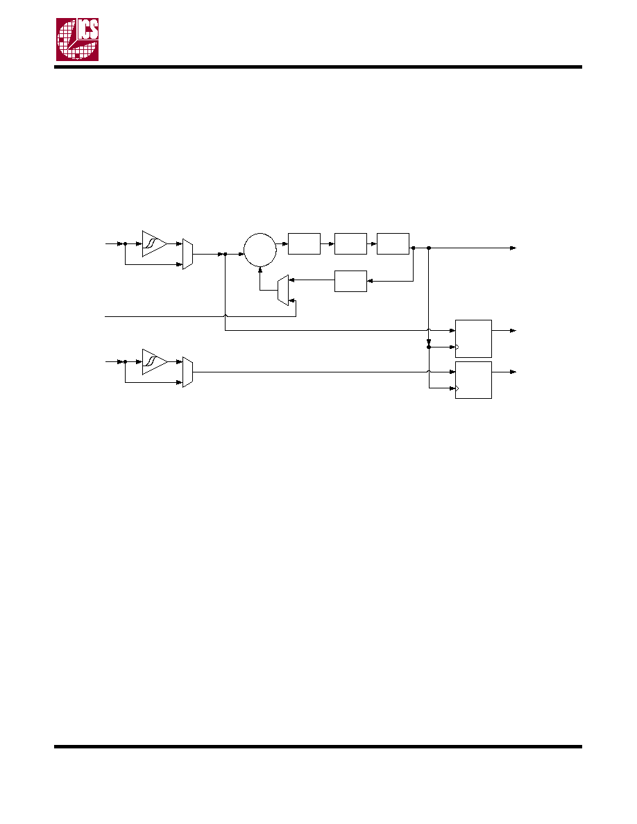
1.1 Phase-Locked Loop
The phase-locked loop has a very wide input frequency
range (8 kHz to 100 MHz). Not only is the ICS1527 an
excellent, general purpose clock synthesizer, but it is
also capable of line-locked operation. Refer to the
block diagram below.
The heart of the ICS1527 is a voltage controlled
oscillator (VCO). The VCO speed is controlled by the
voltage on the loop filter. This voltage will be described
later in this section.
The VCO's clock output is first passed through the
VCO Divider (VCOD). The VCOD allows the VCO to
operate at higher speeds than the required output
clock.
NOTE: Under normal, locked operation the VCOD has
no effect on the speed of the output clocks, just the
VCO frequency.
The output of the VCOD is the full speed output
frequency seen on the CLK. This clock is then sent
through the 12-bit internal Feedback Divider (FD). The
feedback divider controls how many clocks are seen
during every cycle of the input reference.
The Phase Frequency Detector (PFD) then compares
the feedback to the input and controls the filter voltage
by enabling and disabling the charge pump. The
charge pump has programmable current drive and will
source and sink current as appropriate to keep the
input and the HSYNC_out output aligned.
The input HSYNC and VSYNC can be conditioned by a
high-performance Schmitt-trigger by sharpening the
rising/falling edge.
The HSYNC_out and VSYNC_out signals are aligned
with the output clock (CLK) via a set of flip flops.
1.2 Output Drivers and Logic Inputs
The ICS1527 uses low-voltage TTL (LVTTL) inputs and
LVCMOS outputs, operating at the 3.3 V supply
voltage. The LVTTL inputs are 5 V tolerant.
The LVCMOS drive resistive terminations or
transmission lines.
1.3 Automatic Power-On Reset Detection
The ICS1527 has automatic power-on reset detection
(POR) circuitry and it resets itself if the supply voltage
drops below threshold values. No external connection
to a reset signal is required.
Figure 1-1 Simplified Block Diagram
Note: Polarity controls and other circuit elements are not shown in above diagram for simplicity
PFD
CP
VCO
VCOD
2,4,8,16
HSYNC
Flip-flop
VSYNC
CLK
HSYNC_out
VSYNC_out
FD
12..4103
Flip-flop
EXTFB

MDS1527 G
3
Revision 110905
Integrated Circuit Systems, 525 Race Street, San Jose, CA 95126, tel (408) 297-1201
www.icst.com
Section 1 Overview
ICS1527 Data Sheet
1.4 I
2
C Bus Serial Interface
The ICS1527 uses a 5 volt tolerant, industry-standard
I
2
C-bus serial interface that runs at either low-speed
(100 kHz) or high-speed (400 kHz). The interface uses
12 word addresses for control and status: one
write-only, eight read/write, and three read-only
addresses.
Two ICS1527 devices can sit on the same I
2
C bus,
each selected by the Master according to the state of
the I2CADR pin. The 7 bit device address is 0100110
(binary) when I2CADR is low. The device address is
0100111 (binary) when I2CADR is high. See
Section 4,
"Programming"

MDS 1527 G
4
Revision 110905
Integrated Circuit Systems, 525 Race Street, San Jose, CA 95126, tel (408) 297-1201
www.icst.com
Section 2 Pin Descriptions
ICS1527 Data Sheet
Section 2 Pin Descriptions
Notes: 1. These LVTTL inputs are 5 V tolerant.
2. Connect to ground if unused.
Table 2-1
ICS1527
Pin Descriptions
PIN NO. PIN NAME
TYPE
DESCRIPTION
COMMENTS
Notes
1
VSSD
POWER
Digital ground
2
SDA
IN/OUT
Serial data
I
2
C-bus
1
3
SCL
IN
Serial clock
I
2
C-bus
1
4
VSYNC
IN
Vertical sync
1 & 2
5
EXTFB
IN
External feedback
From External Divider
1 & 2
6
HSYNC
IN
Horizontal sync
Clock input to PLL
1 & 2
7
VDDA
POWER
Analog supply
Power for analog circuitry
8
VSSA
POWER
Analog ground
Ground for analog circuitry
9
I2CADR
IN
I
2
C device address
Chip I
2
C address select
10
LOCK
LVCMOS
OUT
Lock
PLL lock
11
HSYNC_out
LVCMOS
OUT
HSYNC output
Schmitt-trigger filtered HSYNC
realigned with the output pixel clock
12
CLK
LVCMOS
OUT
Pixel clock output
LVCMOS driver for full-speed clock
13
VDDQ
POWER
Output driver supply
Power for output drivers
14
VSYNC_out
LVCMOS
OUT
VSYNC output
Schmitt-trigger filtered VSYNC
realigned with the output pixel clock
15
VSSQ
POWER
Output driver ground
Ground for output drivers
16
VDDD
POWER
Digital supply
Power for digital sections

MDS1527 G
5
Revision 110905
Integrated Circuit Systems, 525 Race Street, San Jose, CA 95126, tel (408) 297-1201
www.icst.com
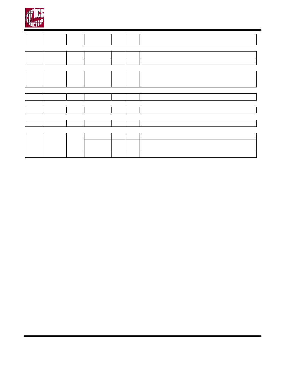
Section 3 Register map summary
ICS1527 Data Sheet
Section 3 Register map summary
Word
Address
Name
Access
Bit Name
Bit #
Reset
Value
Description
00h
Input
Control
R / W
CPen
0
1
Charge Pump Enable
0=External Enable via VSYNC, 1=Always Enabled
VSYNC_Pol
1
0
VSYNC Polarity (Charge Pump Enable)
Requires 00h:0=0
0=Coast (charge pump disabled) while VSYNC low,
1=Coast (charge pump disabled) while VSYNC high
HSYNC_Pol
2
0
HSYNC Polarity
0=Rising Edge, 1=Falling Edge
Fbk_Pol
3
0
External Feedback Polarity
0=Positive Edge, 1=Negative Edge
Fbk_Sel
4
0
External Feedback Select
0=Internal Feedback, 1=External
Reserved
5
0
Reserved
EnPLS
6
1
Enable PLL Lock Status Output
0=Disable, 1=Enable
Reserved
7
0
Reserved
01h
Loop
Control
*
R / W
ICP0-2
0-2
ICP (Charge Pump Current)
Bit 2,1,0 = {000 =1
µA, 001 = 2 µA, 010 = 4 µA... 110 = 64 µA, 111 =
128
µA}. Increasing the PF Detector Gain makes the loop respond
faster, raising the loop bandwidth. The typical value when using the
internal loop filter is 011.
Reserved
3
Reserved
VCOD0-1
4-5
VCO Divider
Bit 5,4= {00 = ˜2, 01=˜4, 10=˜8, 11=˜16}
Reserved
6-7
Reserved
02h
FdBk Div
0
*
R / W
FBD0-7
0-7
Feedback Divider LSBs (bits 0-7)
03h
FdBk Div
1
*
R / W
FBD8-11
0-3
Feedback Divider MSBs (bits 8-11)
Divider setting = 12 bit word + 8
Minimum 12 = 000000000100
Maximum 4103 =111111111111
Reserved
4-7
Reserved
04h
Reserved
Reserved
0-7
0
Reserved
05h
Schmitt-
trigger
*
R / W
Schmitt
control
0
1
Schmitt-trigger control
0=Schmitt-trigger, 1=No Schmitt-trigger
Metal_Rev
1-7
0
Metal Mask Revision Number
06h
Output
Enables
R / W
Reserved
0
0
Reserved
OE
1
0
Output Enable for CLK, HSYNC_out, VSYNC_out
0=High Impedance (disabled), 1=Enabled
Reserved
2-7
0
Reserved
MDS 1527 G
6
Revision 110905
Integrated Circuit Systems, 525 Race Street, San Jose, CA 95126, tel (408) 297-1201
www.icst.com
Section 3 Register map summary
ICS1527 Data Sheet
07h
Reserved
Reserved
0-6
Reserved
Reserved
7
0
Part requires a 0 for correct operation
08h
Reset
Write
Reserved
0-7
0
Writing 5Ah resets part and commits values written to word
addresses 01h-03h and 05h
09-0Fh
Reserved
Read
Reserved
0-7
Reserved
10h
Chip Ver
Read
Reserved
0-7
Reserved
11h
Chip Rev
Read
Chip Rev
0-7
01
Reserved
12h
Rd_Reg
Read
Reserved
0
N/A
Reserved
PLL_Lock
1
N/A
PLL Lock Status
0=Unlocked, 1=Locked
Reserved
2-7
0
Reserved
*. Written values to these registers do not take effect immediately, but require a commit via register 08h
Word
Address
Name
Access
Bit Name
Bit #
Reset
Value
Description
MDS1527 G
7
Revision 110905
Integrated Circuit Systems, 525 Race Street, San Jose, CA 95126, tel (408) 297-1201
www.icst.com
Section 4 Programming
ICS1527 Data Sheet
Section 4 Programming
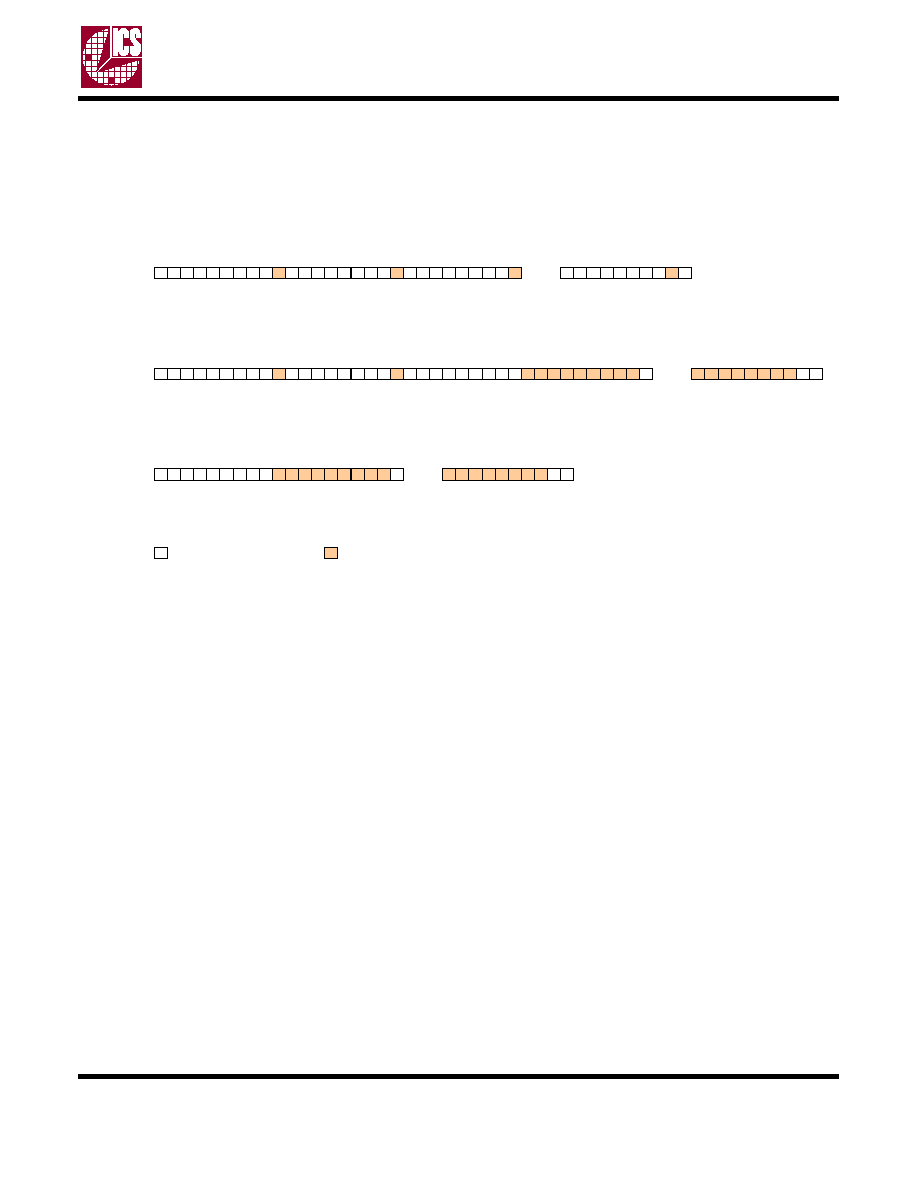
4.1 Industry-Standard I
2
C Serial Bus: Data Format
Figure 4-1 ICS1527 Data Format for I
2
C 2-Wire Serial Bus
Notes:
The ICS1527 uses 16 byte pages (00h-0Fh is the first page, 10h-1Fh is the second page). Writing or reading
beyond the end of page yields undefined results.
The ICS1527 has a device address of 010011B, where B is the state of the I2CADR pin.
S
T
A
R
T
0 A
C
K
A
C
K
A
C
K
Single/m ultiple register w rite (page w rite)
W ord address
D ata (0)
A
C
K
D ata (n)
S
T
O
P
...
S
T
A
R
T
0 A
C
K
A
C
K
A
C
K
S ingle/m ultiple register read
W ord address
D ata (0)
D ata (n)
S
T
O
P
...
1 A
C
K
N
O
A
C
K
S
T
A
R
T
A
C
K
S equential single/m ultiple register read
D ata (0)
D ata (n)
S
T
O
P
...
1 A
C
K
N
O
A
C
K
S
T
A
R
T
0 1 0 0 1 1 B
D evice address
D evice address
D evice address
D evice address
0 1 0 0 1 1 B
0 1 0 0 1 1 B
0 1 0 0 1 1 B
M aster drives line
S lave drives line
MDS 1527 G
8
Revision 110905
Integrated Circuit Systems, 525 Race Street, San Jose, CA 95126, tel (408) 297-1201
www.icst.com
Section 5 AC/DC Operating Conditions
ICS1527 Data Sheet
Section 5 AC/DC Operating Conditions
5.1 Absolute Maximum Ratings
Table 5-1
lists absolute maximum ratings for the ICS1527. Stresses above these ratings can cause permanent
damage to the device. These ratings, which are standard values for ICS commercially rated parts, are stress ratings
only. Functional operation of the ICS1527 at these or any other conditions above those indicated in the operational
sections of the specifications is not implied. Exposure to absolute maximum rating conditions for extended periods
can affect product reliability. Electrical parameters are guaranteed only over the recommended operating
temperature range.
Table 5-2 Environmental Conditions
Table 5-3 DC Characteristics
Table 5-1 ICS1527 Absolute Maximum Ratings
Item
Rating
VDD, VDDA, VDDQ (measured to VSS)
*
*. Measured with respect to VSS. During normal operations, the VDD supply voltage for the ICS1527 must
remain within the recommended operating conditions.
4.3 V
Digital Inputs
VSS ≠0.3 V to 5.5 V
Analog Inputs
VSS -0.3 V to 6.0 V
Analog Outputs
VSSA ≠0.3 V to VDDA +0.3 V
Digital Outputs
VSSQ ≠0.3 V to VDDQ +0.3 V
Storage Temperature
≠65∞C to +150∞C
Junction Temperature
125∞C
Soldering Temperature
260∞C
ESD Susceptibility*
> 2 KV
**
**. Electrostatic-sensitive devices. Do not open or handle except in a static-free workstation.
Parameter
Min.
Typ.
Max.
Units
Ambient Operating Temperature
0
≠
+70
∞ C
Power Supply Voltage
+3.0
+3.3
+3.6
V
Parameter
Symbol
Conditions
Min.
Max.
UNITS
Digital Supply Current
IDDD
VDDD = 3.6 V
-
25
mA
Output Driver Supply Current
IDDQ
VDDD = 3.6 V
No drivers enabled
-
6
mA
Analog Supply Current
IDDA
VDDA = 3.6 V
-
5
mA
Power consumption
300
mW
Power-On-Reset (POR)
Threshold
VSS
1.8
V

MDS1527 G
9
Revision 110905
Integrated Circuit Systems, 525 Race Street, San Jose, CA 95126, tel (408) 297-1201
www.icst.com
Section 5 AC/DC Operating Conditions
ICS1527 Data Sheet
Table 5-4 AC Characteristics
Parameter
Symbol
Min.
Typical
Max.
Units
Notes
General
VCO Frequency
f
VCO
50
400
MHz
VCO Gain
K
165
MHz/V
AC Inputs
EXTFB Input Frequency
f
EXTFB
8
10,000
kHz
EXTFB Input High Voltage
V
IH
2.0
V
EXTFB Input Low Voltage
V
IL
1.0
V
Analog Input (HSYNC/VSYNC)
HSYNC Input Frequency
f
HSYNC
8
10,000
kHz
VSYNC Input Frequency
f
VSYNC
30
120
Hz
Input High Voltage
V
IH
1.7
5.5
V
Input Low Voltage
V
IL
VSS - 0.3
1.1
V
Input Hysteresis
0.2
0.8
V
Schmitt trigger active
SDA, SCL Digital Inputs
Input High Voltage
V
IH
2
5.5
V
Input Low Voltage
V
IL
VSS - 0.3
0.8
V
I
2
CADDR Digital Input
Input High Voltage
V
IH
2
VDD+0.3
V
Input Low Voltage
V
IL
VSS - 0.3
0.8
V
SDA Digital Output
SDA Output Low Voltage
V
OL
0.4
V
IOUT = 3 mA
SDA Output High Voltage
V
OH
6.0
V
Determined by
external Rset resistor
LVCMOS Outputs (CLK, HSYNC_out, VSYNC_out, LOCK)
Output Frequency,
ICS1527-110GLF
F
s
2.5
110
MHz
VDDD = 3.3 V
Output Frequency,
ICS1527-60GLF
F
s
2.5
60
MHz
VDDD = 3.3 V
Duty Cycle
S
DC
45
50
55
%
2
Jitter, STJ, RMS
STJ
0.027
ns
30 kHz input to 50
MHz output
Jitter, STJ, pk-pk
STJ
0.200
ns
Jitter, Input-Output
IOJ
2.500
ns
HSYNC in to CLK out
Output Low Voltage
V
OL
0.4
V
IOUT = 4 mA
Output High Voltage
V
OH
2.4
V
IOUT = -4 mA
HSYNC to HSYNC_out
propagation delay (without
Schmitt-trigger)
2
9
ns
1

MDS 1527 G
10
Revision 110905
Integrated Circuit Systems, 525 Race Street, San Jose, CA 95126, tel (408) 297-1201
www.icst.com
Section 5 AC/DC Operating Conditions
ICS1527 Data Sheet
Note 1--Measured between chosen edge of HSYNC (00h:2) and rising edge of output
Note 2--Measured at 110 MHz, 3.3 VDC, 25
o
C, 15 pF, unterminated
HSYNC to HSYNC_out
propagation delay (with
Schmitt-trigger)
6
10
ns
1
CLK to HSYNC_out/
VSYNC_out skew
1.0
ns
Clock and
HSYNC_out/VSYNC_out
Transition Time - Rise
T
CR
1.0
1.5
ns
2
Clock and
HSYNC_out/VSYNC_out
Transition Time - Fall
T
CF
1.0
1.5
ns
2
LOCK Transition Time - Rise
T
LR
3.0
ns
2
LOCK Transition Time - Fall
T
LF
2.0
ns
2
Parameter
Symbol
Min.
Typical
Max.
Units
Notes
MDS1527 G
11
Revision 110905
Integrated Circuit Systems, 525 Race Street, San Jose, CA 95126, tel (408) 297-1201
www.icst.com
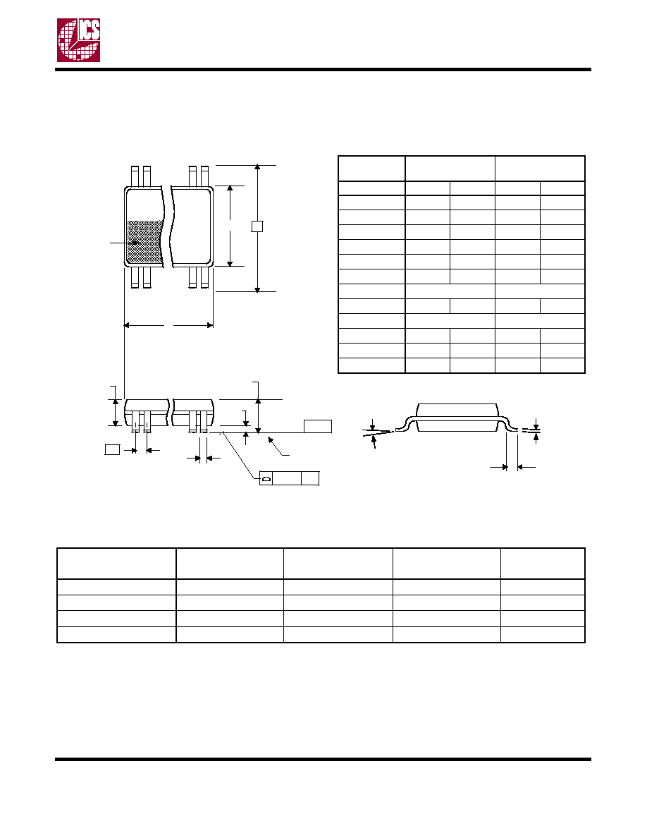
Section 6 Package Outline and Package Dimensions
ICS1527 Data Sheet
Section 6 Package Outline and Package Dimensions
16-pin TSSOP
4.40 mm body, 0.65 mm pitch
Package dimensions are kept current with JEDEC Publication No. 95
Section 7 Ordering Information
While the information presented herein has been checked for both accuracy and reliability, Integrated Circuit Systems (ICS)
assumes no responsibility for either its use or for the infringement of any patents or other rights of third parties, which would
result from its use. No other circuits, patents, or licenses are implied. This product is intended for use in normal commercial
applications. Any other applications such as those requiring extended temperature range, high reliability, or other extraordinary
environmental requirements are not recommended without additional processing by ICS. ICS reserves the right to change any
circuitry or specifications without notice. ICS does not authorize or warrant any ICS product for use in life support devices or
critical medical instruments.
Part / Order Number
Marking
Shipping
packaging
Package
Temperature
ICS1527G-60LF
1527G2LF
Tubes
16-pin TSSOP
0 to +70
∞ C
ICS1527G-60LFT
1527G2LF
Tape & Reel
16-pin TSSOP
0 to +70
∞ C
ICS1527G-110LF
1527G1LF
Tubes
16-pin TSSOP
0 to +70
∞ C
ICS1527G-110LFT
1527G1LF
Tape & Reel
16-pin TSSOP
0 to +70
∞ C
INDEX
AREA
1 2
16
D
E1
E
SEATING
PLANE
A1
A
A2
e
- C -
b
aaa
C
c
L
Millimeters
Inches
Symbol
Min
Max
Min
Max
A
--
1.20
--
0.047
A1
0.05
0.15
0.002
0.006
A2
0.80
1.05
0.032
0.041
b
0.19
0.30
0.007
0.012
C
0.09
0.20
0.0035
0.008
D
4.90
5.1
0.193
0.201
E
6.40 BASIC
0.252 BASIC
E1
4.30
4.50
0.169
0.177
e
0.65 Basic
0.0256 Basic
L
0.45
0.75
0.018
0.030
0
∞
8
∞
0
∞
8
∞
aaa
--
0.10
--
0.004