ICS1572-101 Pinout
ICS1572-301 Pinout
CRYSTAL
OSCILLATOR
/ R
PHASE-
FREQUENCY
DETECTOR
CHARGE
PUMP
LOOP
FILTER
VCO
PRESCALER
/ A
/ M
MUX
MUX
/ 2
/ 4
/ N1
MUX
DRIVER
DIFF.
OUTPUT
DRIVER
/ N2
PROGRAMMING
INTERFACE
CLK+
CLK
-
LOAD
LD/N2
XTAL1
XTAL2
FEEDBACK DIVIDER
EXTFBK
BLANK
(-301 only)
N.C.
1
20
N.C.
AD0
2
19
AD1
XTAL1
3
18
AD2
XTAL2
4
17
VDD
STROBE
5
16
VDD
VSS
6
15
VDDO
VSS
7
14
IPRG
LOAD
8
13
CLK+
LD/N2
9
12
CLK-
N.C.
10
11
N.C.
Description
The ICS1572 is a high performance monolithic phase-locked
loop (PLL) frequency synthesizer. Utilizing ICS's advanced
CMOS mixed-mode technology, the ICS1572 provides a low
cost solution for high-end video clock generation in worksta-
tions and high-end PC applications.
The ICS1572 has differential video clock outputs (CLK+ and
CLK-) that are compatible with industry standard video DACs.
Another clock output, LOAD, is provided whose frequency is
derived from the main clock by a programmable divider. An
additional clock output is available, LD/N2, which is derived
from the LOAD frequency and whose modulus may also be
programmed.
Operating frequencies are fully programmable with direct con-
trol provided for reference divider, pre-scaler, feedback divider
and post-scaler.
Reset of the pipeline delay on Brooktree RAMDACs
may
be performed under register control. Outputs may also be set
to desired states to facilitate circuit board testing.
Features
�
Supports high-resolution graphics - CLK output to
180 MHz
�
Eliminates need for multiple ECL output crystal oscillators
�
Fully programmable synthesizer capability - not just a
clock multiplier
�
Available in 20-pin 300-mil wide body SOIC package
�
Available in both parallel (101) and serial (301)
programming versions
�
Circuit included for reset of Brooktree RAMDAC pipeline
delay
Applications
�
Workstations
�
AutoCad Accelerators
�
High-end PC graphics systems
User Programmable Differential Output Graphics Clock Generator
ICS1572
Figure 1
ICS1572RevC093094
RAMDAC is a trademark of Brooktree Corporation.
Integrated
Circuit
Systems, Inc.
N.C.
1
20
N.C.
AD0
2
19
AD1
XTAL1
3
18
AD2
XTAL2
4
17
VDD
STROBE
5
16
VDD
VSS
6
15
VDDO
VSS
7
14
IPRG
LOAD
8
13
CLK+
LD/N2
9
12
CLK-
N.C.
10
11
N.C.

Overview
The ICS1572 is ideally suited to provide the graphics system
clock signals required by high-performance video DACs.
Fully programmable feedback and reference divider capability
allow virtually any frequency to be generated, not just simple
multiples of the reference frequency. The ICS1572 uses the
latest generation of frequency synthesis techniques developed
by ICS and is completely suitable for the most demanding
video applications.
PLL Synthesizer Description -
Ratiometric Mode
The ICS1572 generates its output frequencies using phase-
locked loop techniques. The phase-locked loop (or PLL) is a
closed-loop feedback system that drives the output frequency
to be ratiometrically related to the reference frequency pro-
vided to the PLL (see Figure 1). The reference frequency is
generated by an on-chip crystal oscillator or the reference
frequency may be applied to the ICS1572 from an external
frequency source.
The phase-frequency detector shown in the block diagram
drives the voltage-controlled oscillator, or VCO, to a frequency
that will cause the two inputs to the phase-frequency detector
to be matched in frequency and phase. This occurs when:
F(XTAL1) . Feedback Divider
F(
VCO)
: =
Reference Divider
This expression is exact; that is, the accuracy of the output
frequency depends solely on the reference frequency provided
to the part (assuming correctly programmed dividers).
The VCO gain is programmable, which permits the ICS1572 to
be optimized for best performance at all operating frequencies.
The reference divider may be programmed for any modulus
from 1 to 128 in steps of one.
The feedback divider may be programmed for any modulus
from 37 through 391 in steps of one. Any even modulus from
392 through 782 can also be achieved by setting the "double"
bit which doubles the feedback divider modulus. The feedback
divider makes use of a dual-modulus prescaler technique that
allows the programmable counters to operate at low speed
without sacrificing resolution. This is an improvement over
conventional fixed prescaler architectures that typically im-
pose a factor-of-four penalty (or larger) in this respect.
Table 1 permits the derivation of "A" & "M" counter program-
ming directly from desired modulus.
PLL Post-Scaler
A programmable post-scaler may be inserted between the VCO
and the CLK+ and CLK- outputs of the ICS1572. This is useful
in generating of lower frequencies, as the VCO has been
optimized for high-frequency operation.
The post-scaler allows the selection of:
�
VCO frequency
�
VCO frequency divided by 2
�
VCO frequency divided by 4
�
Internal register bit (AUXCLK) value
Load Clock Divider
The ICS1572 has an additional programmable divider
(referred to in Figure 1 as the N1 divider) that is used to
generate the LOAD clock frequency for the video DAC. The
modulus of this divider may be set to 3, 4, 5, 6, 8, or 10 under
register control. The design of this divider permits the output
duty factor to be 50/50, even when an odd modulus is selected.
The input frequency to this divider is the output of the PLL
post-scaler described above.
Digital Inputs - ICS1572-101 Option
The AD0-AD3 pins and the STROBE pin are used to load all
control registers of the ICS1572 (-101 option). The AD0-AD3
and STROBE pins are each equipped with a pull-up and will
be at a logic HIGH level when not connected. They may be
driven with standard TTL or CMOS logic families.
The address of the register to be loaded is latched from the
AD0-AD3 pins by a negative edge on the STROBE pin. The
data for that register is latched from the AD0-AD3 pins by a
positive edge on the STROBE pin. See Figure 2 for a timing
diagram. After power-up, the ICS1572-101 requires 32 regis-
ter writes for new programming to become effective. Since
only 13 registers are used at present, the programming system
can perform 19 "dummy" writes to address 13 or 14 to com-
plete the sequence.
ICS1572
2
Digital Inputs - ICS1572-301 Option
The programming of the ICS1572-301 is performed serially
by using the DATCLK, DATA, and HOLD~pins to load an
internal shift register.
DATA is shifted into the register on the rising edge of
DATCLK. The logic value on the HOLD~ pin is latched at the
same time. When HOLD~ is low, the shift register may be
loaded without disturbing the operation of the ICS1572. When
high, the shift register outputs are transferred to the control
registers, and the new programming information becomes ac-
tive. Ordinarily, a high level should be placed on the HOLD~
pin when the last data bit is presented. See Figure 3 for the
programming sequence.
An additional control pin on the ICS1572-301, BLANK can
perform either of two functions. It may be used to disable the
phase-frequency detector in line-locked applications. Alterna-
tively, the BLANK pin may be used as a synchronous enable
for VRAM shift clock generation. See sections on Line-Locked
Operations and VRAM shift clock generation for details.
Output Description
The differential output drivers, CLK+ and CLK, are current-
mode and are designed to drive resistive terminations in a
complementary fashion. The outputs are current-sinking only,
with the amount of sink current programmable via the IPRG
pin. The sink current, which is steered to either CLK+ or CLK-,
is approximately four times the current supplied to the IPRG
pin. For most applications, a resistor from VDDO to IPRG will
set the current to the necessary precision. See Figure 6 for
output characteristics.
The LOAD output is a high-current CMOS type drive whose
frequency is controlled by a programmable divider that may be
selected for a modulus of 3, 4, 5, 6, 8, or 10. It may also be
suppressed under register control.
The LD/N2 output is high-current CMOS type drive whose
frequency is derived from the LOAD output. The programma-
ble modulus may range from 1 to 512 in steps of one.
Pipeline Delay Reset Function
The ICS1572 implements the clocking sequence required to
reset the pipeline delay on Brooktree RAMDACs. This se-
quence can be generated by setting the appropriate register bit
(DACRST) to a logic 1 and then resetting to logic 0.
When changing frequencies, it is advisable to allow 500 mi-
croseconds after the new frequency is selected to activate the
reset function. The output frequency of the synthesizer should
be stable enough at that point for the video DAC to correctly
execute its reset sequence. See Figure 4 for a diagram of the
pipeline delay reset sequence.
This allows the synthesizer to be completely programmed for
the desired frequency before it is made active. Once the part
has been "unlocked" by the 32 writes, programming becomes
effective immediately.
ALL registers identified in the data sheet (0-9, 11, 12 & 15)
MUST be written upon initial programming. The programming
registers are not initialized upon power-up, but the latched
outputs of those registers are. The latch is made transparent
after 32 register writes. If any register has not been written, the
state upon power-up (random) will become effective. Registers
13 & 14 physically do not exist. Register 10 does exist, but is
reserved for future expansion. To insure compatibility with
possible future modifications to the database, ICS recommends
that all three unused locations be written with zero.
Figure 2
8
6
7
DATCLK
DATA
HOLD
DATA_1
DATA_2
DATA_56
ICS1572-301 Register Loading
Figure 3
Pipeline Delay Reset Timing
STROBE
or
DATCLK
CLK+
LOAD
10
9
11
12
T
CLK
Figure 4
5
4
2
1
3
DATA VALID
ADDRESS VALID
AD0-AD3
STROBE
ICS1572-101 Register Loading
ICS1572
3

Reference Oscillator and Crystal
Selection
The ICS1572 has circuitry on-board to implement a Pierce
oscillator with the addition of only one external component, a
quartz crystal. Pierce oscillators operate the crystal in anti-
(also called parallel-) resonant mode. See the AC Charac-
teristics for the effective capacitive loading to specify when
ordering crystals.
Series-resonant crystals may also be used with the ICS1572.
Be aware that the oscillation frequency will be slightly higher
than the frequency that is stamped on the can (typically 0.025-
0.05%).
As the entire operation of the phase-locked loop depends on
having a stable reference frequency, we recommend that the
crystal be mounted as closely as possible to the package. Avoid
routing digital signals or the ICS1572 outputs underneath or
near these traces. It is also desirable to ground the crystal can
to the ground plane, if possible.
If an external reference frequency source is to be used with the
ICS1572, it is important that it be jitter-free. The rising and
falling edges of that signal should be fast and free of noise for
best results.
The loop phase is locked to the falling edges of the XTAL1
input signals.
Line-Locked Operation
The ICS1572 supports line-locked clock applications by al-
lowing the LOAD (N1) and N2 divider chains to act as the
feedback divider for the PLL.
The N1 and N2 divider chains allow a much larger modulus to
be achieved than the PLL's own feedback divider. Additionally,
the output of the N2 counter is accessible off-chip for perform-
ing horizontal reset of the graphics system, where necessary.
This mode is set under register control (ALTLOOP bit). The
reference divider (R counter) is set to divide by 1 in this mode,
and the HSYNC signal of the external video will be supplied
to the XTAL1 input. The output frequency of the synthesizer
will then be:
F
(CLK)
: = F (XTAL1) . N1 . N2.
By using the phase-detector hardware disable mode, the PLL
can be made to free-run at the beginning of the vertical interval
of the external video, and can be reactivated at its completion.
ICS1572-101
The ICS1572-101 supports phase detector
disable via a special control mode. When the
PDRSTEN (phase detector reset enable) bit is
set, a high level on AD3 will disable PLL
locking.
ICS1572-301
The ICS1572-301 supports phase detector
disable via the BLANK pin. When the
PDRSTEN bit is set, a high level on the
BLANK input will disable PLL locking.
External Feedback Operation
The ICS1572-301 option also supports the inclusion of an
external counter as the feedback divider of the PLL. This mode
is useful in graphic systems that must be "genlocked" to
external video sources.
When the EXTFBEN bit is set to logic 1, the phase-frequency
detector will use the EXTFBK pin as its feedback input. The
loop phase will be locked to the rising edges of the signal
applied to the EXTFBK input.
VRAM Shift Clock Generation
The ICS1572-301 option supports VRAM shift clock genera-
tion and interruption. By programming the N2 counter to divide
by 1, the LD/N2 output becomes a duplicate of the LOAD
output. When the SCEN bit is set, the LD/N2 output may be
synchronously started and stopped via the blank pin. When
BLANK is high, the LD/N2 will be free-running and in phase
with LOAD. When BLANK is taken low, the LD/N2 output is
stopped at a low level. See Figure 5 for a diagram of the
sequence. Note that this use of the BLANK pin precludes its use
for phase comparator disable (see Line-Locked Operation).
VRAM Shift Clock Control
BLANK
LOAD
LD/N2
Figure 5
ICS1572
4

Power-On Initialization
The ICS1572 has an internal power-on reset circuit that per-
forms the following functions:
1)
Sets the multiplexer to pass the reference frequency
to the CLK+ and CLK- outputs.
2)
Selects the modulus of the N1 divider (for the
LOAD clock) to be four.
These functions should allow initialization of most graphics
systems that cannot immediately provide for register program-
ming upon system power-up.
Because the power-on reset circuit is on the VDD supply, and
because that supply is filtered, care must be taken to allow the
reset to de-assert before programming. A safe guideline is to
allow 20 microseconds after the VDD supply reaches 4 volts.
Programming Notes
�
VCO Frequency Range: Use the post-divider to keep the
VCO frequency as high as possible within its operating
range.
�
Divider Range: For best results in normal situations (i.e.,
pixel clock generation for hi-res displays), keep the refer-
ence divider modulus as short as possible (for a frequency
at the output of the reference divider in the few hundred
kHz to several MHz range). If you need to go to a lower
phase comparator reference frequency (usually required
for increased frequency accuracy), that is acceptable, but
jitter performance will suffer somewhat.
�
VCO Gain Programming: Use the minimum gain which
can reliably achieve the VCO frequency desired, as shown
here:
VCO GAIN
MAX FREQUENCY
4
120 MHz
5
200 MHz
6
230 MHz
7
*
* SPECIAL APPLICATION. Contact factory for custom product above
230 MHz.
�
Phase Detector Gain: For most graphics applications and
divider ranges, set P[1,0] = 10 and set P[2] = 1. Under
some circumstances, setting the P[2] bit "on" can reduce
jitter. During 1572 operation at exact multiples of the
crystal frequency, P[2] bit = 0 may provide the best jitter
performance.
Board Test Support
It is often desirable to statically control the levels of the output
pins for circuit board test. The ICS1572 supports this through
a register programmable mode, AUXEN. When this mode is
set, two register bits directly control the logic levels of the
CLK+/CLK- pins and the LOAD pin. This mode is activated
when the S[0] and S[1] bits are both set to logic 1. See Register
Mapping for details.
Power Supplies and Decoupling
The ICS1572 has two VSS pins to reduce the effects of package
inductance. Both pins are connected to the same potential on
the die (the ground bus). BOTH of these pins should connect
to the ground plane of the video board as close to the package
as is possible.
The ICS1572 has a VDDO pin which is the supply of +5 volt
power to all output drivers. This pin should be connected to the
power plane (or bus) using standard high-frequency decou-
pling practice. That is, capacitors should have low series induc-
tance and be mounted close to the ICS1572.
The VDD pin is the power supply pin for the PLL synthesizer
circuitry and other lower current digital functions. We recom-
mend that RC decoupling or zener regulation be provided for
this pin (as shown in the recommended application circuitry).
This will allow the PLL to "track" through power supply
fluctuations without visible effects. See Figure 7 for typical
external circuitry.
Figure 6
ICS1572
5

1
N.C.
N.C
20
2
AD0
AD1
19
3
XTAL1
AD2
18
4
XTAL2
AD3
17
5
STROBE
VDD
16
6
VSS
VDDO
15
7
VSS
IPRG
14
8
LOAD
CLK+
13
9
LD/N2
CLK-
12
10
N.C.
N.C.
11
+
+5V
TO
RAMDAC
120
120
390
390
DATA BUS
SELECT
Figure 3
ICS1572 Typical Interface
ICS1572
6
Register Mapping - ICS1572-101 (Parallel Programming Option)
NOTE: IT IS NOT NECESSARY TO UNDERSTAND THE FUNCTION OF THESE BITS TO USE THE ICS1572. PC SOFTWARE IS AVAILABLE
FROM ICS TO AUTOMATICALLY GENERATE ALL REGISTER VALUES BASED ON REQUIREMENTS. CONTACT FACTORY FOR DETAILS.
REG#
BIT(S)
BIT REF.
DESCRIPTION
0
0-3
R[0]..R[3]
Reference divider modulus control bits
1
0-2
R[4]..R[6]
Modulus = value + 1
2
0-3
A[0]..A[3]
Controls A counter. When set to zero, modulus=7. Otherwise,
modulus=7 for "value" underflows of the prescaler, and modulus=6
thereafter until M counter underflows.
3
0-3
M[0]..M[3]
M counter control bits
4
0-1
M[4]..M[5]
Modulus = value + 1
4
3
DBLFREQ
Doubles modulus of dual-modulus prescaler (from 6/7 to 12/14).
5
0-2
N1[0]..N1[2]
Sets N1 modulus according to this table. These bits are set to imple-
ment a divide-by-four on power-up.
6
0-3
N2[0]..N2[3]
Sets the modulus of the N2 divider. Modulus = value + 1
7
0-3
N2[4]..N2[7]
The input of the N2 divider is the output of the N1 divider in all clock
modes except AUXEN.
8
3
N2[8]
8
0-2
V[0]..V[1]
Sets the gain of the VCO.
N1[2]
N1[1]
N1[0]
RATIO
0
0
0
3
0
0
1
4
0
1
0
4
0
1
1
5
1
0
0
6
1
0
1
8
1
1
0
8
1
1
1
10
V[2]
V[1]
V[0]
VCO GAIN
(MHz/VOLT)
1
0
0
30
1
0
1
45
1
1
0
60
1
1
1
80
ICS1572
7

REG#
BIT(S)
BIT REF.
DESCRIPTION
9
0-1
P[0]..P[1]
Sets the gain of the phase detector according to this table.
9
3
[P2]
Phase detector tuning bit. Normally should be set to one.
11
0-1
S[0]..S[1]
PLL post-scaler/test mode select bits
11
2
AUX_CLK
When in the AUXEN clock mode, this bit controls the differential
outputs.
11
3
AUX_N1
When in the AUXEN clock mode, this bit controls the LOAD output
(and consequently the N2 output according to its programming).
12
0
RESERVED
Must be set to zero.
12
1
JAMPLL
Tristates phase detector outputs; resets phase detector logic, and
resets R, A, M, and N2 counters.
12
2
DACRST
Set to zero for normal operation. When set to one, the CLK+ output is
kept high and the CLK- output is kept low. (All other device functions are
unaffected.) When returned to zero, the CLK+ and CLK- outputs will
resume toggling on a rising edge of the LD output (+/- 1 CLK period).
To initiate a RAMDAC reset sequence, simply write a one to
this register bit followed by a zero.
12
3
SELXTAL
When set to logic 1, passes the reference frequency to the post-scaler.
15
0
ALTLOOP
Controls substitution of N1 and N2 dividers into feedback loop of PLL.
When this bit is a logic 1, the N1 and N2 dividers are used.
15
3
PDRSTEN
Phase-detector reset enable control bit. When this bit is set, the AD3
pin becomes a transparent reset input to the phase detector.
See LINE-LOCKED CLOCK GENERATION section for more
details on the operation of this function.
P[1]
P[0]
GAIN (uA/radian)
0
0
0.05
0
1
0.15
1
0
0.5
1
1
1.5
S[1] S[0]
DESCRIPTION
0
0
Post-scaler=1. F(CLK)=F(PLL). The output of the N1 divider drives
the LOAD output which, in turn, drives the N2 divider.
0
1
Post-scaler=2. F(CLK)=F(PLL)/2. The output of the N1 divider
drives the LOAD output which, in turn, drives the N2 divider.
1
0
Post-scaler=4. F(CLK)=F(PLL)/4. The output of the N1 divider
drives the LOAD output which, in turn, drives the N2 divider.
1
1
AUXEN CLOCK MODE. The AUXCLK bit drives the differential
outputs CLK+ and CLK- and the AUXN1 bit drives the LOAD
output which, in turn, drives the N2 divider.
ICS1572
8
Register Mapping - ICS1572-301 (Serial Programming Option)
NOTE: IT IS NOT NECESSARY TO UNDERSTAND THE FUNCTION OF THESE BITS TO USE THE ICS1572. PC SOFTWARE IS AVAILABLE
FROM ICS TO AUTOMATICALLY GENERATE ALL REGISTER VALUES BASED ON REQUIREMENTS. CONTACT FACTORY FOR DETAILS.
BIT(S)
BIT REF.
DESCRIPTION
1-3
N1[0]..N1[2]
Sets N1 modulus according to this table. These bits are set to implement
a divide-by-four on power-up.
N1[2]
N1[1]
N1[0]
RATIO
0
0
0
3
0
0
1
4
0
1
0
4
0
1
1
5
1
0
0
6
1
0
1
8
1
1
0
8
1
1
1
10
4
RESERVED
Set to zero.
5
RESERVED
MUST be set to zero.If this bit is ever programmed for a logic one, device
operation will cease and further serial data load into the registers will be
inhibited until a power-off/power-on sequence.
6
JAMPLL
Tristates phase detector outputs, resets phase detector logic, and resets
R, A, M, and N2 counters.
7
DACRST
Set to zero for normal operations. When set to one, the CLK+ output is
kept high and the CLK- output is kept low. (All other device functions are
unaffected.) When returned to zero, the CLK+ and CLK- outputs will
resume toggling on a rising edge of the LD output (+/
-
1 CLK period).
To initiate a RAMDAC reset sequence, simply write a one to this register
bit followed by a zero.
8
SELXTAL
When set to logic 1, passes the reference frequency to the post-scaler.
9
ALTLOOP
Controls substitution of N1 and N2 dividers into feedback loop of PLL.
When this bit is a logic 1, the N1 and N2 dividers are used.
10
SCEN
VRAM shift clock enable bit. When logic 1, the BLANK pin can be used
to disable the LD/N2 output.
11
EXTFBKEN
External PLL feedback select. When logic 1, the EXTFBK pin is used for
the phase-frequency detector feedback input.
12
PDRSTEN
Phase detector reset enable control bit. When this bit is set, a high level
on the BLANK input will disable PLL locking. See LINE-LOCKED
CLOCK GENERATION section for more details on the operation of
this function.
ICS1572
9
BIT(S)
BIT REF.
DESCRIPTION
13-14
S[0]..S[1]
PLL post-scaler/test mode select bits.
S[1] S[0]
DESCRIPTION
0
0
Post-scaler=1. F(CLK)=F(PLL). The output of the N1 divider drives
the LOAD output which, in turn, drives the N2 divider.
0
1
Post-scaler=2. F(CLK)=F(PLL)/2. The output of the N1 divider
drives the LOAD output which, in turn, drives the N2 divider.
1
0
Post-scaler=4. F(CLK)=F(PLL)/4. The output of the N1 divider
drives the LOAD output which, in turn, drives the N2 divider.
1
1
AUXEN CLOCK MODE. The AUXCLK bit drives the differential
outputs CLK+ and CLK- and the AUXN1 bit drives the LOAD
output which, in turn, drives the N2 divider.
15
AUX_CLK
When in the AUXEN clock mode, this bit controls the differential outputs.
16
AUX_N1
When in the AUXEN clock mode, this bit controls the N1 output (and
consequently the N2 output according to its programming).
17-24
N2[0]..N2[7]
Sets the modulus of the N2 divider. The input of the N2 divider is the
28
N2[8]
output of the N1 divider in all clock modes except AUXEN.
25-27
V[0]..V[2]
Sets the gain of VCO.
V[2]
V[1]
V[0]
VCO GAIN
(MHz/VOLT)
1
0
0
30
1
0
1
45
1
1
0
60
1
1
1
80
29-30
P[0]..P[1]
Sets the gain of the phase detector according to this table.
P[1]
P[0]
GAIN (uA/radian)
0
0
0.05
0
1
0.15
1
0
0.5
1
1
1.5
31
RESERVED
Set to zero.
32
P[2]
Phase detector tuning bit. Should normally be set to one.
ICS1572
10

BIT(S)
BIT REF.
DESCRIPTION
33-38
M[0]..M[5]
M counter control bits
Modulus = value +1
39
RESERVED
Set to zero.
40
DBLFREQ
Doubles modulus of dual-modulus prescaler (from 6/7 to 12/14).
41-44
A[0]..A[3]
Controls A counter. When set to zero, modulus=7. Otherwise,
modulus=7 for "value" underflows of the prescaler, and modulus=6
thereafter until M counter underflows.
45-48
RESERVED
Set to zero.
49-55
R[0]..R[6]
Reference divider modulus control bits
Modulus = value + 1
56
RESERVED
Set to zero.
ICS1572
11

Table 1 - "A" & "M" Divider Programming
Feedback Divider Modulus Table
A[2]..A[0]-
001
010
011
100
101
110
111
000
M[5]..M[0]
000000
7
000001
13
14
000010
19
20
21
000011
25
26
27
28
000100
31
32
33
34
35
000101
37
38
39
40
41
42
000110
43
44
45
46
47
48
49
000111
49
50
51
52
53
54
55
56
001000
55
56
57
58
59
60
61
63
001001
61
62
63
64
65
66
67
70
001010
67
68
69
70
71
72
73
77
001011
73
74
75
76
77
78
79
84
001100
79
80
81
82
83
84
85
91
001101
85
86
87
88
89
90
91
98
001110
91
92
93
94
95
96
97
105
001111
97
98
99
100
101
102
103
112
010000
103
104
105
106
107
108
109
119
010001
109
110
111
112
113
114
115
126
010010
115
116
117
118
119
120
121
133
010011
121
122
123
124
125
126
127
140
010100
127
128
129
130
131
132
133
147
010101
133
134
135
136
137
138
139
154
010110
139
140
141
142
143
144
145
161
010111
145
146
147
148
149
150
151
168
011000
151
152
153
154
155
156
157
175
011001
157
158
159
160
161
162
163
182
011010
163
164
165
166
167
168
169
189
011011
169
170
171
172
173
174
175
196
011100
175
176
177
178
179
180
181
203
011101
181
182
183
184
185
186
187
210
011110
187
188
189
190
191
192
193
217
011111
193
194
195
196
197
198
199
224
A[2]..A[0]-
001
010
011
100
101
110
111
000
M[5]..M[0]
100000
199
200
201
202
203
204
205
231
100001
205
206
207
208
209
210
211
238
100010
211
212
213
214
215
216
217
245
100011
217
218
219
220
221
222
223
252
100100
223
224
225
226
227
228
229
259
100101
229
230
231
232
233
234
235
266
100110
235
236
237
238
239
240
241
273
100111
241
242
243
244
245
246
247
280
101000
247
248
249
250
251
252
253
287
101001
253
254
255
256
257
258
259
294
101010
259
260
261
262
263
264
265
301
101011
265
266
267
268
269
270
271
308
101100
271
272
273
274
275
276
277
315
101101
277
278
279
280
281
282
283
322
101110
283
284
285
286
287
288
289
329
101111
289
290
291
292
293
294
295
336
110000
295
296
297
298
299
300
301
343
110001
301
302
303
304
305
306
307
350
110010
307
308
309
310
311
312
313
357
110011
313
314
315
316
317
318
319
364
110100
319
320
321
322
323
324
325
371
110101
325
326
327
328
329
330
331
378
110110
331
332
333
334
335
336
337
385
110111
337
338
339
340
341
342
343
392
111000
343
344
345
346
347
348
349
399
111001
349
350
351
352
353
354
355
406
111010
355
356
357
358
359
360
361
413
111011
361
362
363
364
365
366
367
420
111100
367
368
369
370
371
372
373
427
111101
373
374
375
376
377
378
379
434
111110
379
380
381
382
383
384
385
441
111111
385
386
387
388
389
390
391
448
Notes:
To use this table, find the desired modulus in the table. Follow the column up to find the A divider programming values.
Follow the row to the left to find the M divider programming. Some feedback divisors can be achieved with two or three
combinations of divider settings. Any are acceptable for use.
The formula for the effective feedback modulus is:
N =[(M +1) . 6] +A
except when A=0, then:
N=(M +1) . 7
Under all circumstances:
A
M
ICS1572
12

Pin Descriptions - ICS1572-101
PIN#
NAME
DESCRIPTION
13
CLK+
Clock out (non-inverted)
12
CLK
-
Clock out (inverted)
8
LOAD
Load output. This output is normally at the CLK frequency divided by N1.
3
XTAL1
Quartz crystal connection 1/external reference frequency input
4
XTAL2
Quartz crystal connection 2
2
AD0
Address/Data Bit 0 (LSB)
19
AD1
Address/Data Bit 1
18
AD2
Address/Data Bit 2
17
AD3
Address/Data Bit 3 (MSB)
9
LD/N2
Divided LOAD output. See text.
5
STROBE
Control for address/data latch
16
VDD
PLL system power (+5V. See application diagram.)
15
VDDO
Output stage power (+5V)
14
IPRG
Output stage current set
6,7
VSS
Device ground. Both pins must be connected to the same ground potential.
1,10,11,20
NC
Not connected
Pin Descriptions - ICS1572-301
PIN#
NAME
DESCRIPTION
13
CLK+
Clock out (non-inverted)
12
CLK
-
Clock out (inverted)
8
LOAD
Load output. This output is normally at the CLK frequency divided by N1.
3
XTAL1
Quartz crystal connection 1/external reference frequency input
4
XTAL2
Quartz crystal connection 2
5
DATCLK
Data Clock (Input)
19
DATA
Serial Register Data (Input)
18
HOLD~
HOLD (Input)
17
BLANK
Blanking (Input). See Text.
9
LD/N2
Divided LOAD output/shift clock. See text.
2
EXTFBK
External feedback connection for PLL (input). See text.
16
VDD
PLL system power (+5V. See application diagram.)
15
VDDO
Output stage power (+5V)
14
IPRG
Output stage current set
6,7
VSS
Device ground. Both pins must be connected.
1,10,11,20
NC
Not connected
ICS1572
13
Absolute Maximum Ratings
VDD, VDDO (measured to VSS) . . . . . . . . . . . . . . . . . . . . . . 7.0V
Digital Inputs . . . . . . . . . . . . . . . . . . . . . . . . . . . . . . . . . . . . . . V
SS
-0.5 to V
DD
+ 0.5V
Digital Outputs . . . . . . . . . . . . . . . . . . . . . . . . . . . . . . . . . . . . . V
SS
-0.5 to V
DDO
+ 0.5V
Ambient Operating Temperature . . . . . . . . . . . . . . . . . . . . . . . -55 to 125
�
C
Storage Temperature . . . . . . . . . . . . . . . . . . . . . . . . . . . . . . . . -65 to 150
�
C
Junction Temperature. . . . . . . . . . . . . . . . . . . . . . . . . . . . . . . . 175
�
C
Soldering Temperature. . . . . . . . . . . . . . . . . . . . . . . . . . . . . . . 260
�
C
Recommended Operating Conditions
VDD, VDDO (measured to VSS) . . . . . . . . . . . . . . . . . . . . . . 4.75 to 5.25V
Operating Temperature (Ambient). . . . . . . . . . . . . . . . . . . . . . 0 to 70
�
C
DC Characteristics
TTL-Compatible Inputs
101 Option - (AD0-AD3, STROBE),
301 Option - (DATCLK, DATA, HOLD, BLANK, EXTFBK)
PARAMETER
SYMBOL
CONDITIONS
MIN
MAX
UNITS
Input High Voltage
V
ih
2.0
V
DD
+0.5
V
Input Low Voltage
V
il
V
SS
-0.5
0.8
V
Input High Current
I
ih
V
ih
=VDD
-
10
uA
Input Low Current
I
il
V
il
=0.0
-
150
uA
Input Capacitance
C
in
-
8
pF
XTAL1 Input
PARAMETER
SYMBOL
CONDITIONS
MIN
MAX
UNITS
Input High Voltage
V
xh
3.75
V
DD
+0.5
V
Input Low Voltage
V
xl
V
SS
-0.5
1.25
CLK+, CLK- Outputs
PARAMETER
SYMBOL
CONDITIONS
MIN
MAX
UNITS
Differential Output Voltage
0.6
-
V
LOAD, LD/N2 Outputs
PARAMETER
SYMBOL
CONDITIONS
MIN
MAX
UNITS
Output High Voltage (Ioh=4.0mA)
2.4
-
V
Output Low Voltage (Iol=8.0mA)
-
0.4
V
ICS1572
14

SYMBOL
PARAMETER
MIN
TYP
MAX
UNITS
F
vco
VCO Frequency (see Note 1)
20
160
MHz
F
xtal
Crystal Frequency
5
20
MHz
C
par
Crystal Oscillator Loading Capacitance
20
pF
F
load
LOAD Frequency
80
MHz
T
xhi
XTAL1 High Time (when driven externally)
8
ns
T
xlo
XTAL1 Low TIme (when driven externally)
8
ns
T
high
Differential Clock Output Duty Cycle
(see Note 2)
45
55
%
J
clk
Differential Clock Output Cumulative
Jitter (see Note 3)
<0.06
pixel
T
lock
PLL Acquire Time (to within 1%)
500
�
s
I
dd
VDD Supply Current
15
t.b.d.
mA
I
ddo
VDDO Supply Current (excluding CLK+/-
termination)
20
t.b.d.
mA
DIGITAL INPUTS - ICS1572-101
1
Address Setup Time
10
ns
2
Address Hold Time
10
ns
3
Data Setup Time
10
ns
4
Data Hold Time
10
ns
5
STROBE Pulse Width (T
hi
or T
lo
)
20
ns
DIGITAL OUTPUTS - ICS1572-301
6
DATA/HOLD~Setup Time
10
ns
7
DATA/HOLD~Hold Time
10
ns
8
DATCLK Pulse Width (T
hi
or T
lo
)
20
ns
PIPELINE DELAY RESET
9
Reset Activation Time
2*Tclk
ns
10
Reset Duration
4*Tload
ns
11
Restart Delay
2*Tload
ns
12
Restart Matching
-1*Tclk
+1.5*Tclk
ns
DIGITAL OUTPUTS
13
CLK+/CLK- Clock Rate
180
MHz
14
LOAD To LD/N2 Skew (Shift Clock Mode)
-2
0
+2
ns
Note 1: Use of the post-divider is required for frequencies lower than 20 MHz on CLK+ & CLK- outputs. Use of the post-divider
is recommended for output frequencies lower than 65 MHz.
Note 2: Using load circuit of Figure 6. Duty cycle measured at zero crossings of difference voltage between CLK+ and CLK-.
Note 3: Cumulative jitter is defined as the maximum error (in the time domain) of any CLK edge, at any point in time, compared
with the equivalent edge generated by an ideal frequency source.
ICS laboratory testing indicates that the typical value shown above can be treated as a maximum jitter specification in
virtually all applications. Jitter performance can depend somewhat on circuit board layout, decoupling, and register
programming.
AC Characteristics
ICS1572
15

NOTES
ICS1572
16
Output Circuitry
The dot clock signals CLK and CLK- are typically the highest
frequency signals present in the workstation. To minimize
problems with EMI, crosstalk, and capacitive loading extra
care should be taken in laying out this area of the PC board.
The ICS1572 is packaged in a 0.3"-wide 20-pin SOIC package.
This permits the clock generator, crystal, and related compo-
nents to be laid out in an area the size of a postage stamp. The
ICS1572 should be placed as close as possible to the RAM-
DAC. The CLK and CLK- pins are running at VHF frequen-
cies; one should minimize the length of PCB trace connecting
them to the RAMDAC so that they don't become radiators of
RF energy.
At the frequencies that the ICS1572 is capable of, PC board
traces may be long enough to be a significant portion of a
wavelength of that frequency. PC traces for CLK and CLK-
should be treated as transmission lines, not just interconnecting
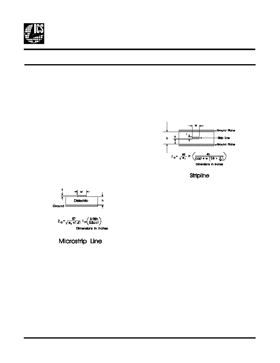
wires. These lines can take two forms: microstrip and stripline.
A microstrip line is shown below:
Essentially, the microstrip is a copper trace on a PCB over a
ground plane. Typically, the dielectric is G10 glass epoxy. It
differs from a standard PCB trace in that its width is calculated
to have a characteristic impedance. To calculate the charac-
teristic impedance of a microstrip line one must know the width
and thickness of the trace, and the thickness and dielectric
constant of the dielectric. For G10 glass epoxy, the dielectric
constant (e
r
) is about 5. Propagation delay is strictly a function
of dielectric constant. For G10 propagation, delay is calculated
to be 1.77 ns/ft.
Stripline is the other form a PCB transmission line can take. A
buried trace between ground planes (or between a power plane
and a ground plane) is common in multi-layer boards.
Attempting to create a workstation design without the use of
multi-layer boards would be adventurous to say the least, the
issue would more likely be whether to place the interconnect
on the surface or between layers. The between layer approach
would work better from an EMI standpoint, but would be more
difficult to lay out. A stripline is shown below:
Using 1oz. copper (0.0015" thick) and 0.040" thickness G10,
a 0.010" trace will exhibit a characteristic impedance of 75
in a stripline configuration.
Typically, RAMDACS require a V
ih
of V
AA
-1.0 Volts as a
guaranteed logical "1" and a V
il
of V
AA
-1.6 as a guaranteed
logical "0." Worst case input capacitance is 10 pF.
Output circuitry for the ICS1572 is shown in the following
diagram. It consists of a 4/1 current mirror, and two open drain
output FETs along with inverting buffers to alternately enable
each current-sinking driver. Both CLK and CLK- outputs are
connected to the respective CLOCK and CLOCK* inputs of
the RAMDAC with transmission lines and terminated in their
equivalent impedances by the Thevenin equivalent impedances
of R1 and R2 or R1' and R2'.
ICS1572 Application Information
Output Circuit Considerations for the ICS1572
17
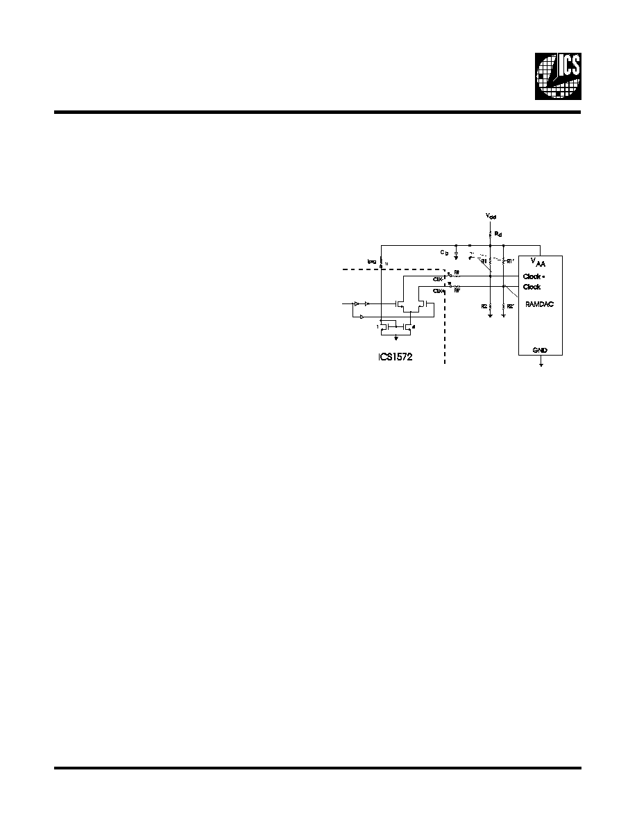
The ICS1572 is incapable of sourcing current, so V
ih
must be
set by the ratios of these resistors for each of these lines. R1
and R2 are electrically in parallel from an AC standpoint
because V
dd
is bypassed to ground through bypass-capacitor
network C
b
. If we picked a target impedance of 75
for our
transmission line impedance, a value of 91
for R1 and R1'
and a value of 430
for R2 and R2' would yield a Thevinin
equivalent characteristic impedance of 75.1W and a Vih value
of VAA-.873 Volts, a margin of 0.127Volts. This may be
adequate; however, at higher frequencies one must contend
with the 10 pF input capacitance of the RAMDAC. Values of
82
for R1 and R1' and 820
for R2 and R2' would give us a
characteristic impedance of 74.5
and a V
ih
value of V
AA
-.45.
With a .55 Volt margin on V
ih
, this voltage level might be safer.
To set a value for V
il
, we must determine a value for I
prg
that
will cause the output FET's to sink an appropriate current. We
desire V
il
to be V
AA
-1.6 or greater. V
AA
-2 would seem to be a
safe value. Setting up a sink current of 25 milliamperes would
guarantee this through our 82
pull-up resistors. As this is
controlled by a 4/1 current mirror, 7 mA into I
prg
should set this
current properly. A 510
resistor from V
dd
to I
prg
should work
fine.
Resistors Rt and Rt' are shown as series terminating resistors
at the ICS1572 end of the transmission lines. These are not
required for operation, but may be useful for meeting EMI
requirements. Their intent is to interact with the input capaci-
tance of the RAMDAC and the distributed capacitance of the
transmission line to soften up rise and fall times and conse-
quently cut some of the high-order harmonic content that is
more likely to radiate RF energy. In actual usage they would
most likely be 10 to 20
resistors or possibly ferrite beads.
C
b
is shown as multiple capacitors. Typically, a 22
�
F tantalum
should be used with separate .1
�
F and 220pf capacitors placed
as close to the pins as possible. This provides low series
inductance capacitors right at the source of high frequency
energy. R
d
is used to isolate the circuitry from external sources
of noise. Five to ten ohms should be adequate.
Great care must be used when evaluating high frequency
circuits to achieve meaningful results. The 10 pf input capaci-
tance and long ground lead of an ordinary scope probe will
make any measurements made with it meaningless. A low
capacitance FET probe with a ground connection directly
connected to the shield at the tip will be required. A 1GHz
bandwidth scope will be barely adequate, try to find a faster
unit.
ICS1572 Application Note
ICS1572 Output Circuitry
18

LEAD COUNT
14L
16L
18L
20L
24L
28L
32L
DIMENSION L
0.354
0.404
0.454
0.504
0.604
0.704
0.804
Ordering Information
ICS1572M-101 or ICS1572M-301
Example:
ICS XXXX M -XXX
Pattern Number (2 or 3 digit number for parts with ROM code patterns)
Package Type
M=SOIC
Device Type (consists of 3 or 4 digit numbers)
Prefix
ICS, AV=Standard Device; GSP=Genlock Device
SOIC Packages (wide body)
ICS1572
19