 | –≠–ª–µ–∫—Ç—Ä–æ–Ω–Ω—ã–π –∫–æ–º–ø–æ–Ω–µ–Ω—Ç: ICS162834 | –°–∫–∞—á–∞—Ç—å:  PDF PDF  ZIP ZIP |

Integrated
Circuit
Systems, Inc.
ICS162834
Advance Information
0774--02/10/03
Recommended Applications:
∑ PC133 Registered Memory Module
∑ PC motherboards
∑ Servers and workstations
∑ Provides complete PC133 DIMM solution with
ICSVF2509, ICSVF2510 PLL.
Product Features:
∑ Meets JESD 82-2 specification
∑ Internal series resistors to reduce switching noise
∑ ±12 mA device capability
∑ Low voltage operation
- V
DD
= 3.3 ± 0.3V
∑ 0.50 mm pitch, 56-Pin TSSOP package
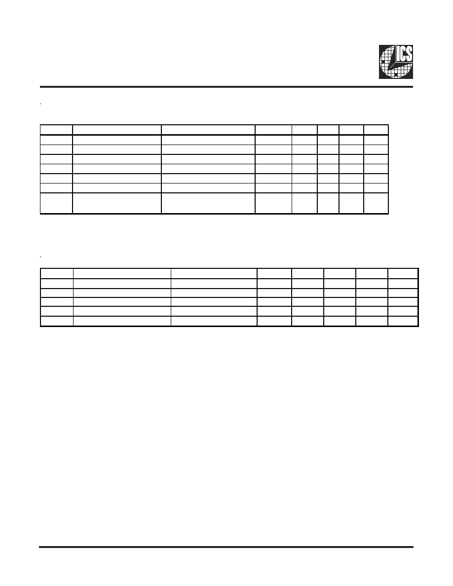
18-Bit 3.3V Registered Buffer
Function Table
1
Block Diagram
Notes:
1.
H = HIGH Voltage Level
L = LOW Voltage Level
X = Don't Care
Z = High-Impedance
= LOW-to-HIGH Transition
2.
Output level before the indicated steady-state
input conditions were established, provided that
CLK is HIGH before LE# went LOW.
3.
Output level before the indicated steady-state
input conditions were established.
s
t
u
p
n
I
s
t
u
p
t
u
O
#
E
O
#
E
L
K
L
C
x
A
x
Y
H
X
X
X
Z
L
L
X
L
L
L
L
X
H
H
L
H
L
L
L
H
H
H
L
H
H
X
Y
0
)
2
(
L
H
L
X
Y
0
)
3
(
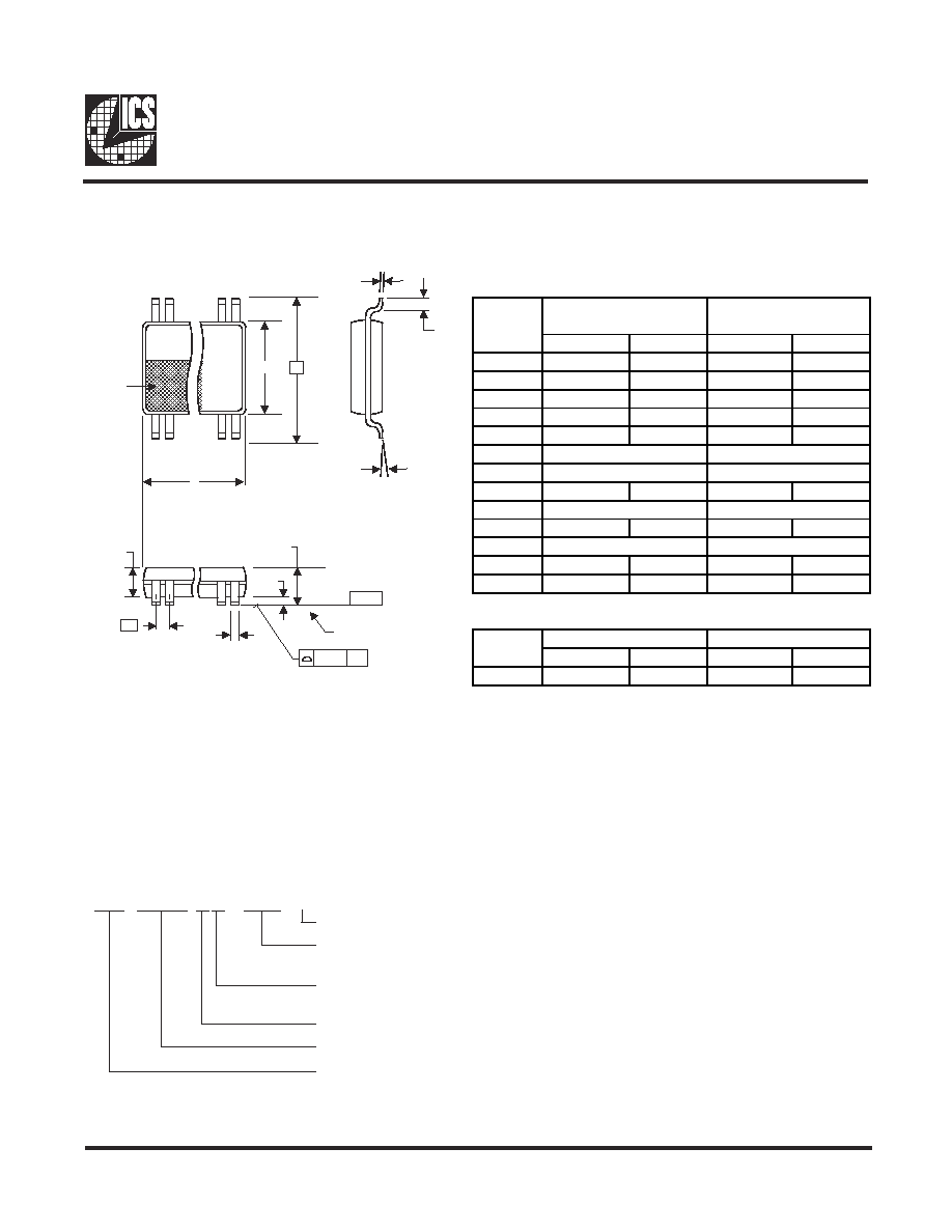
Pin Configurations
56-Pin TSSOP
6.10 mm. Body, 0.50 mm. pitch
ADVANCE INFORMATION documents contain information on products in the formative or design phase development. Characteristic data and other specifications are design goals.
ICS reserves the right to change or discontinue these products without notice. Third party brands and names are the property of their respective owners.
Pin Description
s
e
m
a
N
n
i
P
n
o
i
t
p
i
r
c
s
e
D
#
E
O
)
w
o
L
e
v
i
t
c
A
(
t
u
p
n
I
e
l
b
a
n
E
t
u
p
t
u
O
K
L
C
t
u
p
n
I
k
c
o
l
C
#
E
L
t
u
p
n
I
e
l
b
a
n
E
h
c
t
a
L
x
A
t
u
p
n
I
a
t
a
D
x
Y
s
t
u
p
t
u
O
a
t
a
D
V
D
D
e
g
a
t
l
o
V
y
l
p
p
u
S
D
N
G
d
n
u
o
r
G
1
2
3
4
5
6
7
8
9
10
11
12
13
14
15
16
17
18
19
20
21
22
23
24
25
26
27
28
29
30
31
32
56
55
54
53
52
51
50
49
48
47
46
45
44
43
42
41
40
39
38
37
36
35
34
33
ICS162834
NC
NC
Y1
GND
Y2
Y3
VDD
Y4
Y5
Y6
GND
Y7
Y8
Y9
Y10
Y11
Y12
GND
Y13
Y14
Y15
VDD
Y16
Y17
GND
Y18
OE#
LE#
GND
NC
A1
GND
A2
A3
VDD
A4
A5
A6
GND
A7
A8
A9
A10
A11
A12
GND
A13
A14
A15
VDD
A16
A17
GND
A18
CLK
GND
OE#
CLK
A1
LE#
To 17 Other Channels
C1
1D
CK
Y1

2
ICS162834
Advance Information
0774--02/10/03
General Description
The ICS162834 low voltage 18-bit register combines D-type latches and D-type flip-flops to allow data flow in
transparent, latched and clocked modes. Date flow is controlled by output-enable (OE#), latch enable (LE#),
and clock (CLK) inputs. The device operates in transparent mode when LE# is held low. The device operates
in clocked mode when LE# is high and CLK is toggled. Data transfers from the inputs (A[18:1]) to outputs
(Y[18:1]) on a positive edge transition of the clock. When OE# is low, the output state is enabled. When OE#
is high, the output port is in a high impedance state.
The 18-bit registered buffer is designed to operate with a 3.0V to 4.6V supply voltage.
All inputs support operation with standard LVTTL interface levels. This includes data inputs, clock inputs and
control inputs. Device outputs meet the requirements of the PC133 Registered DIMM specification. The device
functions as defined supports latched, registered and flow through modes of operations. The PC133
Specification requires only registered mode.
Package is a 56 thin shrink small-outline package as defined by JEDEC Publication, JEP95, MO-153.

3
ICS162834
Advance Information
0774--02/10/03
Absolute Maximum Ratings
Storage Temperature . . . . . . . . . . . . . . . . . . . . ≠65∞C to + 150∞C
Supply Voltage (V
DD
) . . . . . . . . . . . . . . . . . . . -0.5 to 4.6V
Input Voltage
(V
I
) . . . . . . . . . . . . . . . . . . . . . . . -0.5 to 4.6V
Output Voltage (V
O
) . . . . . . . . . . . . . . . . . . . . -0.5 to V
DDQ
+ 0.5
Input Clamp Current (I
IK
) . . . . . . . . . . . . . . . . 50 mA
Output Clamp Current (I
OK
) . . . . . . . . . . . . . . ±50 mA
Continuous Output Current (I
O
) . . . . . . . . . . . ±50 mA
V
DD
, V
DDQ
or GND Current/Pin . . . . . . . . . . . ±100 mA
Package Thermal Impedance
,
O
JA . . . . . . . . . . .
64∞C/W
Stresses above those listed under
Absolute Maximum Ratings may cause permanent damage to the device. These
ratings are stress specifications only and functional operation of the device at these or any other conditions above those
listed in the operational sections of the specifications is not implied. Exposure to absolute maximum rating conditions
for extended periods may affect product reliability.
Recommended Operating Conditions
PARAMETER
MIN
TYP
MAX
V
DD
3.0
3.3
3.6
V
IN
-0.3
3.6
0
V
DD
0
V
DD
T
A
0
70
V
OUT
Voltage Applied to
output or I/O pins
Outputs enabled
Outputs high-Z
DESCRIPTION
Supply Voltage
Voltage Applied to input pins
Operating free-air temperature
Switching Characteristics
MIN
MAX
t
PLH
, t
PHL
Propagation Delay CLK to
Yx
1.8
3.5
ns
t
SK(0)
Output Skew*
-
500
ps
f
CLOCK
150
-
MHz
Symbol
V
CC
= 3.3V ± 0.15V
UNITS
Parameter
* Skew between any two putputs of the same package and switching in the
same direction
4
ICS162834
Advance Information
0774--02/10/03
Electrical Characteristics - DC
T
A
= 0 - 70∞ C; V
DD
= 3.3 ± 0.3V, V
DDQ
=3.3 ± 0.3V; (unless otherwise stated)
SYMBOL
PARAMETERS
CONDITIONS
V
DD
(V)
MIN
TYP
MAX
UNITS
V
IH
HIGH-level input voltage
3.0 - 3.6
2.0
V
V
IL
LOW-level input voltage
3.0 - 3.6
0.8
V
V
OH
HIGH-level output voltage
I
OH
= -12 mA, V
IH
= 2.0V
3.0
2.2
V
V
OL
Low-level output voltage
I
OL
= 12 mA, V
IL
= 0.8V
3.0
0.8
I
I
Input leakage current
V
I
= V
DD
or GND
3.0 - 3.6
±10
µA
I
OZ
Off-state leakage current
V
O
= V
DD
or GND#, OE = V
DD
±20
µA
I
DD
Quiescent Supply Current
V
I
= V
DD
or GND, I
O
= 0
±40
µA
* Parameters are characterized over recommended operating conditions.
Critical Register Specifications*
SYMBOL
PARAMETERS
CONDITION
V
DD
(V)
MIN
TYP
MAX
UNITS
t
PD
**
Propagation Delay (CK to Y)
R
L
= 500
, C
L
= 50 pF
3.0 - 3.6
1.4
3.5
ns
t
PD
**
Propagation Delay (CK to Y)
R
L
= 500
, C
L
= 30 pF
3.0 - 3.6
0.7
2.5
ns
t
S
Setup time (A before CK)
3.0 - 3.6
1.0
ns
t
H
Hold time (A after CK)
3.0 - 3.6
0.6
ns
C
I
Clock input capacitance
3.0 - 3.6
3.3
4.0
6.0
pF
* Parameters are characterized over recommended operating conditions.
** The t
PD
value in this table would equate to the 'Time-to-Vm' delay described in the post register timing specifications of the
PC133 registered DIMM Specification. The first value applies to DIMMs with nine SDRAM loads per register output, and the
second to DIMMs with eighteen SDRAM loads per register output. These values should serve as only an initial starting point,

5
ICS162834
Advance Information
0774--02/10/03
d
e
t
s
e
T
r
e
t
e
m
a
r
a
P
n
o
i
t
i
s
o
P
h
c
t
i
w
S
t
H
L
P
n
e
p
O
t
L
H
P
n
e
p
O
t
H
Z
P
D
N
G
t
L
Z
P
V
x
2
D
D
t
Z
H
P
D
N
G
t
Z
L
P
V
x
2
D
D
DUT
RL
CL
RL
2 x VDD
Open
GND
Puls e
Generator
RT
Test circuit component values:
R
L
= Load Resistor = 500
C
L
= Load Capacitance and includes probe and jig capacitance
R
T
= Termination resistance should be equal to Z
OUT
of Pulse Generator
V
IN
= 0 to V
DD
t
r
= t
f
2.0 ns (10% to 90%) unless otherwise specified.
Test Circuit
Test Circuit and Switching Waveforms

6
ICS162834
Advance Information
0774--02/10/03
5
IN PUT
V
IH
0V
V
O H
V
O L
t
PLH1
t
SK
(x)
OU TPUT 1
OU TPUT 2
t
PH L1
t
SK
(x)
t
PLH2
t
PH L2
V
T
V
T
V
O H
V
T
V
O L
t
SK
(x)
= t
PLH2
-
t
P LH1
or
t
PH L2
-
t
P HL1
LOW -H IGH -LOW
PU LSE
H IGH -LOW -H IGH
PU LSE
V
T
t
W
V
T
C ON TR OL
IN PUT
t
PLZ
0V
OU TPU T
N OR M ALLY
LOW
t
PZH
0V
SW ITCH
CLO SE D
OU TPU T
N OR M ALLY
H IGH
EN ABLE
D ISABLE
SW ITCH
OPEN
t
PH Z
0V
V
LZ
V
O H
V
T
V
T
t
PZ L
V
LO AD /2
V
LO AD /2
V
IH
V
T
V
O L
V
HZ
NOTES:
Switching Waveforms
1. For t
SK
(o) OUTPUT1 and OUTPUT2 are any two outputs.
2. For t
SK
(b) OUTPUT1 and OUTPUT2 are in the same bank.
ENABLE AND DISABLE TIMES
OUTPUT SKEW -
t
SK(X)
NOTE:
1. Diagram shown for input Control Enable-LOW and input Control
Disable-HIGH.
PULSE WIDTH
An
CK
Yn
tPLH
tPHL
VIH
VIL
VIH
VIL
VOH
VOL
An
CK
Yn
tS
tS
VIH
VIH
VIL
VIH
VIL
VOH
VOL
An
CK
Yn
tH
tH
VIH
VIL
VIH
VIL
VOH
VOL
HOLD TIME MEASUREMENTS
PROPAGATION DELAY MEASUREMENT
SETUP TIME MEASUREMENTS
7
ICS162834
Advance Information
0774--02/10/03
Ordering Information
ICS162834AG-T
Designation for tape and reel packaging
Pattern Number (2 or 3 digit number for parts with ROM code
patterns)
Package Type
G = TSSOP
Revision Designator (will not correlate with datasheet revision)
Device Type (consists of 3 or 4 digit numbers)
Prefix
ICS, AV = Standard Device
Example:
ICS XXXX y G - PPP - T
INDEX
AREA
INDEX
AREA
1 2
1 2
N
D
E1
E
a
SEATING
PLANE
SEATING
PLANE
A1
A
A2
e
- C -
- C -
b
c
L
aaa
C
6.10 mm. Body, 0.50 mm. pitch TSSOP
(240 mil)
(0.020 mil)
MIN
MAX
MIN
MAX
A
--
1.20
--
.047
A1
0.05
0.15
.002
.006
A2
0.80
1.05
.032
.041
b
0.17
0.27
.007
.011
c
0.09
0.20
.0035
.008
D
E
E1
6.00
6.20
.236
.244
e
L
0.45
0.75
.018
.030
N
0∞
8∞
0∞
8∞
aaa
--
0.10
--
.004
VARIATIONS
MIN
MAX
MIN
MAX
56
13.90
14.10
.547
.555
10-0039
N
D mm.
D (inch)
Reference Doc.: JEDEC Publication 95, M O-153
0.50 BASIC
0.020 BASIC
SEE VARIATIONS
SEE VARIATIONS
SEE VARIATIONS
SEE VARIATIONS
8.10 BASIC
0.319 BASIC
SYMBOL
In Millimeters
In Inches
COMMON DIMENSIONS COMMON DIMENSIONS