
Integrated
Circuit
Systems, Inc.
General Description
Features
ICS1886
Block Diagram
PHYceiver is a trademark of Integrated Circuit Systems, Inc.
FDDI / Fast Ethernet PHYceiver
TM
ICS1886RevC120996
Data and clock recovery for: 32.064 Mb/s (Japan)
34.368 Mb/s (Europe - E3) 125 MHz (Ethernet)
139.264 Mb/s (Europe - E4)
Clock multiplication from either a crystal, differential
or single-ended timing source
Continuous clock in the absence of data
No external PLL components
Lock/Loss status indicator output
Loopback mode for system diagnostics
Selectable loop timing mode
PECL drivers with settable sink current
The ICS1886 is designed to provide high performance clock
recovery and generation for either 32.064 Mb/s, 34.368
Mb/s, 125 Mb/s or 139.264 Mb/s NRZ or NRZI serial data
streams. The ICS1886 is ideally suited for LAN transceiver
applications in either European or Japanese communication
environments.
The ICS1886 also operates at the 100Mbit Ethernet
frequency of 125 MHz. This is ideal for serial Ethernet data
applications where no serial to parallel conversion is
required.
Clock and data recovery is performed on an input serial data
stream or the buffered transmit data depending upon the state
of the loopback input. A continuous clock source will
continue to be present even in the absence of input data. All
internal timing is derived from either a low cost crystal or an
external clock module.
The ICS1886 utilizes advanced CMOS phase-locked loop
technology which combines high performance and low
power at a greatly reduced cost.
Pin Configuration
28-Pin SOIC

2
ICS1886
Pin Descriptions
* Active Low Input.
CS1
CS0
LOOP
INPUT
CLOCK FREQ
MODE
REF FREQ or
CRYSTAL
VSS
VSS
VSS
Tx Data
32.064 MHz
Japan
4.008 MHz
VSS
VDD
VSS
Tx Data
34.368 MHz
Europe - E3
4.296 MHz
VDD
VSS
VSS
Tx Data
125.000 MHz
Ethernet
25.000 MHz
VDD
VDD
VSS
Tx Data
139.264 MHz
Europe - E4
17.408 MHz
VSS
VSS
VDD
Rx Data
32.064 MHz
Japan
4.008 MHz
VSS
VDD
VDD
Rx Data
34.368 MHz
Europe - E3
4.296 MHz
VDD
VSS
VDD
Rx Data
125.000MHz
Ehternet
25.000 MHz
VDD
VDD
VDD
Rx Data
139.264 MHz
Europe - E4
17.408 MHz
Table 1 - Device Clock Selection
PIN
NUMBER
PIN NAME
TYPE
DESCRIPTION
1
VSS
Negative supply voltage.
2
LT~
Loop Timing mode select.*
3
CD~
Carrier Detect input.*
4
TX+
Positive Transmit serial data output.
5
TX-
Negative Transmit serial data output.
6
VSS
Negative supply voltage.
7
IPRG1
PECL Output stage current set (TX).
8
RX-
Negative Receive serial data input.
9
RX+
Positive Receive serial data input.
10
LB~
Loop Back mode select.*
11
LOCK
Lock detect output.
12
CS1
Clock select 1 input.
13
CS0
Clock select 0 input.
14
VSS
Negative supply voltage.
15
IPRG2
PECL Output stage current set (TC, RC and RD).
16
VSS
Negative supply voltage.
17
RD+
Positive recovered data output
18
RD-
Negative recovered data output.
19
RC+
Positive recovered clock output.
20
RC-
Negative recovered clock output.
21
VDD
Positive supply voltage.
22
REF+
Positive reference clock/crystal input.
23
REF-
Negative reference clock/crystal input.
24
VDD
Positive supply voltage.
25
TC-
Negative Transmit clock output.
26
TC+
Positive Transmit clock output.
27
TD-
Negative Transmit data input.
28
TD+
Positive Transmit data input.

3
ICS1886
Absolute Maximum Ratings
V
DD
(measured to V
SS
) . . . . . . . . . . . . . . . . . . 7.0 V
Ambient Operating Temperature . . . . . . . . . . . 55�C to +125�C
Storage Temperature . . . . . . . . . . . . . . . . . . . . 65�C to +150�C
Junction Temperature . . . . . . . . . . . . . . . . . . . 175�C
Soldering Temperature . . . . . . . . . . . . . . . . . . 260�C
Recommended Operating Conditions
Stresses above those listed under Absolute Maximum Ratings above may cause permanent damage to the device. This is a
stress rating only and functional operation of the device at these or any other conditions above those listed in the operational
sections of the specifications is not implied. Exposure to absolute maximum rating conditions for extended periods may
affect product reliability.
ICS1886 FDDI / Fast Ethernet Application
PARAMETER
SYMBOL
TEST CONDITIONS
MIN
MAX
UNITS
Ambient Operating Temp.
T
A
0
+70
�C
Using a Negitive Supply
V
SS
V
DD
-4.50
0.0
-5.50
0.0
V
V
Using a Positive Supply
V
SS
V
DD
0.0
+4.50
0.0
+5.50
V
V

4
ICS1886
V
DD
= V
MIN
to V
MAX
, V
SS
= 0V, T
A
= T
MIN
to T
MAX
Note: REF_IN Input switch point is 50% of VDD.
DC Characteristics
PARAMETER
SYMBOL
CONDITIONS
MIN
MAX
UNITS
Supply Current
I
SS
V
DD
= +5.0V, V
SS
= 0.0V
--
50
mA
ECL Input/Output
PARAMETER
SYMBOL
CONDITIONS
MIN
MAX
UNITS
ECL Input High Voltage
V
I H
V
DD
-1.16
V
DD
-0.88
V
ECL Input Low Voltage
V
I L
V
DD
-1.81
V
DD
-1.47
V
ECL Differential
Threshold Voltage Range
V
T H
--
150
mV
ECL Input Common
Mode Voltage
V
C M
1.3
V
DD
- .4
V
ECL Output High Voltage
V
OH
V
DD
-1.02
--
V
ECL Output Low Voltage
V
OL
--
V
DD
-1.62
V
TTL Input/Output
PARAMETER
SYMBOL
CONDITIONS
MIN
MAX
UNITS
TTL Input High Voltage
V
I H
VDD = 5.0V, VSS = 0.0V
2.0
--
V
TTL Input Low Voltage
V
I L
VDD = 5.0V, VSS = 0.0V
--
0.8
V
TTL Output High Voltage
V
OH
VDD = 5.0V, VSS = 0.0V
2.7
--
V
TTL Output Low Voltage
V
OL
VDD = 5.0V, VSS = 0.0V
--
0.5
V
TTL Driving CMOS
Output High Voltage
V
OH
VDD = 5.0V, VSS = 0.0V
3.68
--
V
TTL Driving CMOS
Output Low Voltage
V
OL
VDD = 5.0V, VSS = 0.0V
--
0.4
V
TTL / CMOS Output
Sink Current
I
OL
VDD = 5.0V, VSS = 0.0V
--
8
mA
TTL / CMOS Output
Source Current
I
OH
VDD = 5.0V, VSS = 0.0V
--
-0.4
mA
REF_IN Input
PARAMETER
SYMBOL
CONDITIONS
MIN
MAX
UNITS
Input High Voltage
V
I H
VDD = 5.0V, VSS = 0.0V
3.5
V
Input Low Voltage
V
I L
VDD = 5.0V, VSS = 0.0V
1.5
V
5
ICS1886
V
DD
= V
MIN
to V
MAX
, V
SS
= 0V, T
A
= T
MIN
to T
MAX
AC Characteristics
PARAMETER
SYMBOL CONDITIONS
MIN
MAX
UNITS
ECL Outputs
Rise/Fall Time
t
r
, t
f
15pF Load
1.4
1.7
ns
Recovered clock
Duty Cycle
t
DC
15pF Load
45
55
%
Output Data Setup
t
sv
W.R.T. RC at 139.264MHz
2.2
3.3
ns
Output Data Hold
t
hd
W.R.T. RC at 139.264MHz
3.9
4.5
ns
Transmit Latency
TL
139.264MHz
6
9
ns
Recieve Latency
RL
139.264MHz
1clock+15
1clock+20
ns
Phase-Locked Loop Characteristics
Lock Acquisition
t
acq
139.264MHz
--
5
�s
Capture Range
139.264MHz
--
�5
% of
center freq.
Receive Jitter Tolerance
t
jt
139.264MHz
--
.15%
UIp-p
Transmit Clock Stability
139.264MHz
17.408MHz crystal
--
6
ppm

6
ICS1886
Input Pin Descriptions
Transmit Data Input (TD+ and TD-) For normal operation
this differential input is transferred to the TX
�
output
through a PECL buffer. In loopback testing mode, this input
is multiplexed to the input of the device clock recovery
section.
Receive Data Input (RX+ and RX-) The clock recovery
and data regenerator from the receive buffer are driven from
this PECL input. During loopback testing mode this input is
ignored.
Clock Select (CS0 and CS1) Selects the operating
frequency according to Table 1. Internal pull-up resistors
set both inputs high when left unconnected.
Carrier Detect (CD~) Active low input which forces the
VCO to free run. Upon receipt of a loss of input signal
(such as from an optical-to-elec-trical transducer), the
internal phase-lock loop will free-run at the selected
operating frequency. Also, when asserted, CD will set the
lock output low.
Loop Timing Mode (LT~) Active low input which routes
the recovered receive clock to the TC
�
outputs as well as
the RC
�
outputs. Forces the transmit clock to be loop-
timed to the system clock derived from the incoming data.
Loopback Mode (LB~) Active low input which causes the
clock recovery PLL to operate using the transmit TD
�
input
data and ignore the receive RX
�
data. Utilized for system
loopback testing.
External Crystal or Reference Clock (REF+ and REF-)
This oscillator input can be driven from either a
fundamental mode crystal or a stable reference. For either
method, the reference frequency is
1
/
8
the operating
frequency. See Table 1 for more information.
Output Pin Descriptions
Transmit Data Differential
ECL (TX+ and TX-) This differential output is buffered TD
�
data. This output remains active during loopback mode.
Transmit Clock Differential ECL (TC+ and TC-)
Differential output clock used by the PDH/ATM processor
for clocking out transmit data. This clock can be derived
from either an independent clock source or from the
recovered data clock (system loop time mode).
Receive Data Differential ECL (RD+ and RD-) The
regenerated differential data derived from the serial data
input. In loopback mode this data is regenerated from the
transmit data input (TD
�
). This data is phase-aligned with
the negative edge of the RC clock output.
Receive Clock Differential ECL (RC+ and RC-) The
differential clock recovered with the internal clock recov-
ery PLL. In loopback mode this clock is recovered from the
transmit data (TD
�
) input. This clock is phase-aligned with
the RD data output.
Lock/Loss Detect (LOCK) Set high when the clock
recovery PLL has locked onto the incoming data. Set low
when there is no incoming data, which in turn causes the
PLL to free-run. This signal can be used to indicate or
alarm the next receive stage that the incoming serial data
has stopped.
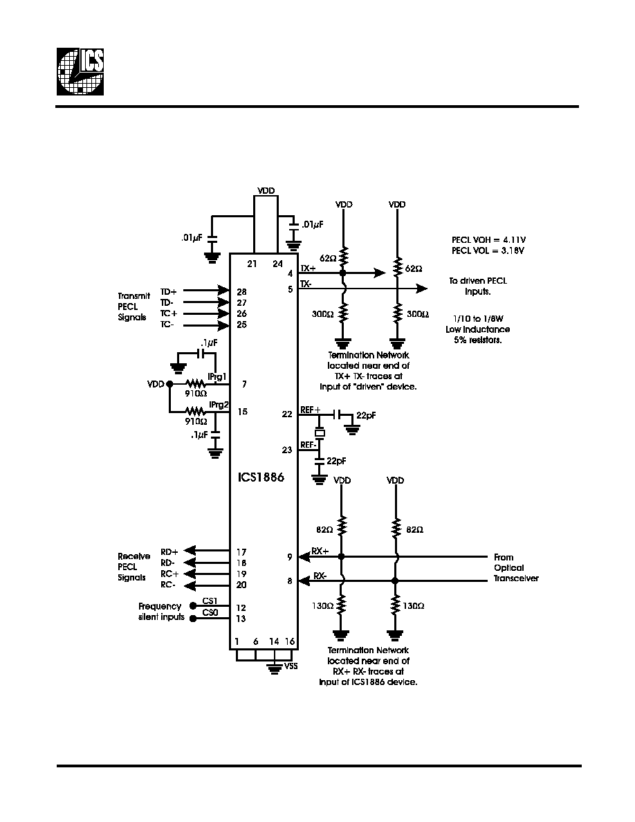
Output Description
The differential output drivers are current mode and are de-
signed to drive resistive terminations in a complementary
fash-ion. The outputs are current-sinking only, with the
amount of sink current programmable via the IPRGx pins.
The sink current is equal to four times the IPRGx current.
For most applications, a resistor from VDD to IPRGx will
set the current to the necessary precision. IPRG1 supplies
the current mirror for the TX
�
output. IPRG2 supplies the
current mirrors for the RD
�
, RC
�
and TC
�
outputs.
The differential PECL output pins are incapble of sourcing
current, so V
OH
must be set by the ratios of the termination
resistors for each of these lines. R1 is a pull-up resistor
con-nected from the PECL output to VSS. R1 and R2 are
electrically in parallel from an AC stand point. If we pick a
target imped-ance of 50
for our transmission line
impedance, a value of 62
for R1 and a value of 300
for
R2 would yield a Thevenin equivalent characteristic
impedance of 50
and a V
OH
value of V
DD
-.88 volts,
compatible with PECL circuits.
To set a value for V
OL
, we must determine a value for Iprg
that will cause the output FETs to sink an appropriate
current. We desire V
OL
to be V
DD
-1.81 or greater. Setting
up a sink current of 19 milliamperes would guarantee this
through out output terminating resistors. As this is
controlled by a 4/1 current mirror, 4.75mA into Iprg should
set this current properly. An 910
resistor from V
DD
to
Iprg should work fine.
7
ICS1886
ICS1886 PECL Termination for 50W Transmission Lines
8
ICS1886
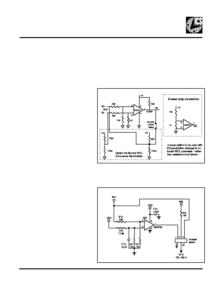
The current ICS1886 device provides a single
TTL-compatible input, carrier detect (CD~).
When carrier detect is asserted, the ICS1886
locks to the incoming receive data. When
carrier detect is deasserted, or if carrier detect
is asserted and no data is present on the receive
inputs, the PLL will free run and continue to
provide RXCLK at the nominal 25 MHz
frequency. This provides a continuous Receive
clock source, even if CD~ is always tied to
ground.
If a true signal detect is required by a chip that
connects to the ICS1886, a simple, low cost
PECL to CMOS converter can be used. The
following circuits implement this function:
These circuits provide PECL to CMOS
conversion for less than $0.80 in single unit
quantities. Note that the LM393 has two
amplifiers, so the unused one is tied inactive.
A running production change will be made to
the ICS1886 to change the CD~ input to PECL.
Therefore, boards should be layed out with a
direct normal PECL termination connection
stuffing option. This allows either version of
the part to be used by stuffing one of two sets
of external components. A version of this
circuit is shown in the diagram above.
Option 2
Single-Ended PECL to CMOS Conversion Circuit
Option 1
Differential PECL to CMOS Conversion Circuit
CD PECL Input: Board Layout Options

9
ICS1886

10
ICS1886
Ordering Information
ICS1886M
SOIC PACKAGE
ICS XXXX M
Package Type
M = SOIC
Device Type (consists of 3 or 4 digit numbers)
Prefix
ICS, AV = Standard Device
Example:
LEAD COUNT
2 8L
DIMENSION L
0.704