 | –≠–ª–µ–∫—Ç—Ä–æ–Ω–Ω—ã–π –∫–æ–º–ø–æ–Ω–µ–Ω—Ç: ICS1887M | –°–∫–∞—á–∞—Ç—å:  PDF PDF  ZIP ZIP |
Integrated
Circuit
Systems, Inc.
General Description
Features
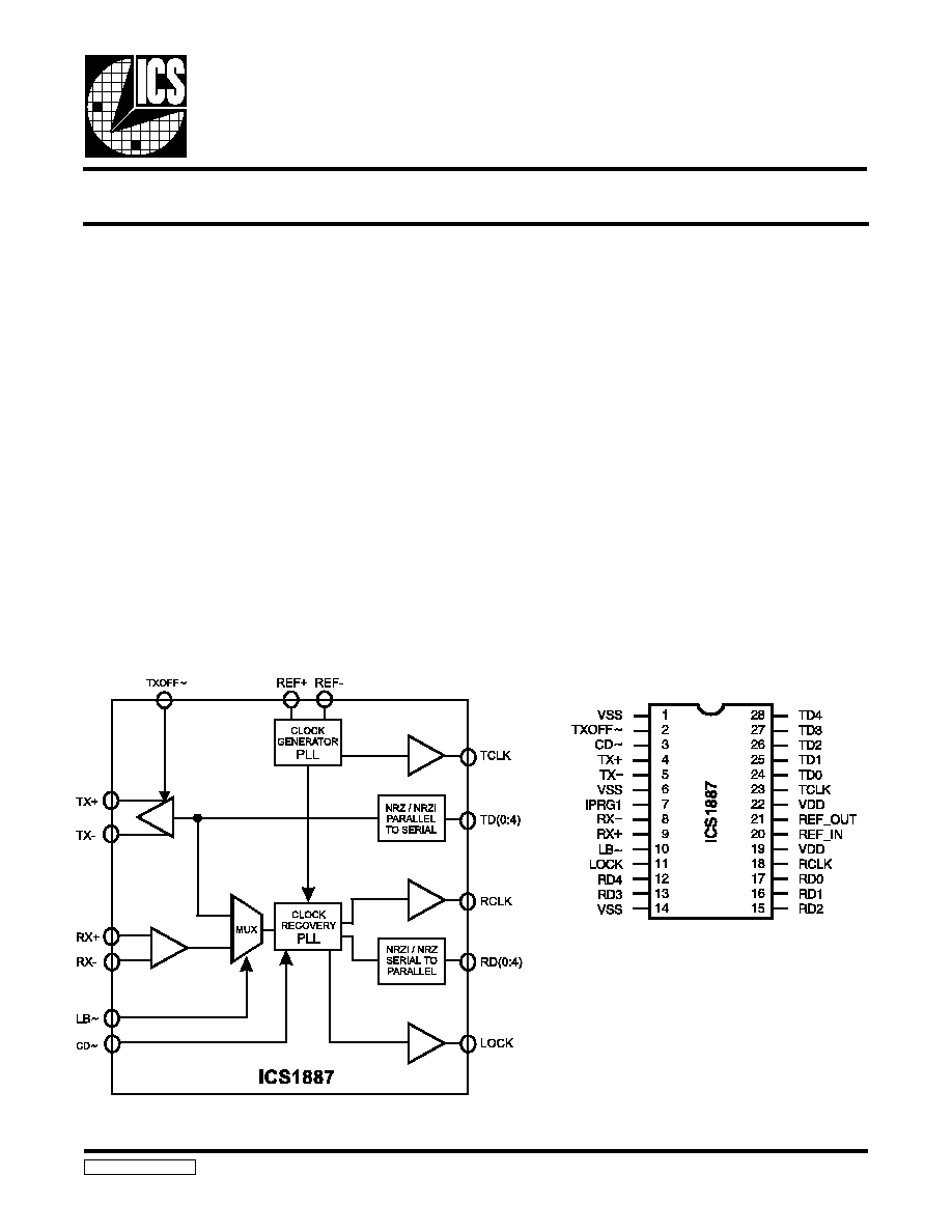
ICS1887
Block Diagram
PHYceiver is a trademark of Integrated Circuit Systems, Inc.
FDDI / Fast Ethernet PHYceiver
TM
ICS1887RevF112596
∑
Single IC solution to existing designs requiring
multiple devices
∑
Data and clock recovery for 125 MBaud FDDI or Fast
Ethernet applications
∑
Clock multiplication from either a crystal, differential
or single-ended timing source
∑
Continuous clock in the absence of data
∑
No external PLL components
∑
Lock/Loss status indicator output
∑
Loopback mode for system diagnostics
∑
Selectable loop timing mode
∑
PECL driver with settable sink current
∑
Parallel digital transmit and receive data interface
∑
NRZ to/from NRZI data conversion
∑
Consult ICS for optional configurations and data rates
The ICS1887 is designed to provide high performance clock
recovery and generation for 125 MHz serial data streams. The
ICS1887 is ideally suited for LAN transceiver applications in
either FDDI or Fast Ethernet environments. The ICS1887
converts NRZ to/from NRZI data in addition to providing a
5-bit parallel digital data transmit and receive interface.
Clock and data recovery is performed on an input serial data
stream or the buffered transmit data depending upon the state
of the loopback input. A continuous clock source will
continue to be present even in the absence of input data.
All internal timing is derived from either a low cost crystal,
differential or single-ended source.
The ICS1887 utilizes advanced CMOS phase-locked loop
technology which combines high performance and low power
at a greatly reduced cost.
Pin Configuration
28-Pin SOIC
2
ICS1887
Pin Descriptions
Note:
1. A running production change will be made to this input in the June 1996 time frame to convert this
input from the TTL-compatible to PECL to more closely match applications requirements. See
Substituting the ICS1887 for the AMD PDR & PDT applications note for more information.
2. This pin was formerly used for Loop-Timed operation. If your design did not use loop timing, this
change does not affect you. If your application requires loop timing, please contact ICS.
* Active Low Input.
PIN
NUMBER
PIN NAME
TYPE
DESCRIPTION
1
VSS
Negative Supply Voltage
2
TXOFF~
2
TTL-Compatible
Transmitter Off*
3
CD~
TTL-Compatible
1
Carrier Detect input*
4
TX+
PECL
Positive Transmit serial data output
5
TX≠
PECL
Negative Transmit serial data output
6
VSS
Negative supply voltage
7
IPRG1
PECL Output stage current set (TX)
8
RX≠
PECL
Negative Receive serial data input
9
RX+
PECL
Positive Receive serial data input
10
LB~
TTL-Compatible
Loop Back mode select*
11
LOCK
TTL-Compatible
Lock detect output
12
RD4
TTL-Compatible
Recovered data output 4
13
RD3
TTL-Compatible
Recovered data output 3
14
VSS
Negative supply voltage
15
RD2
TTL-Compatible
Recovered data output 2
16
RD1
TTL-Compatible
Recovered data output 1
17
RD0
TTL-Compatible
Recovered data output 0
18
RCLK
TTL-Compatible
Recovered Receive clock output
19
VDD
Positive supply voltage
20
REF_IN
Positive reference clock/crystal input
21
REF_OUT
Negative reference clock/crystal output
22
VDD
Positive supply voltage
23
TCLK
TTL-Compatible
Transmit clock output
24
TD0
TTL-Compatible
Transmit data input 0
25
TD1
TTL-Compatible
Transmit data input 1
26
TD2
TTL-Compatible
Transmit data input 2
27
TD3
TTL-Compatible
Transmit data input 3
28
TD4
TTL-Compatible
Transmit data input 4

3
ICS1887
Input Pin Descriptions
Parallel Transmit Data (TD0 .. TD4)
Five bit TTL compatible digital input, which is received by
the ICS1887 on the positive edge of TCLK. High impedance
input drivers routed to the serial NRZ to NRZI converter. In
loopback testing mode, this NRZI data is multiplexed to the
input of the device clock recovery section.
Differential ECL Receive Data Input (RX+ & RX-)
The clock recovery and data regenerator from the receive
buffer are driven from this PECL input. During loopback test-
ing mode this input is ignored.
Carrier Detect (CD~)
Active low input which forces the VCO to free run. Upon
receipt of a loss of input signal (such as from an optical-to-
electrical transducer), the internal phase-lock loop will
free-run at the selected operating frequency. Also, when
asserted, CD will set the lock output low.
Transmitter Off (TXOFF~)
Active low input which, when low, forces TX+ low and
TX-high. When high, data passes through TX+ and TX-
unaffected. This input has an internal pull-up resistor.
Loopback Mode (LB~)
Active low input which causes the clock recovery PLL to
operate using the transmit input data reference and ignore the
receive RX
±
data. Utilized for system loopback testing.
External Crystal or Reference Clock
(REF_IN and REF_OUT)
This oscillator input can be driven from either a fundamental
mode crystal or a stable reference. For either method, the ref-
erence frequency is 25.00 MHz.
Output Pin Descriptions
Differential ECL Transmit Data (TX+ and TX-)
This differential output is converted TD[0..4] serial data. This
output remains active during loopback mode.
Transmit Clock (TCLK)
TTL compatible 25 MHz clock used by the parallel processor
transmitter for clocking out transmit data. This clock can be
derived from either an independent clock source or from the
recovered data clock (system loop time mode).
Parallel Receive Data (RD0 .. RD4)
The regenerated five bit parallel data derived from the serial
data input. In loopback mode this data is regenerated from the
transmit data. This data is phase-aligned with the negative
edge of RCLK clock output.
Receive Clock (RCLK)
A 25 MHz digital clock recovered with the internal clock
recovery PLL. In loopback mode this clock is recovered from
the transmit data.
Lock/Loss Detect (LOCK)
Set high when the clock recovery PLL has locked onto the
incoming data. Set low when there is no incoming data, which
in turn causes the PLL to free-run. This signal can be used to
indicate or `alarm' the next receive stage that the incoming
serial data has stopped.
Output Description
The differential driver for the TX
±
is current mode and is de-
signed to drive resistive terminations in a complementary
fashion. The output is current-sinking only, with the amount
of sink current programmable via the IPRG1 pin. The sink
current is equal to four times the IPRG1 current. For most
applications, an 910
resistor from VDD to IPRG1 will set
the current to the necessary precision.
The TX
±
pins are incapable of sourcing current, so V
OH
must
be set by the ratios of the Thevenin termination resistors for
each of these lines. R1 is a pull-up resistor connected from the
PECL output to VDD. R2 is a pull-down resistor connected
from the PECL output to VSS. R1 and R2 are electrically in
parallel from an AC standpoint. If we pick a target impedance
of 50
for our transmission line impedance, a value of 62
for R1 and a value of 300
for R2 would yield a Thevinin
equivalent characteristic impedance of 50
and a V
OH
value
of V
DD
-.88 volts, compatible with PECL circuits.
To set a value for V
OL
, we must determine a value for I
prg
that
will cause the output FET's to sink an appropriate current. We
desire V
OL
to be V
DD
-1.81 or greater. Setting up a sink current
of 19 milliamperes would guarantee this through our output
terminating resistors. As this is controlled by a 4/1 current
mirror, 4.75 mA into I
prg
should set this current properly. An
910
resistor from V
DD
to I
prg
should work fine.

4
ICS1887
ICS1887 System Diagram
(PECL Termination for 50
Transmission Lines)
5
ICS1887
This note describes the issues involved in re-
placing the AMD PDR & PDT with the
ICS1887.
There are a number of implementation differ-
ences between AMD's PDR & PDT and the
ICS1887. This note describes the differences
and how they affect an application.
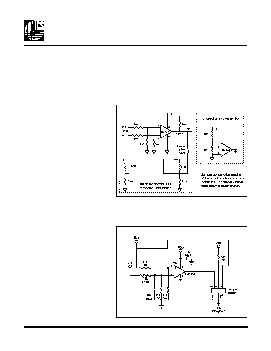
Signal Detect
Many twisted pair and fiber optic transceivers
provide a signal detect indication that becomes
active when the amount of energy being re-
ceived reaches a threshold that makes it appear
to be data and not ambient noise.
The AMD PDR device has a single ended
PECL input (SDI) and provides a TTL level
output (SDO) that tracks the input. The input
controls the source that the PLL locks to. When
signal detect is asserted, the PLL locks to the
incoming receive data. When signal detect is
deasserted, the PLL locks to the LSCLK input
to prevent locking to an off center frequency.
The current ICS1887 device provides a single
TTL-compatible input, carrier detect (CD~).
When carrier detect is asserted, the ICS1887
locks to the incoming receive data. When car-
rier detect is deasserted, or if carrier detect is
asserted and no data is present on the receive
inputs, the PLL will free run and continue to
provide RXCLK at the nominal 25 MHz
frequency. This allows the carrier detect input
to always be tied to an asserted level (ground).
If a true signal detect is required by a chip that
connects to the ICS1887, a simple, low cost
PECL to CMOS converter can be used. The
following circuit implements this function:
Substituting the ICS1887
for the AMD PDR & PDT
Option 2
Single-Ended PECL to CMOS Conversion Circuit
CD PECL Input: Board Layout Options
Option 1
Differential PECL to CMOS Conversion Circuit

6
ICS1887
This circuit provides the PECL to CMOS conversion for less
than $0.80 in single unit quantities. Note that the LM393 has
two amplifiers, so the unused one is tied inactive.
A running production change will be made to the ICS1887 to
change the CD input to PECL. Therefore, boards should be
laid out with a direct normal PECL termination connection
stuffing option. This allows either version of the part to be
used by stuffing one of two sets of external components. A
version of this circuit is shown in the diagram on the previous
page.
With ICS1887 devices that have a TTL-compatible CD input,
the "Differential PECL to CMOS Conversion Circuit" com-
ponents need to be placed on the PCB and the "Normal PECL
Transceiver Termination" resistors (82
and 130
) as well as
the option select jumper should NOT be placed.
When the final ICS1887 device with the PECL CD input is
used, none of the components in the "Differential PECL to
CMOS Conversion Circuit" or the "Unused amp connection"
circuits should be used. Only the four termination resistors
(87
and 130
) and the option select jumper are needed.
Note that these resistors should be located near the ends of the
transmission lines.
Clocking
Parallel data that is to be serialized for transmission must be
presented to the data transmitter device with a certain amount
of setup and hold time to a given clock.
The PDT chip expects data to setup relative to the 25 MHz
Local Symbol Clock (LSCLK). This clock is an input to the
device.
The ICS1887 expects data to be setup relative to the 25 MHz
Reference In Clock (REF_IN). This clock is an input to the
ICS1887 device. Note that the REF_IN pin of the ICS1887 is
a CMOS input with a switching point of 50% of VDD. If this
pin is driven by a TTL output, a pull-up resistor to VDD must
be used. The ICS1887 device also provides a Transmit Clock
(TXC) output, which is a 50% duty cycle (nominal) copy of
the REF_IN input. The ICS1887 is designed to provide a very
low skew between the REF_IN and the TCLK.
Loopback
The AMD PDR & PDT chips have an external loopback con-
nection between the two chips. The ICS1887 also has a
loopback function, but it is totally internal to the device.
Optical Transmitter Off Control
The PDT chip has an input (FOTOFF) which can force an
optical transceiver to be off. The ICS1887 performs the same
behavior with the TXOFF~ pin.
Test Mode
Both the AMD PDR & PDT have a test mode that allows auto-
mated testers to test internal logic without the PLL clock
multiplier. The ICS1887 does not have a similar test mode.
Transmit Current Selection
The ICS1887 allows the PECL transmit current level to be set
externally. An 887
resistor to the VDD supply is recom-
mended.
7
ICS1887
Absolute Maximum Ratings
V
DD
(measured to V
SS
) . . . . . . . . . . . . . . . . . . 7.0 V
Digital Inputs/Outputs . . . . . . . . . . . . . . . . . . V
SS
≠ 0.5 V to V
DD
+ 0.5 V
Ambient Operating Temperature . . . . . . . . . . ≠ 55∞ C to +125∞C
Storage Temperature . . . . . . . . . . . . . . . . . . . . ≠ 65∞ C to +150∞ C
Junction Temperature . . . . . . . . . . . . . . . . . . . 175∞C
Soldering Temperature . . . . . . . . . . . . . . . . . . 260∞ C
Recommended Operating Conditions
Stresses above those listed under Absolute Maximum Ratings above may cause permanent damage to the device. This is a stress
rating only and functional operation of the device at these or any other conditions above those listed in the operational sections
of the specifications is not implied. Exposure to absolute maximum rating conditions for extended periods may affect product
reliability.
PARAMETER
SYMBOL
TEST CONDITIONS
MIN
MAX
UNITS
Ambient Operating Temp.
T
A
0
+70
∫C
Using a Positive Supply
V
SS
V
DD
0.0
+4.50
0.0
+5.50
V
V
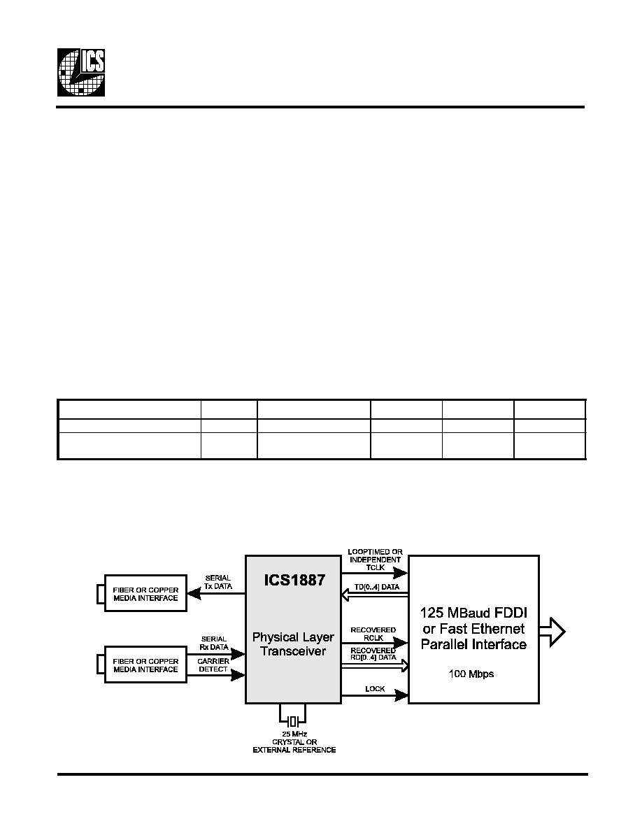
ICS1887 FDDI / Fast Ethernet Application
8
ICS1887
PARAMETER
SYMBOL
CONDITIONS
MIN
MAX
UNITS
Supply Current
I
DD
V
DD
= +5.0V, V
SS
= 0.0V
--
80
mA
PARAMETER
SYMBOL
CONDITIONS
MIN
MAX
UNITS
ECL Input High Voltage
V
I H
V
DD
-1.16
V
DD
-0.88
V
ECL Input Low Voltage
V
I L
V
DD
-1.81
V
DD
-1.47
V
ECL Differential
Threshold Voltage Range
V
T H
--
150
mV
ECL Input Common
Mode Voltage
V
C M
1.3
V
DD
- .4
V
ECL Output High Voltage
V
O H
V
DD
-1.02
--
V
ECL Output Low Voltage
V
O L
--
V
DD
-1.62
V
PARAMETER
SYMBOL
CONDITIONS
MIN
MAX
UNITS
TTL Input High Voltage
V
I H
VDD = 5.0V, VSS = 0.0V
2.0
--
V
TTL Input Low Voltage
V
I L
VDD = 5.0V, VSS = 0.0V
--
0.8
V
TTL Output High Voltage
V
O H
VDD = 5.0V, VSS = 0.0V
2.4
--
V
TTL Output Low Voltage
V
O L
VDD = 5.0V, VSS = 0.0V
--
0.4
V
TTL Driving CMOS
Output High Voltage
V
O H
VDD = 5.0V, VSS = 0.0V
3.68
--
V
TTL Driving CMOS
Output Low Voltage
V
O L
VDD = 5.0V, VSS = 0.0V
--
0.4
V
TTL / CMOS Output
Sink Current
I
O L
VDD = 5.0V, VSS = 0.0V
8
--
mA
TTL / CMOS Output
Source Current
I
O H
VDD = 5.0V, VSS = 0.0V
--
-0.4
mA
PARAMETER
SYMBOL
CONDITIONS
MIN
MAX
UNITS
Input High Voltage
V
I H
VDD = 5.0V, VSS = 0.0V
3.5
--
V
Input Low Voltage
V
I L
VDD = 5.0V, VSS = 0.0V
--
1.5
V
V
DD
= V
MIN
to V
MAX
, V
SS
= 0V, T
A
= T
MI N
to T
MAX
Note: REF_IN Input switch point is 50% of VDD.
ECL Input / Output
TTL Input / Output
REF_IN Input
DC Characteristics

9
ICS1887
AC Characteristics
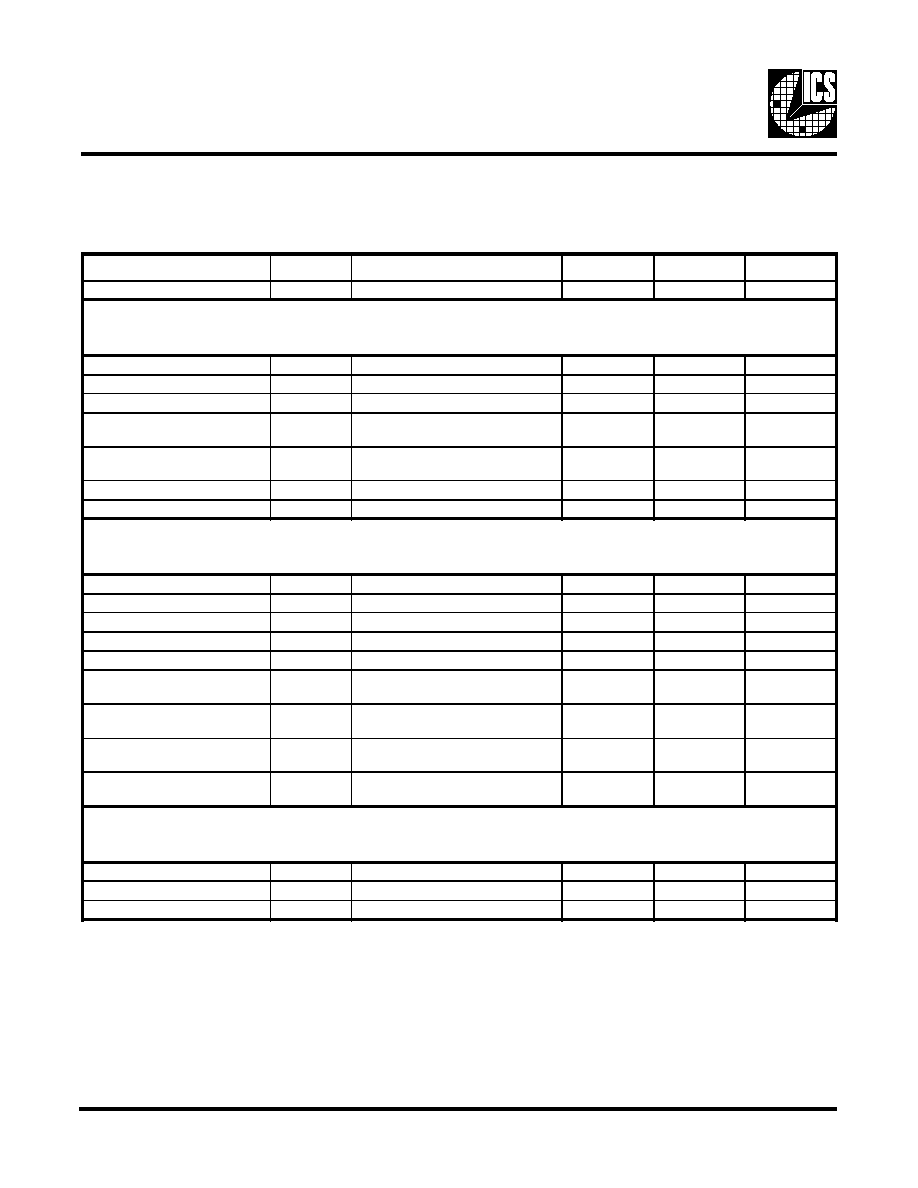
Clocks ≠ Reference In (REF_IN) to Transmit Clock (TCLK)
T#
PARAMETER (conditions)
MIN
TYP
MAX
UNITS
t1
REF_IN Duty Cycle
45
50
55
%
t2
REF_IN Period
--
40
--
ns
t3
REF_IN rise to TCLK rise
0
1.5
3.0
ns
10
ICS1887
Clocks -- Transmit Clock Tolerance
Clocks -- Receive Clock Tolerance
Note: TCLK Duty cycle = REF_IN Duty cycle ±5%.
T#
PARAMETER (conditions)
MIN
TYP
MAX
UNITS
t1
TCLK Duty Cycle
40
50
60
%
t2
TCLK Period
--
40
--
ns
T#
PARAMETER (conditions)
MIN
TYP
MAX
UNITS
t1
RCLK Duty Cycle
45
50
55
%
t2
RCLK Period
--
40
--
ns

11
ICS1887
5-Bit Interface ≠ Synchronous Transmit Timing
5-Bit Interface ≠ Synchronous Receive Timing
T#
PARAMETER (conditions)
MIN
TYP
MAX
UNITS
t1
TD[4:0] Setup to TCLK rise
10
--
--
ns
t2
TD[4:0] Hold after TCLK rise
0
--
--
ns
T#
PARAMETER (conditions)
MIN
TYP
MAX
UNITS
t1
RD[4:0] Setup to RCLK rise
13.0
--
--
ns
t2
RD[4:0] Hold after RCLK rise
12.5
--
--
ns

12
ICS1887
Transmit Latency
Receive Latency
T#
PARAMETER (conditions)
MIN
TYP
MAX
UNITS
t1
TD[4:0] sampled to TX+ Output of 1st bit
--
--
5
bits
T#
PARAMETER (conditions)
MIN
TYP
MAX
UNITS
t1
MSbit into RX+ to MSb on RD[4:0]
--
--
8
bits
13
ICS1887
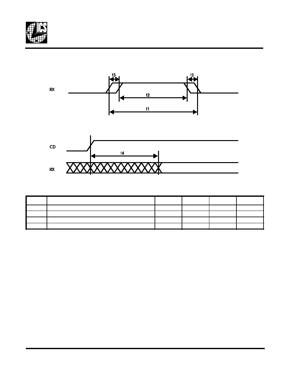
Clock Recovery
T#
PARAMETER (conditions)
MIN
TYP
MAX
UNITS
t1
Ideal data recovery window
--
--
8
ns
t2
Actual data recovery window
6
--
8
ns
t3
Data recovery window truncation
0
--
1
ns
t4
CD assert to data acquired
--
--
5
µ s

14
ICS1887
Ordering Information
ICS1887M
SOIC PACKAGE
ICS XXXX M
Package Type
M = SOIC
Device Type (consists of 3 or 4 digit numbers)
Prefix
ICS, AV = Standard Device
Example:
LEAD COUNT
2 8 L
DIMENSION L
0.704