Integrated
Circuit
Systems, Inc.
General Description
Features
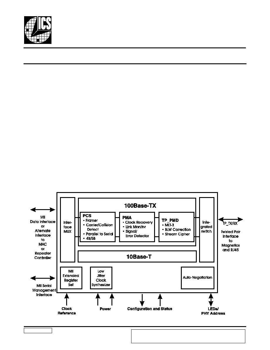
ICS1890
10Base-T/100Base-TX Integrated PHYceiver
ICS1890RevG 10/21/97
Block Diagram
One chip integrated physical layer
All CMOS, Low power design (<200mA max)
Small footprint 64-pin 14mm
2
QFP package
ISO/IEC 8802-3 CSMA/CD compliant
Media Independent Interface (MII)
Alternate 100M stream and 10M 7-wire serial
interfaces provided
10Base-TX Half & Full Duplex
100Base-TX Half & Full Duplex
Fully integrated TP-PMD including Stream
Cipher Scrambler, MLT-3 encoder, Adaptive
Equalization, and Baseline Wander Correction
Circuitry
PHYceiver and QuickPoll are trademarks of Integrated
Circuit Systems, Inc. Patents pending.
The ICS1890 is a fully integrated physical layer device
supporting 10 and 100Mb/s CSMA/CD Ethernet applications.
DTE (adapter cards or motherboards), switching hub, repeater
and router applications are fully supported. The ICS1890
is compliant with the ISO/IEC 8802-3 Ethernet standard
for 10 and 100Mb/s operation. A Media Independent Interface
allowing direct chip-to-chip connection, motherboard-to-
daughterboard connection or connection via an AUI-like
cable is provided. A station management interface is
provided to enable command information and status
information exchange. The ICS1890 interfaces directly to
transmit and receive isolation transformers and can support
shielded twisted pair (STP) and unshielded twisted pair
(UTP) category 5 cables up to 105 meters. Operation in half
duplex or full duplex modes at either 10 or 100 Mbps
speeds is possible with control by Auto-Negotiation or
manual selection. By employing Auto-Negotiation the
technology capabilities of the remote link partner may be
determined and operation automatically adjusted to the
highest performance common operating mode.
ICS reserves the right to make changes in the device data identified in this publication
without further notice. ICS advises its customers to obtain the latest version of all
device data to verify that any information being relied upon by the customer is current
and accurate.

2
ICS1890
Introduction
The ICS1890 is essentially a nibble/bit stream processor.
When transmitting, it takes sequential nibbles presented at
the Media Independent Interface (MII) and translates them to
a serial bit stream for transmission on the media. When receiving,
it takes the serial bit stream from the media and translates it to
sequential nibbles for presentation to the MII. It has no
knowledge of the underlying structure of the MAC frame it is
conveying.
100Base-TX Operation
When transmitting, the ICS1890 encapsulates the MAC
frame (including the preamble) with the start-of-stream and
end-of-stream delimiters. When receiving, it strips off the
SSD and substitutes the normal preamble pattern and then
presents this and subsequent preamble nibbles to the MII.
When it encounters the ESD, it ends the presentation of
nibbles to the MII. Thus, the MAC reconciliation layer sees
an exact copy of the transmitted frame.
During periods when no frames are being transmitted or
received, the device signals and detects the idle condition.
This allows the higher levels to determine the integrity of the
connection. In the 100Base-TX mode, a continuous stream of
scrambled ones is transmitted signifying the idle condition.
The receive channel includes logic that monitors the IDLE
data stream to look for this pattern and thereby establishes
the link integrity.
The 100M Stream Interface option allows access to raw groups
of 5-bit data with lower latency through the PHY. This is useful
in building repeaters where latency is critical.
10Base-T Operation
In 10Base-T mode, the bit stream on the cable is identical to
the de-composed MAC frame. Link pulses are used to establish
the channel integrity. When receiving, the ICS1890 first
synchronizes to the preamble. Once lock is detected, it begins
to present preamble nibbles to the MII. On detection of the
SFD, it frames the subsequent 4-bits which are the first data
nibble.
Configuration
The ICS1890 is designed to be fully configurable using
either hardware pins or the (usually) software-driven MII
Management interface, as selected with the HW/SW pin. A
rich set of configuration options are provided. This allows
diverse system implementations and costs.

3
ICS1890
Modes of Operation
Reset & Basic Initialization
Reset can be accomplished using either register bit 0:15 or the
RESET pin.
For a hardware reset, RESET must be held at a logic zero level
for at least two clock cycles and may be held low as long as
desired.
While RESET is held low the device is in Low Power mode.
After the RESET pin is released to a logic one level, Low
Power mode is exited, the PHY address is latched into register
16, and the reset process continues to completion.
For a software reset, a management agent must write a logic
one to register bit 0:15. This will start the reset process. The
software reset bit will clear itself automatically when reset is
completed.
All reset timing parameters are specified in the Electricals
section of the data sheet.
Low Power and Automatic 100Base-T Power-
Down
The ICS1890 supports two power saving modes. The ICS1890
device can be placed into a state where very littler power is
drawn by the device. This Low Power mode can be activated
by holding the RESET pin continuously low or by writing a
logic one to the Power-down bit (0:11).
When the device is in Low Power mode, all functions are
disabled except for register access through the MII Management
Interface.
All register values are maintained during Low Power mode,
except for latching status bits, which are reset to their default
values.
The ICS1890 can also automatically reduce its total power
requirements when operating in 10Base-T mode by automatically
powering-down the 100Base-TX modules.
The power required by the ICS1890 in normal, 100Base-TX
power-down, and Low Power modes is given in the Electricals
section of the data sheet.
Auto-Negotiation
A link can automatically be established using Auto-Negotiation.
When enabled, Auto-Negotiation will exchange information
about the local nodes capabilities with its remote link partner.
After the information is exchanged, each device compares its
capabilities with those of its partner and then the highest
performance operational mode is automatically selected.
As an example, if one device supports 10Base-T and 100Base-
TX, and the other device supports 100Base-TX and 100Base-
T4, 100Base-TX will automatically be selected.
See the Auto-Negotiation section for more details on how the
process is initiated and controlled.
100Base-TX
The primary operational mode of the ICS1890 is to provide
100Base-TX physical layer services. This consists mainly of
converting data from parallel to serial at a 100 Mb/s data rate.
The device may be configured in a number of different ways
and also provides detailed operational status information.
10Base-T
The ICS1890 also provides 10Base-T physical layer services
to allow easy migration from 10 to 100 Mb/s service. Complete
data service is provided with configuration and status available
to management.
Full Duplex
The ICS1890 supports either half and full duplex operation
for both 10Base-T and 100Base-TX. Full Duplex operation
allows simultaneous transmission and reception of data which
can effectively double data throughput to 20 or 200 Mb/s.
To operate in Full Duplex mode, some of the standard 10Base-
T and 100Base-TX behaviors are modified.
In 10Base-T Full Duplex mode, transmitted data is not looped
back to the receiver and SQE test is not performed.
In both 10Base-T and 100Base-TX Full Duplex modes, CRS is
asserted in response only to receive activity and COL always
remains inactive.

4
ICS1890
Interface Overviews
Overview of MAC/Repeater to PHY Interfaces
To accommodate different applications, the ICS1890 provides
four types of MAC/Repeater to PHY interfaces. The four
interfaces are - 10/100 MII Data Interface, 100M Stream Inter-
face, 10M Serial Interface and the Link Pulse Interface.
The standard and most commonly used interface is the 10/100
MII Data Interface which provides framed 4-bit nibbles and
control signals.
The 100M Stream Interface provides 5-bits of unframed data
as well as the normal CRS signal which can be used as a fast
look-ahead. This interface is intended for 100Base-TX repeater
applications that require nothing more than recovered parallel
data where all framing is handled in the repeater core logic.
The 10M Serial Interface provides a framed single data bit
interface with control signals and is ideally suited to applications
that already incorporate a serial 10Base-T MAC with a standard
7-wire interface.
The Link Pulse Interface is provided for applications that wish
to fully control the Auto-Negotiation process themselves but
not the actual generation and reception of Link Pulses.
MII Data Interface
The ICS1890 implements a fully compliant IEEE 802.3u
Media Independent Interface for connection to MACs or
repeaters allowing connection between the ICS1890 and
MAC on the same board, motherboard/daughter board or via
a cable in a similar manner to AUI connections.
The MII is a specification of signals and protocols which
formalizes the interfacing of a 10/100 Mbps Ethernet Media
Access Controller (MAC) to the underlying physical layer.
The specification is such that different physical media may be
supported (such as 100Base-TX, 100Base-T4 and 100Base-
FX) transparently to the MAC.
The MII Data Interface specifies transmit and receive data
paths. Each path is 4-bits wide allowing for transmission of a
data nibble. The transmit data path includes a transmit clock
for synchronous transfer, a transmit enable signal and a transmit
error signal. The receive data path includes a receive data
clock for synchronous transfer, a receive data valid signal and
a receive error signal. Both the transmit clock and receive
clock are sourced by the ICS1890.
The ICS1890 provides the MII signals carrier sense and
collision detect. In half duplex mode, carrier sense indicates
that data is being transmitted or received, and in full duplex
mode it indicates that data is being received. Collision detect
indicates that data has been received while a transmission is
in progress.

5
ICS1890
The ICS1890 is designed to allow hot insertion of an MII
cable into a MAC MII port. During the power-up phase, the
ICS1890 will isolate the MII and the Twisted Pair Transmit
signal pair
100M Stream Interface
The 100M Stream Interface is an alternative parallel interface
between the PHY and MAC/Repeater than the standard MII
Data interface. The Stream Interface provides a lower level
interface and, therefore, lower bit delay than the standard MII
Data Interface.
This interface is selected by setting the MII/SI pin to STREAM
INTERFACE mode and by setting the 10/100SEL pin to 100
mode.
The Stream Interface bypasses the Physical Coding Sublayer
(PCS) and provides a direct unscrambled, unframed 5-bit
interface to the Physical Media Access (PMA) layer.
The Stream Interface consists of a 14 signal interface: STCLK,
STD[4:0], SRCLK, SRD[4:0], SCRS, SD.
Data is exchanged between the MAC and PHY using 5-bit
unframed code groups at 25 MHz clock rate.
The Stream Interface provides a CRS signal by continuing to
use the logic that is bypassed by this interface. This gives a
carrier indication faster than is possible from the MAC/Repeater
since the bits are examined serially as soon as they enter the
PHY.
Since only the Stream Interface or the MII Interface is active
at once, it is possible to share the MII Data interface pins for
Stream Interface functionality.
The pins have the following mapping:
MII
Stream
TXCLK
STCLK
TXEN
(1)
TXER
STD4
TXD3
STD3
TXD2
STD2
TXD1
STD1
TXD0
STD0
RXCLK
SRCLK
RXDV
(2)
RXER
SRD4
RXD3
SRD3
RXD2
SRD2
RXD1
SRD1
RXD0
SRD0
CRS
SCRS
COL
(3)
LSTA
SD
(1) 100Base-TX is a continuous transmission system and the
MAC/Repeater is responsible for sourcing IDLE symbols
when it is not transmitting data when using the Stream Interface.
(2) Since data is not framed when this interface is used, RXDV
has no meaning.
(3) Since the MAC/Repeater is responsible for sourcing both
active and idle data, the PHY can not tell when it is transmitting
in the traditional sense, so no collisions can be detected.
Other mode configuration pins behave identically regardless
of which data interface is used.

6
ICS1890
10M Serial Interface
The 10M Serial Interface is an alternative serial interface
between the PHY and MAC/Repeater than the standard MII
Data interface. The 10M Serial interface provides the same
functionality, but with a serial data stream at a 10 MHz clock
rate.
This interface is selected by setting the MII/SI pin to STREAM
INTERFACE mode and by setting the 10/100SEL pin to 10
mode.
The 10M Serial Interface operation consists of a nine signal
interface: 10TCLK, 10TXEN, 10TD 10RCLK, 10RXDV, 10RD,
10CRS, 10COL, and LSTA.
Data is exchanged between the MAC and PHY serially at a 10
MHz clock rate.
Since only the 10M Serial Interface or the MII Interface is
active at once, it is possible to share the MII Data interface
pins for 10M Serial Interface functionality.
The pins have the following mapping:
MII
10M Serial
TXCLK
10TCLK
TXEN
10TXEN
TXER
(1)
TXD3
TXD2
TXD1
TXD0
10TD
RXCLK
10RCLK
RXDV
10RXDV
RXER
(1)
RXD3
RXD2
RXD1
RXD0
10RD
CRS
10CRS
COL
10COL
LSTA
LSTA
(1) Error generation and detection is not supported by
10Base-T.
Other mode configuration pins behave identically regardless
of which data interface is used.
Link Pulse Interface
The Link Pulse Interface is an alternative control interface
between the PHY and MAC/Repeater than the standard MII
Data interface. The Link Pulse provides detailed control over
the Auto-Negotiation process.
This interface is selected by setting the MII/SI pin to STREAM
INTERFACE mode, by setting the 10/100SEL pin to 10
mode, and by setting the 10/LP pin to LP mode.
The Link Pulse Interface consists of a five signal interface:
LTCLK, LPTX, LRCLK, LPRX, SD.
Since only the Link Pulse Interface or the MII Interface is
active at once, it is possible to share the MII Data interface
pins for Link Pulse Interface functionality.
The pins have the following mapping:
MII
Link Pulse
TXCLK
LTCLK
TXEN
TXER
LPTX
TXD3
TXD2
TXD1
TXD0
RXCLK
LRCLK
RXDV
RXER
LPRX
RXD3
RXD2
RXD1
RXD0
CRS
COL
LSTA
SD
Other mode configuration pins behave identically
regardless of which data interface is used.

7
ICS1890
MII Management Interface
The MII also specifies a two-wire management interface and a
protocol between station management and the physical layer.
The ICS1890 implements this interface, providing a
bidirectional data line and a clock input for synchronizing the
data transfers. This interface allows station management to
read from and write to all of the devices registers.
Twisted Pair Interface
The ICS1890 is able to operate in either 10Base-T or 100Base-
TX modes using a shared interface to a universal magnetics
module and single RJ-45 connector jack.
The interface signals consist of a differential pair of transmit
signals and a differential pair of receive signals. The interface
also provides pins for setting the 10 & 100M transmit current.
Clock Reference Interface
The ICS1890 synthesizes all its required clock signals from
a single 25MHz frequency reference supplied to the Clock
Reference Interface (REF_IN & REF_OUT).
Any reference must meet the stringent IEEE standard
requirements for total accuracy under all conditions of ±50
parts per million (ppm), even though the device can easily
function with a less accurate reference.
Three reference configurations are supported.
A simple CMOS level signal may be fed into the REF_IN
input, leaving the REF-output unconnected.
A crystal oscillator module may be used to provide the
frequency reference for the REF_IN input instead of simple
reference.
It is possible to use a high precision crystal between the
REF_IN and REF_OUT pins on the ICS1890 to provide the
25MHz time base for part operation. In addition to the
connection of the crystal between these pins, a capacitor
from REF_IN and REF_OUT to ground is necessary to
neutralize the capacitance of the crystal. Since these capacitors
are nominally in series, the values of each of these components
(plus stray board capacitance) will equal twice the rated
capacitance of the crystal (series combination).
It is imperative that the crystal be cut for accuracy and
temperature coeffieients with the equivalent capacitive loading
of the specific board layout and the chosen neutralizing
capacitors. The overall accuracy for ethernet applications
must be ±50ppm total for accuracy, temperature, and aging.
Therefore the crystal must be cut using a fixture with the
equivalent capacitive loading as in the end application. This
custom cutting of the crystal will be at additional cost, but
in high volume applications this may be cost effective compared
to pretuned crystal oscillator modules. For more information,
contact ICS Datacom Applications.
Configuration and Status Interface
This interface provides a full set of pins to allow the device
to be completely configured by hardware.
The interface also provides dynamic tristate control over
both the Twisted Pair Transmit interface and the MII Receive
interface.
Link Status and Stream Cipher Locking status signals are
provided for use by a MAC or custom logic.
PHY Address & LED Interface
The ICS1890 device uses a unique scheme to multiplex the
PHY Address and the LED outputs onto the same set of five
pins.
Simply connecting the LED from the device pin to either
power or ground sets the address bit to a 1 or 0. The device
then uses the address info to drive the LED correctly
independent of its connection. The Pin Description section
provides detailed connection instructions.

8
ICS1890
Functional Blocks
Media Independent Interface (MII) Overview
The MII consists of a data interface, basic register set, and a
serial management interface to the register set.
The data interface is a nibble wide transmit and receive data
interface between the MAC and PHY devices. The interface
supports data transfers at 25 MHz for 100Base-T and 2.5 MHz
for 10Base-T.
The register set consists of basic and extended standard
registers as well as vendor specific registers. There are two
basic registers, a control register to handle basic device
configuration, and a status register to report basic device
abilities and status. The standard extended registers provide
access to an Organizationally Unique Identifier and Auto-
Negotiation functionality.
The ICS1890 also provides vendor specific registers that
enhance the device operation. Among these is the QuickPoll
Detailed Status register which provides a comprehensive set
of real-time device information with only single register access.
Auto-Negotiation
The auto-negotiation logic of the ICS1890 has three main
purposes. Firstly, to determine the capabilities of the remote
partner (device at the other end of the cable). Secondly, to
advertise its own capabilities to the remote partner. And thirdly,
to establish a connection with the remote partner using the
highest performance common connection technology.
The ICS1890 auto-negotiation logic is designed to operate
with legacy 10Base-T networks or newer systems with multiple
connection technology options. When operating with a legacy
10Base-T remote partner, the ICS1890 will select the 10Base-
T operating mode transparently to the remote partner thus
allowing the preservation of existing legacy network structures
without management intervention.
Auto-negotiation is accomplished using a physical signaling
scheme that is transparent at the packet and higher level
protocols. This scheme builds upon the 10Base-T link test
pulse sequence by using a burst of pulses to signal
configuration information between the two devices.
The Fast Link Pulse Bursts are simultaneously exchanged by
both nodes on a link segment the local node encodes the data
from the Auto-negotiation Advertisement Register (register
4) into the FLP Bursts it transmits. The data received from the
link partners FLP Bursts is placed into the Auto-Negotiation
Link Partner Ability Register (register 5). When Auto-Negotiation
is complete (1:5=1 or 17:4=1), the highest priority technology
from the following table that is common in the two registers is
automatically selected as the operating mode.
Priority Resolution Table
Highest Priority Listed first.
1)
100Base-TX Full Duplex
2)
100Base-T4
3)
100Base-TX
4)
10Base-T Full Duplex
5)
10Base-T

9
ICS1890
In the event that the link partner does not support auto-
negotiation, backward compatibility is guaranteed because
legacy systems will not respond to the burst (called Fast Link
Pulses). 10Base-T systems will continue to send 10Base-T
link test pulses which will be interpreted by the ICS1890 as
a 10Base-T technology only device. 100Base-TX systems
would send scrambled idle symbols, which would be interpreted
by the ICS1890 as a 100Base-TX only device. Auto-negotiation
is invoked at power-up, upon request by management, or
manually.
Auto-Negotiation Progress Monitor
Under normal circumstances, Auto-Negotiation is able to
effortlessly establish a connection with the link partner. There
are, however, some situations that may prevent Auto-
Negotiation from completing properly. The Auto-Negotiation
Progress Monitor is designed to provide detailed information
to a station management entity to assist it in making a connection
in the event that Auto-Negotiation is unable to establish a
connection by itself.
During normal Auto-Negotiation operation, the device ex-
changes capability information with its link partner and then
sets the Auto-Negotiation Complete bit in the Status register
(1:5) (also available in the QuickPoll register as bit 17:4) to a
logic one to indicate that the information exchange has completed
successfully and that Auto-Negotiation has handed off the
link startup process to the negotiated technology.
Auto-Negotiation can also accommodate legacy 10Base-T
and 100Base-TX link partners that do not have Auto-Negotiation
capability. In this case, Auto-Negotiation identifies the link
partner as not being Auto-Negotiation able by setting the
LP_AutoNeg_Able bit (6:0) to a logic zero, identifies the
legacy connection to be made by setting the single bit
corresponding to that technology in the AN Link Partner
Abilities Register (either bit 5:7 or 5:5), and finally indicates
Auto-Negotiation Complete.
The entire process, in either case, usually takes less than half
a second to complete. Typically, management will poll the
Auto-Negotiation Complete bit and then the Link Status bit to
determine when a connection has been successfully made
and then the actual type of connection can be determined by
management. This information is all contained in the QuickPoll
register.
When Auto-Negotiation fails, Auto-Negotiation Complete may
never become true or Link Status may never become good.
Station management can detect this condition and discover
why there is a failure to connect by using the detailed information
provided by the Auto-Negotiation Progress Monitor.
The Auto-Negotiation Progress Monitor provides four bits of
status in the QuickPoll Detailed Status register when combined
with the already present Auto-Negotiation Complete bit.
As progress is made through the Auto-Negotiation Arbitration
state machine, higher status values are locked in to the progress
monitor. The status value only is allowed to increase until
either Auto-Negotiation is completed successfully or the
progress monitor status is read by management.
After the status is read by management, the status is reset to
the current status of the Arbitration state machine. After
negotiation has completed successfully, any link failure will
cause the process to being anew.
This behavior allows management to always determine the
greatest forward progress made by the Auto-Negotiation logic.
Status
Progress Monitor Status Bits
A-N Complete
Bit 2
Bit 1
Bit 0
Idle
0
0
0
0
Parallel Detected
0
0
0
1
Parallel Detection Failure
0
0
1
0
Ability Matched
0
0
1
1
Acknowledge Match Failure
0
1
0
0
Acknowledge Matched
0
1
0
1
Consistency Match Failure
0
1
1
0
Consistency Matched
0
1
1
1
Auto-Negotiation Completed Successfully
1
1
1
1

10
ICS1890
100Base-TX Physical Coding Sublayer [PCS]
Carrier Detector & Framer
The carrier detector examines the serial bit stream looking for
the SSD, the JK symbol pair. In the idle state, IDLE symbols
(all logic ones) will be received. If the carrier detector detects a
logic zero in the bit stream, it examines the following bits
looking for the first two non-contiguous zeros, confirms that
the first 5-bits form the J symbol (11000) and asserts carrier
detect. At this point the serial data is framed and the second
symbol is checked to confirm the K symbol (10001). If
successful, the following framed data (symbols) are presented
to the 4B5B decoder. If the JK pair is not confirmed, the false
carrier detect is asserted and the idle state is re-entered.
Collision Detector
Collision is asserted in half-duplex
mode when transmission and data reception occur
simultaneously. In full duplex mode, collision is never asserted.
Parallel/Serial Converter
This block converts data between 5-bit symbols and 1-bit
serial data.
4B/5B Encoder/Decoder
When the ICS1890 is operating in the 100Base-TX mode,
4B5B coding is used. This coding scheme maps a 4-bit nibble
to a 5-bit code group. Since this gives 32 possible symbols
and the data only requires 16 symbols, 16 symbols are designated
control or invalid. The control symbols used are JK as the
start-of-stream delimiter (SSD), TR as the end-of-stream
delimiter (ESD), I as the IDLE symbol and H to signal an
error. All other symbols are invalid and, if detected, will set the
receive error bit in the status register.
When transmitting, nibbles from the MII are converted to 5-
bit code groups. The first 16 nibbles obtained from the MII are
the MAC frame preamble. The ICS1890 replaces the first two
nibbles with the start-of-stream delimiter (the JK symbol
pair). Following the last nibble, the ICS1890 adds the end-of-
stream delimiter (the TR symbol pair).
When receiving, 5-bit code groups are converted to nibbles
and presented to the MII. If the ICS1890 detects one or more
invalid symbols, it sets the receive error bit in the status
register. When receiving a frame, the first two 5-bit code
groups received are the start-of-stream delimiter (the JK
symbol pair), the ICS1890 strips them and substitutes two
nibbles of the normal preamble pattern. The last two 5-bit code
groups are the end-of- stream delimiter (the TR symbol
group), these are stripped from the nibbles presented to the
MAC.
11
ICS1890
Symbol
Meaning
4B Code
3210
5B Code
43210
0
Data 0
0000
11110
1
Data 1
0001
01001
2
Data 2
0010
10100
3
Data 3
0011
10101
4
Data 4
0100
01010
5
Data 5
0101
01011
6
Data 6
0110
01110
7
Data 7
0111
01111
I
Idle
undefined
11111
J
SSD
0101
11000
K
SSD
0101
10001
T
ESD
undefined
01101
R
ESD
undefined
00111
H
Error
undefined
00100
V
Invalid
undefined
00000
V
Invalid
undefined
00001
4B5B Encoding (including invalid test mode coding)
Symbol
Meaning
4B Code
3210
5B Code
43210
8
Data 8
1000
10010
9
Data 9
1001
10011
A
Data A
1010
10110
B
Data B
1011
10111
C
Data C
1100
11010
D
Data D
1101
11011
E
Data E
1110
11100
F
Data F
1111
11101
V
Invalid
undefined
00010
V
Invalid
undefined
00011
V
Invalid
undefined
00101
V
Invalid
undefined
00110
V
Invalid
undefined
01000
V
Invalid
undefined
01100
V
Invalid
undefined
10000
V(S)
Invalid
undefined
11001
Invalid Error Code Test (TXER asserted)
V
Invalid
0 0 1 0
0 0 0 1 0
V
Invalid
0 0 1 1
0 0 0 1 1
V
Invalid
0 1 0 1
0 0 1 0 1
V
Invalid
0 1 1 0
0 0 1 1 0
V
Invalid
1 0 0 0
0 1 0 0 0
V
Invalid
1 0 1 0
0 1 1 0 0
V
Invalid
1 1 0 0
1 0 0 0 0
V(S)
Invalid
1 1 0 1
1 1 0 0 1
I
Idle
1 1 1 1
1 1 1 1 1
J
SSD
1 1 1 0
1 1 0 0 0
K
SSD
1 0 1 1
1 0 0 0 1
T
ESD
1 0 0 1
0 1 1 0 1
R
ESD
0 1 1 1
0 0 1 1 1
H
Error
0 1 0 0
0 0 1 0 0
V
Invalid
0 0 0 0
0 0 0 0 0
V
Invalid
0 0 0 1
0 0 0 0 1

12
ICS1890
100Base-T Physical Media Access [PMA]
Clock Recovery
The Clock Recovery block locks onto the incoming data stream,
extracts the embedded clock, and presents the data synchronized
to the recovered clock. This process produces signals with
very low timing uncertainty and noise (jitter).
In the event that the PLL is unable to lock on to the receive
signal, it generates a not locked signal. The transmit clock
synthesizer provides a center frequency reference for operation
of the clock recovery circuit in the absence of data. The
receive signal detected and not locked signals are both
used by the logic which monitors the receive channel for
errors.
Transmit Clock Synthesizer
The ICS1890 synthesizes the transmit clock using a PLL to
produce 2.5 MHz for 10Base-T and 25 MHz for 100Base-TX.
Internal clock frequencies of 20 MHz and 125 MHz are also
generated. This allows the use of a low cost 25 MHz crystal
oscillator for a low jitter reference frequency.
Signal Detector
The ICS1890 Signal Detector is part of the clock recovery
PLL. It detects a Receive Signal Error if no receive signal is
received and detects a PLL Lock Error if the PLL is unable to
lock on to the receive channel signal. A receive channel error
is defined as the loss of receive signal or the loss of PLL lock.
Remote Fault Signaling
Remote fault signaling allows a
link partner to signal receive channel errors on its transmit
channel. It is then possible to establish the integrity of both
the transmit and receive channels. If auto-negotiation is enabled,
the ICS1890 monitors the receive channel for Fast Link
Pulses or Normal Link Pulses. If an error is detected, the
remote error condition is signaled.
The ICS1890 is able to report a remote fault detected by its
link partner. When the link partner is an ICS1890, a remote
fault will be signaled when it detects a receive signal error. The
definition of a remote fault for a non-ICS1890 link partner is
undefined, but generally will mean that there is a problem with
the integrity of the link partners receive channel.

13
ICS1890
Figure 2
0.1
1
10
100
0
2
4
Resistance (Ohm/m) v. Freq. (MHz)
100Base-T Twisted Pair Physical Media
Dependent [TP-PMD]
Stream Cipher Scrambler/Descrambler
When the ICS1890 is operating in the 100Base-TX mode, a
stream cipher scrambler/descrambler that conforms to the ANSI
Standard X3T9.5 FDDI TP-PMD is employed. The purpose of
the stream cipher scrambler is to randomize the 100 Mbps data
on transmission resulting in a reduction of the peak amplitudes
in the frequency spectrum. The stream cipher descrambler
restores the received 5-bit code groups to their unscrambled
values. The stream cipher scrambler/descrambler is bypassed
in the 100M stream interface mode.
MLT-3 Encoder/Decoder
When the ICS1890 is operating in the 100Base-TX mode, an
MLT-3 encoder and decoder is employed. The encoder converts
the NRZI transmitted bit stream to a three-level code resulting
in a reduction in the energy over the critical frequency range
of 20MHz to 100MHz.The MLT-3 decoder converts the received
three-level code back to an NRZI bit stream.
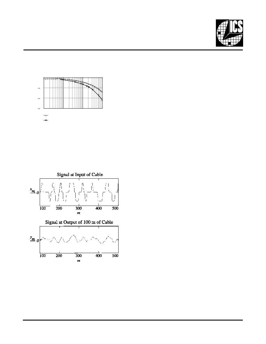
DC Restoration
The 100Base-TX specification uses a stream cipher scrambler
to minimize peak amplitudes in the frequency spectrum.
However, the nature of the stream cipher and MLT-3 encoding
is such that long run lengths of zeroes and ones can cause the
production of a DC component. This DC component cannot
be transmitted through the isolation transformers and results
in baseline wander. Baseline wander decreases noise immunity
since the base-line moves closer to either the positive or
negative signal comparaters. Figure 1 is an exaggerated
simulation of the effect of baseline wander (the time period
would normally be much longer).
The ICS1890 uses DC restoration to restore the lost DC
component of the recovered digital data thus correcting for
baseline wander.
Adaptive Equalizer
The ICS1890 includes an adaptive equalizer to compensate
for signal amplitude and phase distortion incurred from the
transmission media. Signal equalization will actively occur for
twisted pair cable lengths of up to 105 meters.
At a data rate of 100 Mbps, the cable introduces significant
signal distortion due to high frequency roll off and phase
shift. The high frequency loss is mainly due to skin-effect
which causes the conductor resistance to rise as the square of
the frequency (see Figure 2).
Figure 1
14
ICS1890
0.1
1
10
100
30
20
10
0
typical
worst case
Cable Attenuation (dB) v. Freq. (MHz)
Figure 3
Figure 4
Typical and worst case frequency response for 100 meters
(worst case length as derived from draft standard EIA/TIA-
568- A) of UTP Category 5 cable is shown in Figure 3.
The pulse shape of the received signal is critical for MLT-3
encoded data since there are three distinct levels to resolve in
order to properly recover the data. Figure 4 shows the typical
signal at the input and output ends of 100 meters of UTP
Category 5 cable.
Since the cable length that must be equalized can be anything
from 0 to 105 meters, the optimum equalization cannot be fixed,
but must depend on cable length. Thus, adaptive equalization
must be applied at the receive end to restore the signal.
The adaptive equalization process consists of applying increasing
amounts of phase and gain correction while monitoring the
integrity of the recovered data. The adaptive equalizer picks
the best of 32 equalization settings and Fixes this value into
the equalization register. This setting provides the best recovery
of the transmitted data with lowest Bit Error Rate (BER).
Line Transmitter
The line transmitter logic of the ICS1890
is a current-driven differential driver which can be programmed
for either two-level (10Base-T, Manchester) or three-level
(100Base-TX, MLT-3) transmission. Waveshaping is applied
to control the output edge rate and eliminate the need for
expensive external filters. The transmitter interfaces directly to
an inexpensive isolation transformer (magnetics).
Line Receiver
The line receiver circuit accepts either a
differential two-level (10Base-T, Manchester) or three-level
(100Base-TX, MLT-3) signal which first passes through an
isolation transformer. If the polarity correct bit in the Configuration
Register is asserted, the ICS1890 has sensed the reversed
polarity of the receive pair and can switch polarity automatically.
Magnetics
A Universal Magnetics module is used to provide
isolation and signal coupling onto the twisted pair cabling for
both 10Base-T and 100Base-TX.

15
ICS1890
10Base-T Block Diagram
10Base-T
Manchester Encoder/Decoder
When the ICS1890 is operating in the 10Base-T mode,
Manchester coding is used. When transmitting, nibbles from
the MII are converted to a serial bit stream and then Manchester
en-coded. When receiving, the Manchester encoded bit stream
is decoded and converted to nibbles for presentation to the
MII.
Clock Synthesis
A 2.5 MHz clock is synthesized for nibble wide transactions.
A 10 MHz clock is synthesized for serial transactions.
Clock Recovery
The PLL synchronizes on the MAC frame preamble and then
begins recovering data normally.
Idle Function
The Idle function is used to keep a 10Base-T link alive in the
absence of data transmission.
If no data traffic is transmitted for 16ms, a link pulse will be
transmitted. Link pulse transmission will continue every 16ms
until real data is transmitted.
Link Monitor
This function is used to qualify a 10Base-T link. If neither data
or a Link Pulse is received for 50 to 150ms, then the link is
considered down. This state is exited after data is received or
3 to 10 Link Pulses are received.

16
ICS1890
Carrier Detector
In half duplex mode carrier is asserted during transmission or
reception of data. In full duplex or repeater mode, carrier is
asserted only on reception of data.
Collision Detector
Collision occurs whenever there is simultaneous transmit
and receive activity when a half duplex link is established.
Collision never occurs in full duplex mode.
Jabber
The Jabber function prevents the transmitter from erroneously
transmitting for too long a period. The maximum time the
device should transmit continuously is the time it takes to
send a maximum length packet (1500 bytes). The Jabber
function ensures that transmission lasts no longer than 20-
150ms. The typical value for the ICS1890 is 21ms.
When the jabber timer is exceeded, Collision (COL) is
asserted and the transmit output goes idle for 0.5 ±0.25s.
This function can be disabled with the Jabber Inhibit register
bit (18:5).
SQE Test
This test is only used in Half Duplex DTE applications and is
disabled in repeater and Full Duplex mode. This test can also
be disabled with the SQE Test Inhibit register bit (18:2).
When enabled and a link is established, 0.6 to 1.6us after the
last positive transition of a transmitted packet, COL will be
asserted for 10 ±5 bit times.
Manchester Encoder/Decoder
When the ICS1890 is operating in the 10Base-T mode,
Manchester coding is used. When transmitting nibbles from
the MII are converted to a serial bit stream and then Manchester
en-coded. When receiving, the Manchester encoded bit stream
is decoded and converted to nibbles for presentation to the
MH.
Clock Synthesis
A 2.5MHz clock is synthesized for nibble wide transactions.
A 10MHz clock is synthesized for serial transactions.
Clock Recovery
The PLL synchronizes on the MAC fram preamble and then
begins recovering data normally.
Squelch
The squelch function qualifies the data coming into the device
so that spurious noise events are rejected.
Auto Polarity Correction
By examining the polarity of received Link Pulses the ICS1890
can determine if the two wires in the receive data pair were
wired correctly. If the wires were accidentally reversed during
installation, the Auto Polarity Correction function can
automatically correct this in the ICS1890. If the ICS1890
corrects the polarity, this is reflected in the 10Base-T Operations
register. This function can also be disabled through the same
register, if desired.
Line Transmitter
The line transmitter logic of the ICS1890 is a current-driven
differential driver which can be programmed for either two-
level (10Base-T, Manchester) or three-level (100Base-TX, MLT-
3) transmission. Wavespaping is applied to control the output
edge late and eliminate the need for expensive external filters.
The transmitter interfaces directly to an inexpensive isolation
transformer (magnetics).
Line Receiver
The line receiver circuit accepts either a differential two-level
(10Base-T, Manchester) or three-level (100Base-TX, MLT-3)
signal which first passes through an isolation transformer. If
the polarity correct bit in the Configuration Register is asserted,
the ICS1890 will sense the polarity of the receive pair and, if
necessary, switch polarity automatically.
Magnetics
A Universal Magnetics module is used to provide isolation
and signal coupling onto the twisted pair cabling for both
10Base-T and 100Base-TX.

17
ICS1890
Management Interface
The ICS1890 provides a management interface to connect to
a management entity. The two wire serial interface is part of
the MII and is described in the MII section. The interface
allows the transport of status information from the ICS1890
to the management entity and the transport of control information
to the ICS1890. It includes a register set, a frame format, and
a protocol.
Management Register Set
The register set includes the mandatory basic control and
status registers and an extended set. The ICS1890 implements
the following registers.
Control
(register 0)
Status
(register 1)
PHY Identifier
(register 2)
PHY Identifier
(register 3)
Auto-Negotiation Advertisement
(register 4)
Auto-Negotiation Link Partner Ability
(register 5)
Auto-Negotiation Expansion
(register 6)
Reserved by IEEE
(registers 7-15)
Extended Control
(register 16)
QuickPoll Status
(register 17)
10Base-T Operations
(register 18)
Extended Control 2
(register 19)
Reserved by ICS
(registers 20-31)
Management Frame Structure
The management interface uses a serial bit stream with a
specified frame structure and protocol as defined below.
Preamble
11...11
(32 ones)
SOF
01
(2 bits)
Op Code
10 (read), 01 (write)
(2 bits)
Address
AAAAA
(5 bits)
Register
RRRRR
(5 bits)
TA
NN
(2 bits)
Data
DD...DD
(16 bits)
Idle
Zo
high impedance
Preamble
The ICS1890 looks for a pattern of 32 logic ones followed by
the SOF delimiter before responding to a transaction.
Start of Frame
Following the preamble a start of frame delimiter of zero-one
initiates a transaction.
Operation Code The valid codes are 10 for a read operation
and 01 for a write operation. Other codes are ignored.
Address
There may be up to 32 PHYs attached to the MII. This 5 bit
address is compared to the internal address of the ICS1890,
as set by the P[0...4]* pins, for a match.
Register Address
The ICS1890 uses this field to select one of the registers
within the set. If a non-existent register is specified, the
ICS1890 ignores the command.
TA
This 2-bit field is used by the ICS1890 to avoid contention
during read transactions. The ICS1890 will remain in the high
impedance state for the first bit time and drive a logic zero for
the second bit time.
Data
This is a 16-bit field with bit 15 being the first bit sent or
received.
Idle
The ICS1890 is in the high impedance state during the idle
condition. At least one idle must occur after each write to the
device. No idles are required after a read.

18
ICS1890
Register Access Rules
RO
-
Read Only, writes ignored
CW
-
Command Override Writable
RW/0
-
Read/Write only logic zero
RW
-
Read/Write
Four types of register access are supported by the device.
Read Only (RO) bits may be read, but writes are ignored.
Command Override Writable (CW) bits may be read, but writes
are ignored unless preceded by writing a logic one to the
Command Register Override bit (16:15). Read Write Zero (RW/
0) bits may be read, but must only be written with a logic zero
value. Writing a logic one to this type of bit may prevent the
device from operating normally. Read Write (RW) bits may be
read and may be written to any value.
Default Values
-
-
No default value
0
-
Default to logic zero
1
-
Default to logic one
Pin
-
Default depends on the state of the
name
named pin
Modifier
SC
-
Self Clearing
LL
-
Latching Low
LH
-
Latching High
Self clearing bits will clear without any further writes after a
specified amount of time. Latching bits are used to capture an
event. To obtain the current status of a latching bit, the bit
must be read twice in succession. If the special condition still
persists, the bit will be the same on the second read; otherwise,
the condition indication will not be present.

19
ICS1890
Control Register (register 0
[0x00]
)
Control Register (register 0)
The control register is a 16-bit read/write register used to set
the basic configuration modes of the ICS1890. It is accessed
through the management interface of the MII.
Reset (bit 15)
Setting this bit to a logic 1 will reset the device and result in
the ICS1890 setting all its status and control registers to their
default values. During this process the ICS1890 may change
internal states and the states of physical links attached to it.
While in process, the bit will remain set and no other write
commands to the control register will be accepted. The reset
process will be completed within 500 ms and the bit will be
cleared indicating that the reset process is complete.
Loop Back (bit 14)
Setting this bit to a logic one causes the ICS1890 to tristate
the transmit circuitry from sending data and the receive circuitry
from receiving data. The collision detection circuitry is also
disabled unless the collision test command bit is set. Data
presented to the MII transmit data path is returned to the MII
receive data path. The delay from the assertion of Transmit
Data Enable (TXEN) to the assertion of Receive Data valid
(RXDV) will be less than 512 bit times.
Bit
Definition
When bit=0
When bit=1
Access
Default
Hex
15
Reset
no effect
reset the PHY
RW/SC
0
3
14
Loopback
disable loop back mode
enable loop back mode
RW
0
13
Data Rate
10 Mb/s operation
100 Mb/s operation
RW
1
12
Auto-Negotiation Enable
disable Auto-Negotiation
enable Auto-Negotiation
RW
1
11
Power-Down
normal mode
reduced power
consumption
RW
0
0*
10
Isolate
no effect
isolate PHY from MII
RW
0 if PHY
Address > 0
1 if PHY
Address=0
9
Restart Auto-Negotiation
no effect
restart Auto-Negotiation
RW
0
8
Duplex Mode
half duplex
full duplex
RW
0
7
Collision Test
no effect
enable collision signal test
RW
0
0
6
Reserved
always 0
RO
0
5
Reserved
always 0
RO
0
4
Reserved
always 0
RO
0
3
Reserved
always 0
RO
0
0
2
Reserved
always 0
RO
0
1
Reserved
always 0
RO
0
0
Reserved
always 0
RO
0

20
ICS1890
Data Rate (bit 13)
If Auto-Negotiation is disabled, setting this bit to a logic one
causes the ICS1890 to operate in the 100 Mbps mode only
and setting this bit to a logic zero causes it to operate in the 10
Mbps mode only. If Auto-Negotiation is enabled, this bit, if
read, has no meaning and, if written, has no effect on the
ICS1890 operation. This bit also has no meaning when Hardware
Priority mode is selected with the HW/SW pin. The status of
the HW/SW pin is reflected in register bit 19:14. When Hardware
Priority mode is selected, the 10/100SEL pin sets the speed.
The Data Rate status bit in the QuickPoll register (17:14)
always shows the correct setting of an active link.
Auto-Negotiation Enable (bit 12)
Setting this bit to a logic one causes the ICS1890 to determine
the link configuration using the auto-negotiation process.
This will be accomplished by the ICS Auto-Negotiation logic
and the state of the Data Rate (bit 13) and the Duplex Mode
(bit 8) will be ignored. Setting this bit to a logic zero will cause
the link configuration to be determined by bits 8 & 13 or the
DPXSEL & 10/100SEL pins as selected by the HW/SW pin.
This bit has no meaning when Hardware Priority mode is
selected with the HW/SW pin. In this case, the ANSEL pin
controls Auto-Negotiation use.
Power-Down (bit 11)
Setting this bit to a logic zero has no effect on the ICS1890.
Setting it to logic one will cause the ICS1890 to isolate its
transmit data output and its MII interface with the exception
of the management interface. The ICS1890 will then enter a
Low Power mode where only the management interface and
logic remain active. Setting this bit to logic zero after it has
been set to a logic one will cause the ICS1890 to power-up its
logic and then reset all error conditions. It then enables transmit
data and the MII interface.
Isolate (bit 10)
Setting this bit to a logic one causes the ICS1890 to isolate
its data paths from the MII. In this mode, sourced signals
(TXCLK, RXCLK, RXDV, RXER, RXD0-3, COL and CRS)
are in a high impedance state and input signals (TXD0-3,
TXEN and TXER) are ignored. The management interface is
unaffected by this command.
Restart Auto-Negotiation (bit 9)
Setting this bit to a logic one causes the ICS1890 to restart
auto-negotiation. Upon initiation, this bit will be reset to zero.
Setting this bit has no effect if auto-negotiation is not enabled.
Duplex Mode (bit 8)
If Auto-Negotiation is disabled, setting this bit to a logic one
causes the ICS1890 to operate in the full duplex mode and
setting this bit to a logic zero causes it to operate in the half
duplex mode. If Auto-Negotiation is enabled, this bit, if read,
has no meaning and, if written, has no effect on the ICS1890
operation. This bit also has no meaning when Hardware Priority
mode is selected with the HW/SW pin. In this case, the DPXSEL
pin sets the duplex mode. If the ICS1890 is operating in loop
back mode, this bit will have no effect on the operation.
Collision Test (bit 7)
This command bit is used to test that the collision circuitry is
working when the ICS1890 is operating in the loop back
mode. Setting this bit to a logic one causes the ICS1890 to
assert the collision signal within 512 bit times of TXEN being
asserted and to de-assert it within 4-bit times of TXEN being
de-asserted. Setting this bit to a logic zero causes the ICS1890
to operate in the normal mode.
Reserved (Bits 6 through 0)
These bits are reserved for future IEEE standards. When read,
logic zeros are returned. Writing has no effect on ICS1890
operation.

21
ICS1890
Status Register (register 1
[0x01]
)
Status (register 1)
The ICS1890 status register is a 16-bit read-only register
used to indicate the basic status of the ICS1890. It is accessed
via the management interface of the MII. It is initialized during
a power-up or reset to pre-defined default values.
100Base-T4 (bit 15)
This bit is permanently set to a logic zero indicating that the
ICS1890 is not able to support 100Base-T4 operation.
100Base-X Full Duplex (bit 14)
This bit defaults to a logic one indicating that the ICS1890
is able to support 100Base-X Full Duplex operation.
100Base-X Half Duplex (bit 13)
This bit defaults to a logic one indicating that the ICS1890
is able to support 100Base-X Half Duplex operation.
10 Mbps Full Duplex (bit 12)
This bit defaults to a logic one indicating that the ICS1890
is able to support 10Base-T Full Duplex operation.
10 Mbps Half Duplex (bit 11)
This bit defaults to a logic
one indicating that the ICS1890 is able to support 10Base-T
Half Duplex operation.
Reserved (Bits 10 through 7)
These bits are reserved for future IEEE standards. When read,
logic zeroes are returned. Writing has no effect on ICS1890
operation. These bits may, however, be set using the Command
Override mechanism. This should only be done in accordance
with the IEEE 802.3 standard.
MF Preamble Suppression (bit 6)
This bit is permanently set to a logic zero indicating that the
ICS1890 is not able to support management frames not
preceded by a normal size preamble.
Bit
Definition
When bit=0
When bit=1
Access
Default
Hex
15
100Base-T4
always 0
RO
0
7
14
100Base-TX Full Duplex
TX full duplex not
supported
TX full duplex supported
CW
1
13
100Base-TX Half Duplex
TX half duplex not
supported
TX half duplex supported
CW
1
12
10Base-T Full Duplex
10 full duplex not
supported
10 full duplex supported
CW
1
11
10Base-T Half Duplex
10 half duplex not
supported
10 half duplex supported
CW
1
8
10
Reserved by IEEE
CW
0
9
Reserved by IEEE
CW
0
8
Reserved by IEEE
CW
0
7
Reserved by IEEE
CW
0
0
6
MF Preamble Suppression
Frames must have
preamble
RO
0
5
Auto-Negotiation
Complete
Auto-Negotiation in
process
Auto-Negotiation
completed
RO
0
4
Remote Fault
no fault detected
partner indicated a fault
RO /LH
0
3
Auto-Negotiation Ability
PHY is not able to Auto-
Negotiate
PHY is able to Auto-
Negotiate
RO
1
9
2
Link Status
link is not valid
link is valid
RO /LL
0
1
Jabber Detect
no jabber detected
jabber detected
RO /LH
0
0
Extended Capability
always 1
RO
1

22
ICS1890
Auto-Negotiation Complete (bit 5)
When set to a logic one, this bit indicates that the ICS1890
has completed the auto-negotiation process and that the
contents of registers 4, 5 and 6 are valid. When set to a logic
zero, this bit indicates that auto-negotiation is not complete
Remote Fault (bit 4)
When set to a logic one, this bit indicates that a remote fault
has been detected by Auto-Negotiation. This bit remains set
to a logic one until the fault condition goes away and the
register bit is cleared by reading the status register or by a
reset command.
Auto-Negotiation Ability (bit 3)
This bit defaults to a
logic one indicating that the ICS1890 is able to support Auto-
Negotiation.
Link Status (bit 2)
When set to a logic one, this bit indicates that the Link
Monitor has established a valid link. If the Link Monitor
detects a link failure, this bit is set to a logic zero and remains
zero through the next read of the status register. A link failure
may be due to an error in the receive channel or an error in the
receive channel of the link partner (that is, a remote fault).
If auto-negotiation mode is enabled, a local receive channel
error will occur if link pulses are not present during the auto-
negotiation process or when operating in the 10Base-T mode.
Jabber detect (bit 1)
When set to logic one, this bit indicates that the ICS1890 has
detected the jabber condition. It remains set until cleared by
reading the status register.
Extended Capability (bit 0)
This bit is permanently set to a logic one indicating that the
ICS1890 has an extended register set.

23
ICS1890
PHY Identifier Register (register 2
[0x02]
)
PHY Identifier Register (register 2)
Register 2 and Register 3 contain the 24-bit Organizationally
Unique Identifier (OUI), Manufacturers Model Number and
Revision Number. Integrated Circuit Systems OUI is used as
the default for registers 2 and 3.
These two registers can always be read and may be written by
setting the Command Override bit in the Configuration register
(16:15) and then performing a write operation. At power-up
and reset they are set to Integrated Circuit Systems OUI. By
allowing these registers to be written, a systems vendor may
substitute their own OUI.
Organizationally Unique Identifier bits 3-18 (bits
15-0)
This field contains the lowest 16 bits of the IEEE OUI excluding
OUI maps to bit 15 of the register.
OUI Formatting Information
The ICS OUI is shown
below with information on mapping the OUI value into registers
2 and 3.
Octet Format:
00
A0
BE
|
|
third octet
|
second octet
first octet
Binary Format:
0
0
0
A
E
B
0000
0000
0000
0101
0111
1101
|
|
|
|
|
|
lsb
msb
lsb
msb
lsb
msb
(I/G)
IEEE Standard 802 Lettered Format
0000
0000
0000
0101
0111
1101
abcd
efgh
ijkl
mnop
qrst
uvwx
Bit
Definition
When bit=0
When bit=1
Access
Default
Hex
15
OUI bit 3 | c
CW
0
0
14
OUI bit 4 | d
CW
0
13
OUI bit 5 | e
CW
0
12
OUI bit 6 | f
CW
0
11
OUI bit 7 | g
CW
0
0
10
OUI bit 8 | h
CW
0
9
OUI bit 9 | I
CW
0
8
OUI bit 10 | j
CW
0
7
OUI bit 11 | k
CW
0
1
6
OUI bit 12 | l
CW
0
5
OUI bit 13 | m
CW
0
4
OUI bit 14 | n
CW
1
3
OUI bit 15 | o
CW
0
5
2
OUI bit 16 | p
CW
1
1
OUI bit 17 | q
CW
0
0
OUI bit 18 | r
CW
1

24
ICS1890
PHY Identifier Register (register 3
[0x03]
)
PHY Identifier Register (register 3)
Register 2 and Register 3 contain the 24 bit Organizationally
Unique Identifier (OUI), Manufacturers Model Number and
Revision Number. Integrated Circuit Systems OUI is used as
the default for registers 2 and 3.
These two registers can always be read and may be written by
setting the Command Override bit in the Configuration register
(16:15) and then performing a write operation. At power-up
and reset they are set to Integrated Circuit Systems OUI. By
allowing these registers to be written, a systems vendor may
substitute their own OUI.
See register 2 for OUI formatting information.
Organizationally Unique Identifier bits 19-24 (bits
15-10)
This field contains the upper 6 bits of the IEEE OUI. Bit 19 of
the OUI maps to bit 15 of the register.
Manufacturers Model Number bits 5-0 (bits 9-4)
Model
Part
1
ICS1889
2
ICS1890
Revision Number bits 3-0 (bits 3-0)
The revision number will be incremented each time the silicon
is significantly revised. Currently the device is at revision 2.
Revision
Description
0
ICS Internal Release
1
1st Alpha Customer Samples
2
1st General Release
3
1890 J Release and above
Bit
Definition
When bit=0
When bit=1
Access
Default
Hex
15
OUI bit 19 | s
CW
1
F
14
OUI bit 20 | t
CW
1
13
OUI bit 21 | u
CW
1
12
OUI bit 22 | v
CW
1
11
OUI bit 23 | w
CW
0
4
10
OUI bit 24 | x
CW
1
9
Manufacturer's Model Number bit 5
CW
0
8
Manufacturer's Model Number bit 4
CW
0
7
Manufacturer's Model Number bit 3
CW
0
2
6
Manufacturer's Model Number bit 2
CW
0
5
Manufacturer's Model Number bit 1
CW
1
4
Manufacturer's Model Number bit 0
CW
0
3
Revision Number bit 3
CW
0
3
2
Revision Number bit 2
CW
0
1
Revision Number bit 1
CW
1
0
Revision Number bit 0
CW
1

25
ICS1890
Auto-Negotiation Advertisement Register (register 4
[0x04]
)
Auto-Negotiation Advertisement Register
(register 4)
The Auto-Negotiation advertisement register is a 16-bit read/
write register used to indicate the basic capabilities of the
local device. The values written into this register are exchanged
with the remote link partner to determine the best link technol-
ogy to enable. Normally it is desirable to advertise all of the
capabilities supported by a node. In some cases a certain
technology is not desired and in this case the corresponding
bit can be set to logic zero. If a connection cannot be made in
this case, management should enable all of the capabilities
possessed and restart Auto-Negotiation.
Next Page (bit 15)
The ICS1890 does not support the next page function. This bit
is permanently set to a logic zero.
Reserved by IEEE (bit 14)
This reserved bit has no effect on the ICS1890. When read,
a logic zero is always returned.
Bit
Definition
When bit=0
When bit=1
Access
Default
Hex
15
Next Page
always 0 - not capable of
sending next pages
RO
0
0
14
Reserved by IEEE
always 0
RO
0
13
Fault Indication to link partner
no fault
a fault has occurred locally
RW
0
12
Technology Ability Field bit A7
reserved by IEEE
CW
0
11
Technology Ability Field bit A6
reserved by IEEE
CW
0
1
10
Technology Ability Field bit A5
reserved by IEEE
CW
0
9
TAF bit A4: 100Base-T4 Capability
always 0 - 100Base-T4 not
supported
RO
0
8
TAF A3: 100Base-TX Full Duplex
Capability
100Base-TX FD not desired
100Base-TX FD supported
RW
1
7
TAF A2: 100Base-TX Half Duplex
Capability
100Base-TX HD not desired 100Base-TX HD supported
RW
1
E
6
TAF A1: 10Base-T Full Duplex
Capability
10Base-T FD not desired
10Base-T FD supported
RW
1
5
TAF A0: 10Base-T Half Duplex
Capability
10Base-T HD not supported
10Base-T HD supported
RW
1
4
Selector Field bit S4
IEEE 802.3 default
CW
0
3
Selector Field bit S3
IEEE 802.3 default
CW
0
1
2
Selector Field bit S2
IEEE 802.3 default
CW
0
1
Selector Field bit S1
IEEE 802.3 default
CW
0
0
Selector Field bit S0
IEEE 802.3 default
CW
1

26
ICS1890
Remote Fault (bit 13)
Management may set this bit to a
logic one, which sets the remote fault bit in the transmitted
base link code word to a logic one. This indicates to the link
partner that an error has been detected at this end.
The Auto-Negotiation Power-up Remote Fault option (19:4)
can also cause the remote fault bit in the transmitted base link
code word to be set to a logic one.
Technology Ability Field (bits 12:5)
This 8-bit field
specifies the data transmission technologies supported by
the ICS1890. On power-up when the HW/SW pin is set to SW,
these bits are set to the values specified in the MII Status
register. When the HW/SW pin is set to HW and ANSEL is
enabled, the single bit corresponding to the values of the
DPXSEL and 10/100SEL pins is enabled. All bits, except the
100Base-T4 (unsupported technology bit) may be set or cleared
allowing management to select the advertised technologies.
Note that bits 12-10 are currently reserved by the IEEE Auto-
Negotiation standard and should always be set to logic zero.
Selector Field (bits 4:0)
This 5-bit field is used to select
the technology supported by the ICS1890. It defaults to
select IEEE 802.3 (00001). These bits can only be written using
the command override mode and should only be set to a
different value as allowed by the IEEE standard

27
ICS1890
Auto-Negotiation Link Partner Ability Register (register 5
[0x05]
)
Auto-Negotiation Link Partner Ability
Register (register 5)
The Auto-Negotiation link partner ability register is a 16-bit
read-only register used to indicate the abilities of the link
partner. When compared to local abilities in register 4 and
sorted by the standard IEEE priority table the highest possible
performance link can be determined. Note that the values in
this register are only valid when Auto-Negotiation is complete
as indicated by (1:5) or the equivalent bit in the QuickPoll
register.
Next Page (bit 15)
If set to a logic one, this bit indicates that the link partner can
operate in the next page mode. Since the ICS1890 does not
support the next page function, no action or response results
from this indication.
Reserved (bit 14)
This reserved bit will always be returned as a logic zero.
Remote Fault (bit 13)
When the remote fault bit of the Link Code Word is set to a
logic one, the ICS1890 sets the remote fault bit in the Link
Partner Ability Register to a logic one. This indicates that the
link partner has detected an error.
Technology Field (bits 12:5)
This 8-bit field specifies the data transmission technologies
supported by the remote partner. The contents are valid on
successful completion of Auto-Negotiation as indicated by a
logic one in bit 5 of the ICS1890 status register.
Selector Field (bits 4:0)
This 5-bit field indicates the technology supported by the link
partner. A valid IEEE 802.3 link partner will always signal
( 00001). A code of ( 00010) indicates an IEEE 802.9a partner.
All other codes are currently undefined.
Bit
Definition
When bit=0
When bit=1
Access
Default
Hex
15
Next Page
partner does not support
next page exchange
partner supports next
page exchange
RO
0
0
14
Reserved by IEEE
always 0
RO
0
13
Remote Fault
no fault
a fault has occurred at
the remote link partner
RO
0
12
Technology Ability Field
bit A7
reserved by IEEE
RO
0
11
Technology Ability Field
bit A6
reserved by IEEE
RO
0
0
10
Technology Ability Field
bit A5
reserved by IEEE
RO
0
9
TAF bit A4: 100Base-T4
Capability
partner does not support
100Base-T4
partner supports
100Base-T4
RO
0
8
TAF A3: 100Base-TX
Full Duplex Capability
partner does not support
100Base- TX Full
Duplex
partner supports
100Base- TX Full
Duplex
RO
0
7
TAF A2: 100Base-TX
Half Duplex Capability
partner does not support
100Base- TX Half
Duplex
partner supports
100Base- TX Half
Duplex
RO
0
0
6
TAF A1: 10Base-T Full
Duplex Capability
partner does not support
10Base-T Full Duplex
partner supports
10Base-T Full Duplex
RO
0
5
TAF A0: 10Base-T Half
Duplex Capability
partner does not support
10Base-T Half Duplex
partner supports
10Base-T Half Duplex
RO
0
4
Selector Field bit S4
see decode table
RO
0
3
Selector Field bit S3
see decode table
802.3 = 00001
RO
0
0
2
Selector Field bit S2
see decode table
802.9 = 00010
RO
0
1
Selector Field bit S1
see decode table
RO
0
0
Selector Field bit S0
see decode table
RO
0

28
ICS1890
Auto-Negotiation Expansion Register (register 6
[0x06]
)
Auto-Negotiation Expansion Register
(register 6)
The Auto-Negotiation expansion register is a 16-bit read-only
register used to indicate the status of the auto-negotiation
process. It is accessed via the management interface of the
MII.
Reserved (bits 15:5)
These bits are reserved. The contents are permanently set to
logic zeros.
Parallel Detection Fault (bit 4)
If set to a logic one, this bit indicates that a parallel detection
fault has been detected. This means that more than one of the
allowed technologies has detected a valid link.
Link Partner Next Page Able (bit 3)
If set to a logic one, this bit indicates that the link partner is
capable of operating in the next page mode.
Next Page Able (bit 2)
This bit is permanently set to a logic zero indicating that the
ICS1890 is not able to operate in the next page mode.
Page Received (bit 1)
If set to a logic one, this bit indicates that three identical and
consecutive link code words have been received from the link
partner.
Link Partner Auto-Negotiation Able (bit 0)
If set to a logic one, this bit indicates that the link partner is
able to participate in the auto-negotiation process. If set to a
logic zero, it is not able to participate in the auto-negotiation
process.
Bit
Definition
When bit=0
When bit=1
Access
Default
Hex
15
Reserved by IEEE
always 0
CW
0
0
14
Reserved by IEEE
always 0
CW
0
13
Reserved by IEEE
always 0
CW
0
12
Reserved by IEEE
always 0
CW
0
11
Reserved by IEEE
always 0
CW
0
0
10
Reserved by IEEE
always 0
CW
0
9
Reserved by IEEE
always 0
CW
0
8
Reserved by IEEE
always 0
CW
0
7
Reserved by IEEE
always 0
CW
0
0
6
Reserved by IEEE
always 0
CW
0
5
Reserved by IEEE
always 0
CW
0
4
Parallel Detection Fault
no fault
more than one technology
appeared valid
RO
/LH
0
3
Link Partner Next Page Able
link partner is not Next
Page Able
link partner is Next Page
Able
RO
0
0
2
Next Page Able
always 0 - next page not
supported
RO
0
1
Page Received
new link code word not
received
new link code word
received
RO
/LH
0
0
Link Partner is Auto-
Negotiation Able
link partner not able
link partner support Auto-
Negotiation
RO
0

29
ICS1890
Extended Control Register (register 16
[0x10]
)
Extended Control Register (register 16)
The Control Register is a 16-bit read/write register used to pre-
program the ICS1890. At power-up and reset, this register
will be loaded to the default values specified in the table
above.
Command Register Override (bit 15)
If set to a logic one, this bit allows a subsequent write to any
Command Writeable bit (CW) in any register. A write to any
register after this bit is set will reset the bit, preventing
subsequent writes to Command Write able bits from having
any effect. Therefore, each write to a Command Writeable bit
must be preceded by writing a logic one to this bit.
Bits Reserved for ICS use (14-11)
These bits are reserved for ICS use. These bits should only be
written as logic zero. Writing a logic one to these bits may
prevent the device from operating correctly. The value of
these bits is unspecified and may be a logic zero or one.
PHY Address (Bits 10 through 6)
These five bits are used to indicate the address of the
ICS1890 on the management port of the MII (any number in
the range 0 - 31). The connection of the LEDs to the LED pins
sets the address. A read returns the address. A write is ignored.
Stream Cipher Scrambler Test Mode (Bit 5)
If set to a logic one, the scrambler will resynchronize after
252 bits of non-idle data instead of its normal time.
Bits Reserved for ICS use (Bit 4)
These bits are reserved for ICS use. These bits should only
be written as logic zero. Writing a logic one to these bits
may prevent the device from operating correctly. The
value of these bits is unspecified and may be a logic zero
or one.
NRZ/NRZ1 Encoding (bit 3)
When this bit is 1 normal NRZ1 encoding of data is performed
for 100Base-TX. When this bit is 0 NRZ coding is used
instead. NRZ encoding can be useful for system debug.
Invalid Error Code Test (bit 2)
If this bit is set to a logic one, the 4B5B encoder allows non-
data symbols to be sent when TXER is asserted. See the
Invalid Error Code Test table for the symbol mapping.
Reserved for ICS use (bit 1)
These bits are reserved for ICS use. These bits should only be
written as logic zero. Writing a logic one to these bits may
prevent the device from operating correctly. The value of
these bits in unspecified and may be a logic zero or one.
Stream Cipher Disable (bit 0)
If this bit is set to a logic one, the stream cipher encoder and
decoder are disabled. This will result in unscrambled IDLES
and data streams being transmitted and received for ease of
debug
Bit
Definition
When bit=0
When bit=1
Access
Default
Hex
15
Command Register Override
don't allow writes to CW
bits
allow next write to effect
both RW & CW bits
RW
/SC
0
14
Reserved for ICS
Read unspecified
RW /0
-
13
Reserved for ICS
Read unspecified
RW /0
-
12
Reserved for ICS
Read unspecified
RW /0
-
11
Reserved for ICS
Read unspecified
RW /0
-
10
PHY address bit 4
A
RO
P4RD
9
PHY address bit 3
MII Management's
RO
P3TD
8
PHY address bit 2
Register Address code
RO
P2LI
7
PHY address bit 1
0 - 31 Read Only
RO
P1CL
6
PHY address bit 0
Read unspecified
RO
P0AC
5
Stream Cipher Scrambler Test Mode
normal
test mode
RW
0
4
Reserved for ICS
Read unspecified
RW /0
-
3
NRZ/NRZ1 Encoding
NRZ
NRZ1
RW
1
2
Invalid Error Code Test
disabled
enabled
RW
0
1
Reserved for ICS
Read unspecified
RW /0
-
0
Stream Cipher Disable
enabled
disabled
RW
0

30
ICS1890
QuickPoll Detailed Status Register (register 17
[0x11]
)
QuickPoll Detailed Status (register 17)
The ICS1890 detailed status register is a 16-bit read-only
register used to indicate detailed status of the ICS1890. It is
accessed via the management interface of the MII. It is initialized
during a power-up or reset to pre-defined default values. A
number of bits are duplicated in this register from others to
make them more easily accessable when polling the device for
status. This should be the only register that needs to be
repeatedly polled in an application.
Data Rate (bit 15)
If set to a logic one, this bit indicates that has been selected
100 Mbps mode. If set to a logic zero, it indicates that the
initial-10 Mbps mode has been selected. This bits setting
depends on the setting of the HW/SW pin, 10/100SEL pin,
ANSEL pin, and the setting of bits 0:12, 0:13, and 1:5.
Bit
Definition
When bit=0
When bit=1
Access
Default
Hex
15
Data Rate
10 Mb/s negotiated
100 Mb/s negotiated
RO
*
14
Duplex
half duplex negotiated
full duplex negotiated
RO
*
13
Auto-Negotiation Progress
Monitor bit 2
see decode table
RO
/LL
/LH
0
12
Auto-Negotiation Progress
Monitor bit 1
see decode table
RO
/LL
/LH
0
11
Auto-Negotiation Progress
Monitor bit 0
see decode table
RO
/LL
/LH
0
10
Receive Signal Error
signal
loss of signal
RO
/LH
0
9
PLL Lock Error
PLL locked
PLL failed to lock
RO
/LH
0
8
False Carrier Detect
normal carrier or idle
false carrier detected
RO
/LH
0
7
Invalid Symbol
valid symbols
invalid symbol detected
RO
/LH
0
6
Halt Symbol
normal symbols
HALT symbol detected
RO
/LH
0
5
Premature End
normal stream
stream with two IDLE
symbols
RO
/LH
0
4
Auto-Negotiation complete
Auto-Negotiation progress
Auto-Negotiation complete
RO
0
3
Signal Detect 100Base-TX
SD active
SD inactive
RO
-
2
Jabber Detect
no jabber detected
jabber detected
RO
/LH
0
1
Remote Fault
no remote fault detected
remote fault detected
RO
/LH
0
0
Link Status
link is not valid
link is valid
RO
/LL
0

31
ICS1890
Duplex (bit 14)
If set to a logic one, this bit indicates that has been selected
full duplex mode. If set to a logic zero, it indicates that the half
duplex mode has been selected. This bits setting depends on
the setting of the HW/SW pin, DPXSEL pin, ANSEL pin, and
the setting of bits 0:12, 0:8, and 1:5.
Auto-Negotiation Progress (bit 13 - 11)
These three bits are encoded to indicate the progress of the
auto-negotiation cycle. These bits are initialized to zero. The
values indicate the progress of auto-negotiation. See the Auto-
Negotiation Progress Monitor section for the encodings and
additional details.
Receive Signal Error (bit 10)
If set to a logic one, the receive channel signal (bit 15) indicates
that the ICS1890 read channel has, at some point, been unable
to detect the receive channel signal (either the IDLE stream in
100Base-TX mode or link pulses in 10Base-T mode). This bit
will remain set until cleared by reading the contents of register
17.
PLL Lock Error (bit 9)
If set to a logic one, the loss of PLL lock indicates that the
ICS1890 read channel PLL has failed to lock onto the read
channel signal. This bit will remain set until cleared by reading
the contents of register 17.
False Carrier (bit 8)
If set to a logic one, the false carrier indicates that the
ICS1890 has detected a false carrier sometime since this bit
was last reset. This bit will remain set until cleared by reading
the contents of register 17.
Invalid Symbol (bit 7)
If set to a logic one, the invalid symbol indicates that an
invalid symbol has been detected in a received frame since the
bit was last reset. This bit will remain set until cleared by
reading the contents of register 17.
Halt Symbol (bit 6)
If set to a logic one, the halt symbol (bit 10) indicates that the
ICS1890 has detected the halt symbol in a frame since bit 11
was last reset. This bit will remain set until cleared by reading
the contents of register 17.
Premature End (bit 5)
This bit is normally a logic zero indicating normal data streams.
If two IDLE symbols are detected during the reception of a
receive data stream, this bit is set to a logic one and the
ICS1890 returns to the idle state. This bit is initialized to a
logic zero.
Auto-Negotiation Complete (bit 5)
When set to a logic one, this bit indicates that the ICS1890
has completed the auto-negotiation process and that the
contents of registers 4, 5 and 6 are valid. When set to a logic
zero, this bit indicates that auto-negotiation is not complete or
that auto-negotiation has been disabled in the command register
(bit 12).
100Base_TX Signal Detect (bit 3)
The absence of 100Base_TX signaling on the TP_RX± pins
will cause this bit to be asserted (1)
Jabber Detect (bit 2)
When operating in the 10Base-T mode, if set to a logic one,
this bit indicates that a jabber condition occurred and that the
transmit pair has been isolated.
Remote Fault (bit 1)
This is a copy of the Remote Fault bit
of the Status Register (register 1).
Link Status (bit 0)
This is a copy of the Link Status bit of
the Status Register (register 1).

32
ICS1890
10Base-T Operations Register (register 18
[0x12]
)
10Base-T Operations Register (register 18)
This register contains all of the extra status and control bits
required for 10Base-T operation.
Bits Reserved for ICS use (15, 13, 6)
These bits are reserved for ICS use. These bits should only be
written as logic zero. Writing a logic one to these bits may
prevent the device from operating correctly. The value of
these bits is unspecified and may be a logic zero or one.
Polarity Reversed (bit 14)
This bit is set to a logic one if the polarity of the receive data
pair is reversed. This bit will be a logic zero if the polarity is
correct.
Jabber Inhibit (bit 5)
Setting this bit to a logic one turns off the internal check for
transmit jabber. When the jabber check is disabled, no action
occurs when transmissions are longer than the jabber timer
value. When this bit is set to a logic zero normal 10Base-T
jabber checking is enabled.
Bit Reserved for ICS use (bit 4)
This bit must be written to a 1. The read value of this bit is
undefined.
Auto Polarity Inhibit (bit 3)
When this bit is set to a logic one, correction for reversed
receive data wires is disabled. When this bit is set to a logic
Zero, reversed receive data wires are automatically corrected
for internally.
Bit
Definition
When bit=0
When bit=1
Access
Default
Hex
15
Reserved for ICS
Read unspecified
must be wirtten as a 0
RW /0
0
14
Polarity Reversed
polarity normal
polarity reserved
RO
/LH
0
13
Reserved for ICS
Read unspecified
RW /0
-
12
Reserved for ICS
Read unspecified
RW /0
-
11
Reserved for ICS
Read unspecified
RW /0
-
10
Reserved for ICS
Read unspecified
RW /0
-
9
Reserved for ICS
Read unspecified
RW /0
-
8
Reserved for ICS
Read unspecified
RW /0
-
7
Reserved for ICS
Read unspecified
RW /0
-
6
Reserved for ICS
Read unspecified
RW /0
-
5
Jabber Inhibit
normal jabber behavior
no jabber check
RW
0
4
Reserved for ICS
Read unspecified
must be written as a 1
RW /1
1
3
Auto Polarity Inhibit
polarity automatically corrected
polarity not corrected
RW
0
0
2
SQE Test Inhibit
normal SQE test behavior
no SQE test
RW
0
1
Link Loss Inhibit
normal Link Loss behavior
link always = Link Pass
RW
0
0
Squelch Inhibit
normal Squelch
no Squelch
RW
0

33
ICS1890
SQE Test Inhibit (bit 2)
When this bit is set to a logic one, SQE testing is disabled.
When this bit is set to a logic zero, a normal 10Base-T SQE test
is performed by pulsing the Collision signal for a short time
shortly after each packet transmission completes.
Note that the SQE Test is automatically inhibited in Full Duplex
and Repeater modes.
Link Loss Inhibit (bit 1)
When this bit is set to a logic one, the 10Base-T Link Integrity
Test state machine is forced into the Link Pass state regardless
of the line conditions. This can be useful in debugging a bad
link segment. When this bit is set to a logic zero, the state
machine behaves normally.
Squelch Inhibit (bit 0)
When this bit is set to a logic one, the receive squelch circuitry
is disabled. This can be useful in debugging a bad link segment
or for link segments longer than 100 meters. When this bit is
set to a logic zero, the normal Squelch circuitry is enabled to
filter out spurious line noise.

34
ICS1890
Extended Control Register 2 (register 19
[0X13]
)
Extended Control Register 2 (register 19)
Node/Repeater Configuration (bit 15)
This bit directly reflects the status of the NOD/REP pin.
When this bit is logic zero, the device will default to Node
operation. SQE test will default to on. Carrier sense in half
duplex mode will be on transmit or receive activity.
When this bit is logic one, the device will default to Repeater
operation. SQE test will default to off. Carrier sense in half
duplex mode will be on receive activity only.
Hardware/Software Priority Status (bit 14)
This bit directly reflects the status of the HW/SW pin.
When this bit is logic zero, hardware pins have priority over
software settings. The 10/100SEL pin becomes an input and
controls speed selection. The DPXSEL pin becomes an input
and controls duplex selection. The ANSEL pin becomes an
input and chooses configuration with or without Auto-
Negotiation.
When configuration through Auto-Negotiation is selected,
the DPXSEL and 10/100SEL settings control the Auto-
Negotiation register 4 default settings and Auto-Negotiation
is enabled. When configuration without Auto-Negotiation is
selected, DPXSEL controls the duplex setting and 10/100SEL
controls the data rate setting.
When this bit is a logic one, software bits have priority over
hardware pin settings. The 10/100SEL pin becomes an output
indicating the link speed when LSTA the link is established
and parallels bit (17:15). The DPXSEL pin becomes an output
indicating the link duplex state when the link is established
and parallels bit (17:14). The ANSEL pin becomes an output
indicating whether auto-negotiation is being used and parallels
bit (0:12).
Bit
Definition
When bit=0
When bit=1
Access
Default
Hex
15
Node/Repeater Mode
Node Mode
Repeater Mode
RO
NOD/-
REP
14
Hardware/Software Priority
Hardware Priority
Software Priority
RO
HW/S-
W
13
Link Partner Supports
Remote Fault
unknown
partner supports Remote Fault
RO
0
12
Reserved for ICS
Read unspecified
RW /0
-
11
Reserved for ICS
Read unspecified
RW /0
-
10
Transmitted Remote Fault
Status
RF bit in transmitted LCW=0
RF bit in transmitted LCW=1
RW /0
-
9
Reserved for ICS
Read unspecified
RW /0
-
8
Reserved for ICS
Read unspecified
RW /0
-
7
Reserved for ICS
Read unspecified
RW /0
-
6
Reserved for ICS
Read unspecified
RW /0
-
5
Reserved for ICS
Read unspecified
RW /0
-
4
A-N Power-up Remote Fault
Normal
Remote Fault on Power-up
RW
0
3
Reserved for ICS
Read unspecified
RW /0
0
2
Reserved for ICS
Read unspecified
RW /0
-
1
Reserved for ICS
Read unspecified
RW /0
0
0
Automatic 100Base-TX
Power-down
Never Power-down automatically
Power-down automatically
RW
1

35
ICS1890
Link Partner Remote Fault Capable (bit 13)
This bit tries to indicate if the link partner supports indication
of a remote fault. If the ICS1890 observes the link partner
Auto-Negotiating with the Remote Fault bit set, this status bit
will be set to a logic one. Otherwise, this bit will be a logic zero.
Note that a logic zero can not definitively mean that the link
partner does not support remote fault indications.
Reserved (bits 12-11)
These bits are reserved for ICS use. They must only be written
as logic zero. Writing a logic one to any of these bits may
prevent the device from operating normally. The value of
these bits when read is unspecified and may be a logic zero or
one.
Transmitted Remote Fault Status (bit 10)
This bit reflects the current status of the Remote Fault bit in
the Transmitted Link Code Word. This bit is set when bit 4:15
is set or when bit 19:4 is set and the link partner is not
transmitting.
Reserved (bits 9-5)
These bits are reserved for ICS use. They must only be written
as logic zero. Writing a logic one to any of these bits may
prevent the device from operating normally. The value of
these bits when read is unspecified and may be a logic zero or
one.
Power-up Remote Fault (bit 4)
When this bit is set to a logic one, the RF bit in the outgoing
Auto-Negotiation Link Code Word will automatically be set to
a logic one until receive activity is detected (Normal Link
Pulses, Fast Link Pulses, 100Base-TX data, ...).
Bits Reserved for ICS use (bits 3-1)
These bits are reserved for ICS use. These bits should only be
written as logic zero. Writing a logic one to these bits may
prevent the device from operating correctly. The value of
these bits is unspecified and may be a logic zero or one.
Automatic 100Base-TX Power-down (bit 0)
When this bit is set to a logic one and 10Base-T is selected for
the network connection, the 100Base-TX transceiver will
automatically turn off to save power.
When this bit is set to a logic zero, the 100Base-TX transceiver
will never power-down by itself. The 100Base-TX transceiver
will still power-down when the entire device is isolated using
bit (0:10).

36
ICS1890
Pin Descriptions
Signal
Meaning
Signal
Meaning
TXCLK*
TXEN*
TXD3*
TXD2*
TXD1*
TXD0*
TXER*
RXCLK*
RXDV*
RXD3
RXD2*
RXD1*
RXD0*
RXER*
CRS*
COL*
MDC
MDIO
REF_IN
REF_OUT
TP_TX+
TP_TX-
TP_RX+
TP_RX-
10TCSR
100TCSR
Transmit Clock
Transmit Enable
Transmit Data 3
Transmit Data 2
Transmit Data 1
Transmit Data 0
Transmit Error
Receive Clock
Receive Data Valid
Receive Data 3
Receive Data 2
Receive Data 1
Receive Data 0
Receive Error
Carrier Sense
Collision Detect
Management Data Clock
Management Data Input/Output
Frequency reference
Frequency reference
Twisted Pair Transmit Data+
Twisted Pair Transmit Data-
Twisted Pair Receive Data+
Twisted Pair Receive Data-
10M transmit Current Set Resistor
100M Transmit Current Set Resistor
NOD/REP
MII/SI
10/LP
HW/SW
10/100SEL
DPXSEL
ANSEL
ITCLS~
TPTRI
RXTRI
LSTA*
LOCK
RESET~
P4RD
PSTD
P2LI
P1CL
P0AC
NC
VDD
VSS
Node/Repeater Mode
MII Data/Stream Interface
10M Serial/Link Pulse Interface
Hardware/Software Priority
10/100 Select
Duplex Select
Auto-Negotiation Select
Invert Transmit Clock Latching Setting
Twisted Pair Tristate
Receive MAC-PHY Interface Tristate
Link Status
Cipher Lock
System Reset
PHY ID 4/Receive data LED
PHY ID 3/Transmit data LED
PHY ID 2/Link Integrity LED
PHY ID 1/Collision det LED
PHY ID 0/Activity LED
5 No Connect Pins
8 VDD Pins
7 VSS Pins
*Re-defined for other MAC-PYY interfaces

37
ICS1890
Pin Descriptions
MII Data Interface
The following pin descriptions apply in either 10 or 100 Mbps
mode when the MII Data Interface is selected. These pins are
re-used for the 100M Stream Interface, 10M Serial Interface,
and the Link Pulse Interface. These extra pin meanings are
described in separate interface sections with the pseudo
pin name followed by the actual pin name that the function is
mapped onto.
Transmit Clock
TXCLK
The Transmit Clock (TXCLK) is a continuous clock signal
generated by the ICS1890 to synchronize information transfer
on the Transmit Enable, Transmit Data and Transmit Error
lines. The ICS1890 clock frequency is 25% of the nominal
transmit data rate. At 10 Mbps, its frequency is 2.5 MHz and at
100 Mbps is 25 MHz.
Transmit Enable
TXEN
Transmit Enable (TXEN) indicates to the ICS1890 that the
MAC is sending valid data nibbles for transmission on the
physical media. Synchronous with its assertion, the ICS1890
will begin reading the data nibbles on the transmit data lines. It
is the responsibility of the MAC to order the nibbles so that
the preamble is sent first, followed by destination, source,
length, data and CRC fields since the ICS1890 has no knowledge
of the frame structure and is merely a nibble processor. The
ICS1890 terminates transmission of nibbles following the
de-assertion of Transmit Enable (TXEN).
Transmit Data 3
TXD3
Transmit Data 3 (TXD3) is the most significant bit of the
transmit data nibble. TXD3 is sampled by the ICS1890
synchronously with the Transmit Clock when TXEN is asserted.
When TXEN is de-asserted, the ICS1890 is unaffected by the
state of TXD3.
Transmit Data 2
TXD2
Transmit Data 2 (TXD2) is sampled by the ICS1890
synchronously with the Transmit Clock when TXEN is asserted.
When TXEN is de-asserted, the ICS1890 is unaffected by the
state of TXD2.
Transmit Data 1
TXD1
Transmit Data 1 (TXD1) is sampled by the ICS1890
synchronously with the Transmit Clock when TXEN is asserted.
When TXEN is de-asserted, the ICS1890 is unaffected by the
state of TXD1.
Transmit Data 0
TXD0
Transmit Data 0 (TXD0) is the least significant bit of the
transmit data nibble. TXD0 is sampled by the ICS1890
synchronously with the Transmit Clock when TXEN is asserted.
When TXEN is de-asserted, the ICS1890 is unaffected by the
state of TXD0.
Transmit Error
TXER
When operating in the 100 Mbps mode, the assertion of
Transmit Error (TXER) for one or more clock periods will cause
the ICS1890 to emit one or more invalid symbols. The signal
must be synchronous with TXCLK. In the normal operating
mode, a HALT symbol will be substituted for the next nibble
decoded.
If the Invalid Error Code Test bit (16:2) is set, the 5-bit code
group shown in the 4B5B encoding table will be substituted
for the transmit data nibble presented.
The value of TXER during 10 Mbps operation has no effect on
the ICS1890.
Receive Clock
RXCLK
The Receive Clock (RXCLK) is sourced by the ICS1890.
There are two possible sources for the Receive Clock (RXCLK).
When a carrier is present on the receive pair, the source is the
recovered clock from the data stream. When no carrier is
present on the receive pair, the source is the Transmit Clock
(TXCLK). In 10Base-T mode, the receive data pair will be
quiescent during periods of inactivity and the Transmit Clock
will be selected. In 100Base-T mode, the IDLE symbol is sent
during periods of inactivity and the Recovered clock will be
selected.
The ICS1890 will only switch between clock sources when
Receive Data Valid (RXDV) is de-asserted. During the period
between Carrier Sense (CRS) being asserted and Receive Data
Valid being asserted, a clock phase change of up to 360
degrees may occur. Following the de-assertion of Receive
Data Valid a clock phase of 360 degrees may occur.
When Receive Data Valid is asserted, the Receive Clock
frequency is 25% of the data rate, 2.5 MHz in 10Base-T mode
and 25 MHz in 100Base-T mode. The ICS1890 synchronizes
Receive Data Valid, Received Data and Receive Error with
Receive Clock (RXCLK).

38
ICS1890
Receive Data Valid
RXDV
Receive Data Valid (RXDV) is generated by the ICS1890. It
indicates that the ICS1890 is recovering and decoding data
nibbles on the Receive Data (RXD) data lines synchronous
with the Receive Data Clock (RXCLK). It is the responsibility
of the MAC to frame the nibbles since the ICS1890 has no
knowledge of the frame structure and is merely a nibble
processor. The ICS1890 asserts RXDV when it detects and
recovers the pre-amble or the start of stream delimiter (SSD)
and de-asserts it following the last data nibble or upon detection
of a signal error. RXDV is synchronous with the Receive Data
Clock (RXCLK).
Receive Data 3
RXD3
Receive Data 3 (RXD3) is the most significant bit of the receive
data nibble. RXD is sourced by the ICS1890. When Receive
Data Valid (RXDV) is asserted by the ICS1890, it will
transfer the 4th bit of the symbol synchronously with Receive
Clock (RXCLK).
Receive Data 2
RXD2
Receive Data 2 (RXD2) is sourced by the ICS1890. When
Receive Data Valid (RXDV) is asserted by the ICS1890, it
will transfer the 3rd bit of the symbol synchronously with
Receive Clock (RXCLK).
Receive Data 1
RXD1
Receive Data 1 (RXD1) is sourced by the ICS1890. When
Receive Data Valid (RXDV) is asserted by the ICS1890, it
will transfer the 2nd bit of the symbol synchronously with
Receive Clock (RXCLK).
Receive Data 0
RXD0
Receive Data 0 (RXD0) is the least significant bit of the receive
data nibble. RXD0 is sourced by the ICS1890. When Receive
Data Valid (RXDV) is asserted by the ICS1890, it will
transfer the 1st bit of the symbol synchronously with Receive
Clock (RXCLK).
Receive Error
RXER
In 100 Mbps mode, the ICS1890 detects two types of receive
errors, errors occurring during the reception of valid frames
and an error condition known as false carrier detect. False
carrier detect is signaled so that repeater applications can
prevent the propagation of false carrier detection. RXER always
transitions synchronously with RXCLK.
The assertion of Receive Error (RXER) for one or more
clock periods during the period when RXDV is asserted
(receiving a frame) indicates that the ICS1890 has detected
a read channel error. There are three sources of read channel
error: loss of receive signal, failure of the PLL to lock and
invalid symbol detection. RXER may also be asserted when
RXDV is de-asserted. The ICS1890 will assert RXER and set
RXD(3:0) to 1110 if a false carrier is detected. For a good
carrier to be detected, the ICS1890 looks continuously at the
incoming IDLE stream (1111...) for two non-contiguous
logic zeroes and then checks for the SSD of JK. In the event
that two non-contiguous logic zeroes are detected but the JK
symbol pair is not, then a false carrier condition is signaled
and the IDLE condition is re-entered.
Carrier Sense
CRS
The ICS1890 asserts Carrier Sense (CRS) when it detects
that either the transmit or receive lines are non-idle in half
duplex mode. It is de-asserted when both the transmit and
receive lines are idle in half duplex mode. CRS is not synchronous
to either the transmit or receive clocks.
In full duplex mode and repeater mode, CRS is asserted only
on receive activity.
Collision Detected
COL
The ICS1890 asserts Collision Detected (COL) when it
detects a receive carrier (non-idle condition) while transmitting
(TXEN asserted).
In the 10 Mbps mode, the non-idle condition is detected by
monitoring the unsquelched receive signal. In the 100 Mbps
mode, the non-idle condition is detected by two non-contiguous
zeros in any 10-bit code group. COL is not synchronous to
either the transmit or receive clocks.
In full duplex mode, COL is disabled and always remains low.
In the 10 Mbps Node mode, COL will also be asserted as part
of the signal quality error test (SQE). This behavior can be
suppressed with the SQE Test Inhibit bit (18:2).
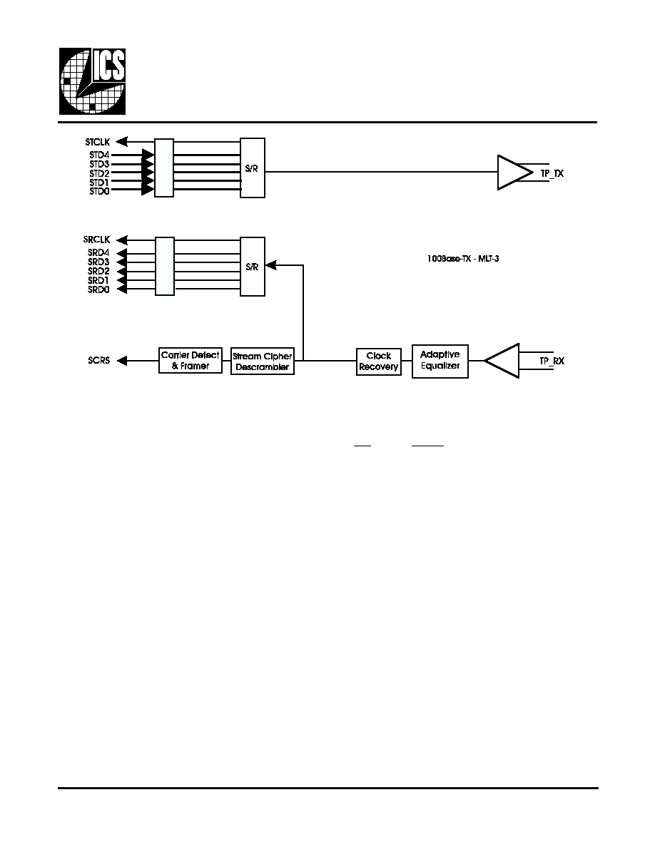
39
ICS1890
100M Stream Interface
100M Stream Interface - Pin Mapping
When the ICS1890 is operating in the stream mode, the MII
Data Interface is remapped to accommodate the 100M Stream
Interface. The following table details the exact pin mapping.
Each individual pin description also contains the new 100M
Stream Interface pseudo pin name followed by the real MII
Data Interface pin name that it is mapped onto.
100M Stream Interface provides a lower latency parallel
interface producing an AMD PDR/PDT and twister type 5 bit
unscrambled interface when the data is scrambled by the
upper layer.
MII
Stream
TXCLK
STCLK
TXEN
(1)
TXER
STD4
TXD3
STD3
TXD2
STD2
TXD1
STD1
TXD0
STD0
RXCLK
SRCLK
RXDV
(2)
RXER
SRD4
RXD3
SRD3
RXD2
SRD2
RXD1
SRD1
RXD0
SRD0
CRS
SCRS
COL
(3)
LSTA
SD

40
ICS1890
(1) 100Base-TX is a continuous transmission system and the
MAC/Repeater is responsible for sourcing IDLE symbols when
it is not transmitting data when using the Stream Interface.
(2) Since data is not framed when this interface is used, RXDV
has no meaning.
(3) Since the MAC/Repeater is responsible for sourcing both
active and idle data, the PHY can not tell when it is transmitting
in the traditional sense so collisions can not be detected.
Other mode configuration pins behave identically regardless
of which data interface is used.
Transmit Clock
STCLK/(TXCLK)
The Transmit Clock (STCLK) is a continuous clock signal
generated by the ICS1890 to synchronize the Transmit Data
lines. In the 100M Stream Interface mode, the ICS1890
clock frequency is 25 MHz.
Transmit Data 4
STD4/(TXER)
Transmit Data 4 (STD4) is the most significant bit and is
sampled continuously by the ICS1890 synchronously with
the Transmit Clock.
Transmit Data 3
STD3/(TXD3)
Transmit Data 3 (STD3) is sampled continuously by the
ICS1890 synchronously with the Transmit Clock.
Transmit Data 2
STD2/(TXD2)
Transmit Data 2 (STD2) is sampled continuously by the
ICS1890 synchronously with the Transmit Data Clock.
Transmit Data 1
STD1/(TXD1)
Transmit Data 1 (STD1) is sampled continuously by the
ICS1890 synchronously with the Transmit Clock.
Transmit Data 0
STD0/(TXD0)
Transmit Data 0 (STD0) (the least significant bit) is sampled
continuously by the ICS1890 synchronously with the Transmit
Clock.
Receive Clock
SRCLK/(RXCLK)
The Receive Clock (SRCLK) is sourced by the ICS1890.
There are two possible sources for the Receive Clock (SRCLK).
When a carrier is present on the receive pair, the source is the
recovered clock from the data stream. When no carrier is
present on the receive pair, the source is the Transmit Clock
(STCLK).
The Receive Clock frequency is 25 MHz in the 100M Stream
Interface mode.
Receive Data 4
SRD4/(RXER)
Receive Error (SRD4) is the most significant bit of the receive
data nibble and is continuously asserted by the ICS1890.
Receive Data 3
SRD3/(RXD3)
Receive Data 3 (SRD3) is continuously asserted by the
ICS1890.
Receive Data 2
SRD2/(RXD2)
Receive Data 2 (SRD2) is continuously asserted by the
ICS1890.
Receive Data 1
SRD1/(RXD1)
Receive Data 1 (SRD1) is continuously asserted by the
ICS1890.
Receive Data 0
SRD0/(RXD0)
Receive Data 0 (SRD0) is the least significant bit of the receive
data nibble.
Carrier Sense
SCRS/(CRS)
Carrier Sense is provided in the 100M Stream Interface mode
as a fast receive carrier look-ahead for optional application
use. Carrier is detected using the same circuitry used in the
MII Data Interface mode that is bypassed in this mode.
The ICS1890 asserts Carrier Sense (SCRS) when it detects
that either the transmit or receive lines are non-idle in half
duplex mode. It is de-asserted when both the transmit and
receive lines are non-idle in half duplex mode. SCRS is not
synchronous to either the transmit or receive clocks.
In full duplex mode and repeater mode, SCRS is asserted only
on receive activity.
Signal Detect
SD/(LSTA)
This signal is asserted when the PLL detects 100Base-T activity
on the receive channel.

41
ICS1890
10M Serial Interface
10M Serial Interface - Pin Mapping
When the ICS1890 is operating in the 10M Serial mode, the
MII Data Interface is remapped to accommodate the 10M
Serial Interface. The following table details the exact pin mapping.
Each individual pin description also contains the new 10M
Serial Interface pseudo pin name followed by the real MII
Data Interface pin name that it is mapped onto.
MII
10M Serial
TXCLK
10TCLK
TXEN
10TXEN
TXER
(1)
TXD3
TXD2
XD1
TXD0
10TD
RXCLK
10RCLK
RXDV
10RXDV
RXER
(1)
RXD3
RXD2
RXD1
RXD0
10RD
CRS
10CRS
COL
10COL
LSTA
LSTA
(1) Error generation and detection is not supported by 10Base-
T. Other mode configuration pins behave identically regardless
of which data interface is used.
Transmit Clock
10TCLK/(TXCLK)
The Transmit Clock (10TCLK) is a continuous clock signal
generated by the ICS1890 to synchronize the Transmit Data
lines. In the 10M Serial Interface mode, the ICS1890 clock
frequency is 10 MHz.
Transmit Enable
10TXEN/(TXEN)
Transmit Enable (10TXEN) indicates to the ICS1890 that the
MAC is sending valid data nibbles for transmission on the
physical media. Synchronous with its assertion, the ICS1890
will begin reading the serial data on the transmit data line. The
ICS1890 terminates transmission of data following the de-
assertion of Transmit Enable.
Transmit Data
10TD/(TXD0)
Transmit Data 0 (10TD) is the serial transmit data bit and is
sampled continuously by the ICS1890 synchronously with
the Transmit Clock.
Receive Clock
10RCLK/(RXCLK)
The Receive Clock (10RCLK) is sourced by the ICS1890 and
is 10 MHz in frequency. There are two possible sources for the
Receive Clock. When a carrier is present on the receive pair,
the source is the recovered clock from the data stream. When
no carrier is present on the receive pair, the source is the
Transmit Clock. In 10Base-T mode, the receive data pair will
be quiescent during periods of inactivity and the Transmit
Clock will be selected.
The ICS1890 will only switch between clock sources when
Receive Data Valid is de-asserted. During the period between
Carrier Sense (CRS) being asserted and Receive Data Valid
being asserted, a clock phase change of up to 360 degrees
may occur. Following the de-assertion of Receive Data valid, a
clock phase of 360 degrees may occur.
Receive Data Valid
10RXDV/(RXDV)
Receive Data Valid (10RXDV) is generated by the ICS1890.
It indicates that the ICS1890 is recovering serial data on the
Receive Data (10RD) line synchronous with the Receive Data
Clock.
The ICS1890 asserts RXDV when it detects and recovers the
preamble or the start of stream delimiter (SSD) and de-asserts
it following the last data nibble or upon detection of a signal
error. RXDV is synchronous with the Receive Data Clock
(10RCLK).
Receive Data
10RD/(RXD0)
Receive Data 0 (10RD) is the received serial data stream.
Carrier Sense
10CRS/(CRS)
The ICS1890 asserts Carrier Sense (CRS) when it detects
that either the transmit or receive lines are non-idle in half
duplex mode. It is de-asserted when both the transmit and
receive lines are idle in half duplex mode. CRS is not synchronous
to either the transmit or receive clocks.
In full duplex mode and repeater mode, CRS is asserted only
on receive activity.

42
ICS1890
Collision Detected
10COL/(COL)
The ICS1890 asserts Collision Detected (COL) when it
detects a receive carrier (non idle condition while transmitting
(TXEN asserted).
In the 10 Mbps mode, the non-idle condition is detected by
monitoring the un-squelched receive signal. COL is not
synchronous to either the transmit or receive clocks.
In full duplex mode, COL is disabled and always remains low.
In the 10 Mbps Node mode, COL will also be asserted as part
of the signal quality error test (SQE). This behavior can be
suppressed with the SQE Test Inhibit bit (18:2).
Link Pulse Interface
Link Pulse Interface - Pin Mapping
When the ICS1890 is operating in the Link Pulse mode, the
MII Data Interface is remapped to accommodate the Link
Pulse Interface. The following table details the exact pin mapping.
Each individual pin description also contains the new Link
Pulse Interface pseudo pin name followed by the real MII
Data Interface pin name that it is mapped onto.
MII
Link Pulse
TXCLK
LTCLK
TXEN
TXER
LPTX
TXD3
TXD2
XD1
TXD0
RXCL
K LRCLK
RXDV
RXER
LPRX
RXD3
RXD2
RXD1
RXD0
CRS
COL
LSTA
SD
Other mode configuration pins behave identically regardless
of which data interface is used.
Transmit Clock
LTCLK/(TXCLK)
The Transmit Clock (10TCLK) is a continuous clock signal
generated by the ICS1890 with a frequency of 25 MHz.
Transmit Link Pulse
LPTX/(TXER)
Data presented on this input will be transmitted as a Link Pulse
of approximately the same duration.
Receive Clock
LRCLK/(RXCLK)
The Receive Clock (LRCLK) is sourced by the ICS1890 and
is 25 MHz in frequency.
Receive Link Pulse
LPRX/(RXER)
Receive activity that is qualified as a Link Pulse will be output
on this pin as a high level of approximately the same duration
as the Link Pulse.
Signal Detect
SD/(LSTA)
This signal is asserted when the PLL detects 100Base-T activity
on the receive channel.

43
ICS1890
MII Management Interface
Management Data Clock
MDC
The Management Data Clock (MDC) is used by the ICS1890
to synchronize the transfer of management information to or
from the ICS1890 using the serial MDIO data line.
Management Data Input/Output
MDIO
The Management Data Input/Output (MDIO) is a tri-statable
line driven by station management to transfer command
information or driven by the ICS1890 to transfer status
information. All transfers and sampling are synchronous with
MDC. If the ICS1890 is to be used in an application which
uses the mechanical MII specification, MDIO must have a
1.5K
±5% pull-up at the ICS1890 end and a 2K
±5% pull-
down at the station management end. This enables station
management to deter-mine if the connection is intact.
Twisted Pair Interface
Transmit Pair
TP_TX+ & TP_TX-
The Transmit pair TP_TX+ and TP_TX- carries the serial bit
stream for transmission over the UTP cable. The current-
driven differential driver is programmed to produce two-level
(10Base-T, Manchester) or three-level (100Base-TX, MLT-3)
signals depending on the mode of operation selected (manually
or by Auto-Negotiation). These output signals interface directly
with an isolation transformer.
Note that these pins may be tristated using the TPTRI control
pin.
Receive Pair
TP_RX+ & TP_RX-
The Receive pair TP_RX+ and TP_RX- carries the serial bit
stream from the mandatory isolation transformer. The serial bit
stream may be two-level (10Base-T, Manchester) or three-
level (100Base-TX, MLT-3) signals depending on the ICS
mode of operation
10M Transmit Current Set Resistor
10TCSR
A resistor is required to be connected between this pin and
the nearest transmit ground to set the value of the transmit
current used in 10M mode.
The value and tolerance of this resistor is specified in the
Electricals section.
100M Transmit Current Set Resistor
100TCSR
A resistor is required to be connected between this pin and
the nearest transmit ground to set the value of the transmit
current used in 100M mode.
The value and tolerance of this resistor is specified in the
Electricals section.
Clock Reference Interface
Frequency Reference
(REF_IN & REF_OUT)
These pins connect to the 25 MHz crystal or the frequency
reference source.
When a frequency reference source like a crystal oscillator
module is used, its output should be connected to REF_IN
and REF_OUT should be left unconnected.
Configuration and Status Interface
Node/Repeater Mode
NOD/REP
When this input is logic zero, the device will default to Node
operation. SQE test will default to on for 10Base-T.
When this input is logic one, the device will default to Repeater
operation. SQE test will default to off and Carrier Sense will be
determined by receive activity only.
This pin setting also affects which clock, TXCLK or REF_IN,
is used to latch the transmit data, TXD. See the description of
the ITCLS pin for the details.
MII Data/Stream Interface Select
MII/SI
This input pin selects the MAC to PHY interface to be used.
When the input is low the MII Data Interface is selected.
When this input is high, the Stream Interface is selected.
The Stream Interface that is used depends on the settings
of the 10/100SEL and 10/LP pins which allow selection of the
100M Stream Interface, 10M/Serial Interface, or Link Pulse
Interface.
10M Serial/Link Pulse Interface Select
10/LP
This input selects between the 10M Serial and Link Pulse
Interfaces when Stream Interface mode is selected with the
MII/SI pin. When this input is low and Stream Interface mode
is selected, the 10M Serial Interface is selected. When this
input is high and Stream Interface mode is selected, the Link
Pulse Interface is selected.

44
ICS1890
When configuration through Auto-Negotiation is selected,
the DPXSEL and 10/100SEL settings control the Auto-
Negotiation register 4 default settings and Auto-Negotiation
is enabled. When configuration without Auto-Negotiation is
selected DPXSEL controls the duplex setting and 10/100SEL
controls the data rate setting.
When this pin is a logic one, software bits have priority over
hardware pin settings. The 10/100SEL pin becomes an output
indicating the link speed when the link is established and
parallels bit (17:15). The DPXSEL pin becomes an output
indicating the link duplex state when the link is established
and parallels bit (17:14). The ANSEL pin becomes an output
indicating whether auto-negotiation is being used and parallels
bit (0:12).
10/100 Select
10/100SEL
This pin is an input or an output depending on the setting of
the HW/SW pin.
In HW mode, it is an input and controls speed selection
directly or through Auto-Negotiation. When the input is low,
10Base-T is selected. When the input is high, 100Base-TX is
selected.
In SW mode, this pin is an output and correctly reflects the
selected speed when the link is established (LSTA is asserted).
The output is low when 10Base-T is selected and high when
100Base-TX is selected which gives the same indication as
register bit (17:15).
Note this pin also affects the MAC - PHY interface that is used
in conjunction with the MII/SI pin.
Duplex Select
DPXSEL
This pin is an input or an output depending on the setting of
the HW/SW pin.
In HW mode, it is an input and controls duplex selection
directly or through Auto-Negotiation. When the input is low,
Half Duplex is selected. When the input is high, Full Duplex is
selected.
In SW mode, this pin is an output and correctly reflects the
selected duplex mode when the link is established (LSTA is
asserted). The output is low when Half Duplex is selected and
high when Full Duplex is selected which gives the same indication
as register bit (17:14).
In Full Duplex mode, CRS is asserted only on receive activity.
In Full Duplex mode, COL is disabled and always remains low.
Auto-Negotiation Select
ANSEL
This pin is an input or output depending on the setting of the
HW/SW pin.
In HW mode, it is an input and controls the enabling of Auto-
Negotiation. When the input is low, Auto-Negotiation is disabled.
When the input is high, Auto-Negotiation is enabled and the
single technology selected by 10/100SEL and DPXSEL is
advertised.
In SW mode, this pin is an output and reflects whether Auto-
Negotiation has been enabled or disabled. The output is low
when Auto-Negotiation is disabled and high when Auto-
Negotiation is enabled which gives the same indication as
register bit (0:12).
Invert Transmit Clock Latching Setting ITCLS~
The ICS1890 allows transmit data to be latched relative to
either TXCLK or REF_IN. Latching the data to TXCLK is the
behavior specified in the 100Base-T MII specification, but in
some applications it is desirable to latch data with the REF_IN
clock. An example of where this might be beneficial is in a
repeater application where all data transmission on multiple
1890s need to be synchronized to a common clock.
To select the proper setting of this pin, first choose the setting
of the NOD/REP pin. Then select the setting of the ITCLS pin
that latches the transmit data with the clock of your choice.
The following table shows the possible combinations. This
pin has an internal pull-up so it may be left not connected for
some applications.
Hardware/Software Priority Select
HW/SW
When this pin is logic zero, hardware pins have priority over
software settings. The 10/100SEL pin becomes an input and
controls speed selection. The DPXSEL pin becomes an input
and controls duplex selection. The ANSEL pin becomes an
input and chooses configuration with or without Auto-Negotiation.
NOD/REP
ITCLS
Latching Clock
NOD
(0)
0
REF_IN
1
TXCLK
REP
(1)
0
TXCLK
1
REF_IN

45
ICS1890
TP_TX Tristate
TPTRI
When this pin is set to a logic zero, the twisted pair transmitter
output pins will be enabled normally to source 100Base-TX or
10Base-T data.
When this pin is set to a logic one, the twisted pair transmitter
output pins will be tristated.
MAC - PHY Receive Interface Tristate
RXTRI
When this input is a logic zero the selected MAC-PHY interface
behaves normally.
When this input is a logic one, the RXCLK, RXD[3:0], RXER,
and RXDV pins are tristated. This allows repeater designs to
bus the shared receive lines without requiring extra tristatable
buffers on each port.
Note that the CRS and COL pins are not tristated. This allows
repeater logic to use these signals to determine which receive
port to enable.
Link Status
LSTA
This output reflects the current Link Status. It is similar to bit
(1:2) but changes dynamically instead of latching on a link
failure. The output is low when the link is invalid and is high
when a valid link has been established.
When this bit is high, the 10/100SEL and DPXSEL bits can be
observed to determine what type of link has been established.
Cipher Locked Status
LOCK
This output reflects the status of the Stream Cipher decoder
block. When the Stream Cipher has not locked onto the incoming
data stream, this output will be a logic zero. When the Stream
Cipher has locked onto the incoming data stream, this output
will be a logic one.
Note that the Stream Cipher will only lock onto 100Base-TX
data (or IDLE symbols) and will not lock when 10Base-T data
is present.
System Reset
RESET~
When grounded, this pin causes the ICS1890 to enter a re-
set/ low power state. On the low to high transition of RESET,
the device will begin to complete its reset cycle. Upon
comple-tion, the ICS1890 will be initialized its default state.
While this pin is held low, the device is kept in its low power
mode. Power savings and timings are shown in the Electricals
section.
LED/PHY Address Usage
The ICS1890 device uses a unique pin sharing scheme that
allows the 5 LED pins to also be used to set the PHY address.
At power-up and reset they define the MII PHY address of the
device. Subsequent to power-up and reset, they become LED
status indicators.
The PHY address can be any number between 0 and 31. When
PHY address 0 is used, the devices MII interface starts out
Isolated and must be enabled through the MII management
port (Reg 0 bit 10), as defined by the IEEE specification. All
other addresses leave the MII interface active.
The actual value used for the individual PHY address bits
depends on the configuration of the LED components. This is
shown in the figure below. When a 1 value is desired the
LED and resistor are connected between the LED pin and Vdd
(LED Pin X). When a 0 value is desired the LED and resistor
are connected between the LED pin and Ground (LED Pin Y).
The special driver will sense the polarity and adjust its drive
logic to appropriately turn the LED light on or off.
Resistor values should be in the range of 510
to 10k
. A
1k
resistor is recommended.
If LEDs are not required for the application, only a resistor is
required to set the PHY address.
If LEDs are not required for the application and the ICS1890
will not be accessed with the serial MII management interface,
then only a single resistor to VDD on any one of the LED pins
is required. This will ensure that the PHY address is not zero,
which would cause the ICS1890 to power up in the isolated
state with no way for management to enable the MII interface.

46
ICS1890
Phy Address 4 - Receive Data LED
P4RD
At power-up and reset, this pin is sampled for a logic high or
zero. If a logic one is detected, a value of 16 is set in the
configuration register.
The ICS1890 sets this bit to the appropriate value to turn on
the LED when receive data is detected. This signal is stretched
ensure that a single packet will be seen. If the packet stream
is continuous, the LED will appear permanently on.
Phy Address 3 - Transmit Data LED
P3TD
At power-up and reset, this pin is sampled for a logic high or
zero. If a logic one is detected, a value of 8 is set in the
configuration register.
The ICS1890 sets this bit to the appropriate value to turn on
the LED when transmit data is detected. This signal is stretched
to ensure that a single packet will be seen. If the packet stream
is continuous, the LED will appear permanently on.
Phy Address 2 - Link Integrity LED
P2LI
At power-up and reset, this pin is sampled for a logic high or
zero. If a logic one is detected, a value of 4 is set in the
configuration register.
The ICS1890 sets this bit to the appropriate value to turn on
the LED when the Link Integrity status is OK.
Phy Address 1 - Collision LED
P1CL
At power-up and reset, this pin is sampled for a logic high or
zero. If a logic one is detected, a value of 2 is set in the
configuration register.
The ICS1890 sets this bit to the appropriate value to turn on
the LED when a collision is detected. This signal is stretched
to ensure that a single collision will be seen. If the collisions
are continuous, the LED will appear permanently on.
Phy Address 0 - Activity LED
P0AC
At power-up and reset, this pin is sampled for a logic high or
zero. If a logic one is detected, a value of 1 is set in the
configuration register.
The ICS1890 sets this bit to the appropriate value to turn on
the LED when either transmit or receive activity is detected.
This signal is stretched to ensure that a single activity event
will be seen. If the activity is continuous, the LED will appear
permanently on.
Power Supply
These 7 VDD and 8 VSS pins supply power to the ICS1890 device.
ICS1890 Power Supply Isolation and Filtering
It is important to properly isolate the ICS1890 10/100Base-
TX Physical Layer Device from noise sources in a system
design. There are two key areas to consider, isolation from
digital noise and noise coupling between the transmitter and
receiver.
Filtering for the ICS1890 is accomplished by separating the
power supply into three domains: digital, transmit, and receive.
All supply pins on the device fall into one of these three
categories as shown in the table below.
In the above table, each supply pin is followed directly by its
ground pin. Each supply pair should be bypassed with a 0.1µF
capacitor located as close to the device as possible.
The PCB board may have separate power and ground planes
for the ICS1890. The power planes could be split into three
domains following the pin isolation. A single, uniform plane
should be used for ground. Power plane placement is illustrated
in the figure below.
Point-to-point trace routing for power connections may be
used instead of actual power planes if required by printed
circuit board constraints.
Both the Receive and Transmit Domains should be connected
to the Digital Domain or main supply through a ferrite bead or
inductor, with a value of .1µH to 1µH. The best filter configuration
is a pi filter composed of a .1µH capacitor, .1µH ferrite bead,
and a .1µH capacitor at the device pin.
Reserved & N/C Pins
Four pins are labeled Reserved or N/C. These pins should
be left unconnected. Connecting these pins to ground or
power may prevent the device from operating properly
Digital Domain
Transmit Domain
Receive Domain
41 VDD 8 VDD
40 VSS 7VSS
16 VDD
18 VDD
17 VSS
54 VDD
51 VSS
56 VDD
55 VSS
25 VDD
29 VSS
57 VDD
63 VSS

47
ICS1890
* Redefined for other MAC-PHY interfaces.
Pin Descriptions
PIN
NUMBER
PIN NAME
I/O
TYPE
Description
1
NOD/REP
I
TTL-compatible
Node/Repeater Mode
2
10/100SEL
I/O
TTL-compatible
10/100 Select
3
10TCSR
I
10M Transmit Current Set Resistor
4
100TCSR
I
100M Transmit Current Set Resistor
5
TP_TX
O
Twisted Pair Transmit Data+
6
TP_TX-
O
Twisted Pair Transmit Data-
7
VSS
8
VDD
Ditigal Domain Power (Transmitter)
9
TPTRI
I
TTL-compatible
Twisted Pair Tristate
10
TP_RX+
I
Twisted Pair Receive Data+
11
TP_RX-
I
Twisted Pair Receive Data-
12
N/C
13
ITCLS~
I
TTL-compatible
Invert Transmit Clock Latching Setting
14
N/C
15
N/C
16
VDD
Receive Domain Power (Receiver)
17
VSS
18
VDD
Receive Domain Power (Receiver)
19
MII/SI
I
TTL-compatible
MII Data/Stream Interface
20
REG
I
TTL-compatible
Ground for high order register access
21
LSTA*
O
TTL-compatible
Link Status
22
RESET~
I
TTL-compatible
System Reset
23
HW/SW
I
TTL-compatible
Hardware/Software Priority
24
DPXSEL
I/O
TTL-compatible
Duplex Select
25
VDD
Receive Domain Power (RPLL)
26
N/C
27
LOCK
O
TTL-compatible
Cipher Lock
28
10/LP
I
TTL-compatible
10M Serial/Link Pulse Interface
29
VSS
30
MDIO
I/O
TTL-compatible
Management Data Input/Output
31
MDC
I
TTL-compatible
Management Data Clock
32
RXD3*
O
TTL-compatible
Receive Data 3

48
ICS1890
Pin Descriptions
* Redefined for other MAC-PHY interfaces.
PIN
NUMBER
PIN NAME
I/O
TYPE
DESCRIPTION
33
RXD2*
O
TTL-compatible
Receive Data 2
34
RXD1*
O
TTL-compatible
Receive Data 1
35
RXD0*
O
TTL-compatible
Receive Data 0
36
RXDV*
O
TTL-compatible
Receive Data Valid
37
RXCLK*
O
TTL-compatible
Receive Clock
38
RXER
O
TTL-compatible
Receive Error
39
RXTRI
I
TTL-compatible
Receive MAC-PHY Interface Tristate
40
VSS
41
VDD
Digital Domain Power
42
TXER*
I
TTL-compatible
Transmit Error
43
TXCLK*
O
TTL-compatible
Transmit Error
44
TXEN*
I
TTL-compatible
Transmit Enable
45
TXD0*
I
TTL-compatible
Transmit Data 0
46
TXD1*
I
TTL-compatible
Transmit Data 1
47
TXD2*
I
TTL-compatible
Transmit Data 2
48
TXD3*
I
TTL-compatible
Transmit Data 3
49
COL*
O
TTL-compatible
Collision Detect
50
CRS*
O
TTL-compatible
Carrier Sense
51
VSS
52
REF_OUT
O
Frequency Reference Output
53
REF_IN
I
CMOS-compatible
Frequency Reference Input
54
VDD
Digital Domain Power
55
VSS
56
VDD
Transmit Domain Power (TPLL)
57
VDD
Digital Domain Power
58
P0AC
I/O
LED
Special PHY ID 0/Activity LED
59
P1CL
I/O
LED
Special PHY ID 1/Collision det LED
60
P2LI
I/O
LED
Special PHY ID 2/Link Integrity LED
61
P3TD
I/O
LED
Special PHY ID 3/Transmit data LED
62
P4RD
I/O
LED
Special PHY ID 4/Receive data LED
63
VSS
64
ANSEL
I/O
TTL-compatible
Auto-Negotiation Select

49
ICS1890
Pin Configuration

50
ICS1890
* CMOS output drive recommended
Recommended Operating Conditions
Recommended Component Values
PARAMETER
SYMBOL
TEST CONDITIONS
MIN
MAX
UNITS
Ambient Operating Temp.
TA
0
+70
∞C
Power Supply
VSS
VDD
0.0
+4.75
0.0
+5.25
V
V
Absolute Maximum Ratings
V
DD
(measured to V
SS
) . . . . . . . . . . . . . . . . . . . . . . . 7.0V
Digital Inputs/Outputs . . . . . . . . . . . . . . . . . . . . . . . . V
SS
-0.5 to V
DD
+0.5V
Storage Temperature. . . . . . . . . . . . . . . . . . . . . . . . . . -65 to 150∞C
Junction Temperature . . . . . . . . . . . . . . . . . . . . . . . . . 175∞C
Soldering Temperature . . . . . . . . . . . . . . . . . . . . . . . . 260∞C
Stresses above those listed under Absolute Maximum Ratings may cause permanent damage to the device. This is a stress rating
only and functional operation of the device at these or any other conditions above those indicated in the operational sections
of the specifications is not implied. Exposure to absolute maximum rating conditions for extended periods may affect product
reliability. Electrical parameters are guaranteed only over the recommended operating temperature range.
Note: This matches the IEEE requirement in the 100Base-X standard definition for the code-bit-timer (24.2.3.4)
which is more stringent than the basic media independent interface (MII) specification for the TX_CLK of
±100ppm (22.2.2.1).
PARAMETER
MIN
TYP
MAX
UNITS
Crystal Oscillator Frequency*
25
MHz
Crystal Oscillator Frequency Tolerance
-50
+50
ppm
10TCSR Resistor Value
1.4
2.0
2.61
K
100TCSR Resistor Value
6.49
6.81
7.50
K
LED Resistor Value
510
1000
10,000

51
ICS1890
DC Characteristics
V
DD
= V
MIN
to V
MAX
, V
SS
= OV, T
A
= T
MIN
to T
MAX
TTL Input/Output
REF_IN Input
Note: REF_IN Input switch point is 50% of VDD.
PARAMETER (condition)
MIN
TYP
MAX
UNITS
MII Input Pin Capacitance
-
8
-
pF
MII Output Pin Capacitance
-
14
-
pF
MII Output Pin Impedance
-
38
-
Ohms
PARAMETER
SYMBOL
CONDITIONS
MIN
MAX
UNITS
IC Supply Current
I
DD
V
DD
=5.25V
-
195
mA
PARAMETER
SYMBOL
CONDITIONS
MIN
MAX
UNITS
TTL Input High Voltage
V
IH
VDD=5V, VSS=0V
2.0
-
V
TTL Input Low Voltage
V
IL
VDD=5V, VSS=0V
-
0.8
V
TTL Output High Voltage
V
OH
VDD=5V, VSS=0V
2.4
-
V
TTL Output Low Voltage
V
OL
VDD=5V, VSS=0V
-
0.4
V
TTL Driving CMOS, Output High Voltage
V
OH
VDD=5V, VSS=0V
3.68
-
V
TTL Driving CMOS, Output Low Voltage
V
OL
VDD=5V, VSS=0V
-
0.4
V
TTL/CMOS Output Sink Current
I
OL
VDD=5V, VSS=0V
8
-
mA
TTL/CMOS Output Source Current
I
OH
VDD=5V, VSS=0V
-
-0.4
mA
PARAMETER
SYMBOL
CONDITIONS
MIN
MAX
UNITS
Input High Voltage
V
IH
VDD=5V, VSS=0V
3.5
-
V
Input Low Voltage
V
IL
VDD=5V, VSS=0V
-
1.5
V
Note: Total system operating current will include load current required by the Tx transformer.

52
ICS1890
Clock - Reference In (REF_IN)
Note: REF_IN switching point is 50% of VDD.
T#
PARAMETER (condition)
MIN
TYP
MAX
UNITS
t1
REF_IN Duty Cycle
45
50
55
%
t2
REF_IN Period
-
40
-
ns

53
ICS1890
MII - Transmit Clock Tolerance
Note: TXCLK Duty Cycle = REF_IN Duty Cycle ±5%.
MII - Receive Clock Behavior
T#
PARAMETER (condition)
MIN
TYP
MAX
UNITS
t1
TXCLK Duty Cycle
35
50
65
%
t2a
TXCLK Period (100Base-T/MII Interface)
-
40
-
ns
t2b
TXCLK Period (10Base-T/MII Interface)
-
400
-
ns
t2c
TXCLK Period (100Base-T/100M Stream Interface)
-
40
-
ns
t2d
TXCLK Period (10Base-T/10M Serial Interface)
-
100
-
ns
T#
PARAMETER (condition)
MIN
TYP
MAX
UNITS
t1
RXCLK Duty Cycle
45
50
55
%
t2a
RXCLK Period (100Base-T/MII Interface)
-
40
-
ns
t2b
RXCLK Period (10Base-T/MII Interface)
-
400
ns
t2c
RXCLK Period (100Base-T/100M Stream Interface)
-
40
ns
t2d
RXCLK Period (10Base-T/10M Serial Interface)
-
100
ns
t4
RXDV Asserted Nominal Clock to Recovered Clock
Cycle Extension
-
-
65
ns

54
ICS1890
MII/100M Stream - Synchronous Transmit Timing
MII/100M Stream - Synchronous Receive Timing
T#
PARAMETER (condition)
MIN
TYP
MAX
UNITS
t1
TXD, TXEN, TXER Setup to TXCLK rise
10
-
-
ns
t2
TXD, TXEN, TXER Hold after TXCLK rise
0
-
-
ns
T#
PARAMETER (condition)
MIN
TYP
MAX
UNITS
t1
RXD, RXDV, RXER Setup to RXCLK rise
10.0
-
-
ns
t2
RXD, RXDV, RXER Hold after RXCLK rise
10.0
-
-
ns
Note: With ITCLS low (or in repeater mode) timing is with respect to REF_IN

55
ICS1890
MII - Management Interface Timing
T#
PARAMETER (condition)
MIN
TYP
MAX
UNITS
t1
MDC Minimum High Time
160
-
-
ns
t2
MDC Minimum Low Time
160
-
-
ns
t3
MDC Period
400
-
-
ns
t4
MDC rise to MDIO valid
0
-
300
ns
t5
MDIO Setup to MDC
10
-
-
ns
t6
MDIO Hold after MDC
10
-
-
ns
t7
Maximum allowable frequency (50pF Loading)
-
-
10
MHz

56
ICS1890
Receive Latency (10M Serial)
T#
PARAMETER (condition)
MIN
TYP
MAX
UNITS
t1
TP_RX input to 10RD delay
(10M Serial Interface)
15
-
16.5
bits
Receive Latency (10M MII)
T#
PARAMETER (condition)
MIN
TYP
MAX
UNITS
t1
1st bit of /5/ on TP_RX to /5/ on RXD
(10M MII)
18
-
19.5
bits

57
ICS1890
Transmit Latency (10M Serial)
T#
PARAMETER (condition)
MIN
TYP
MAX
UNITS
t1
10TD in to TP_TX out delay
(10M Serial Interface)
-
1.5
-
bits
Transmit Latency (10M MII)
T#
PARAMETER (condition)
MIN
TYP
MAX
UNITS
t1
TXD sampled to MDI Output of 1st bit
(10M MII)
-
1.5
-
bits

58
ICS1890
Transmit Latency (MII/100M Stream)
* Note that the IEEE maximum is 18 bits.
T#
PARAMETER (condition)
MIN
TYP
MAX
UNITS
t1
TXEN sampled to MDI Output 1st bit of /J/ (MII IF)*
-
-
4BT
bits
t2
TXD sampled to MDI Output of 1st bit (100M Stream IF)
-
-
5
bits

59
ICS1890
MII - Carrier Assertion/De-assertion on Transmission
MII - Receive Latency (MII/100M Stream)
* Note that the IEEE maximum is 23 bits.
T#
PARAMETER (condition)
MIN
TYP
MAX
UNITS
t1
TXEN sampled to CRS assert
0
-
4
bits
t2
TXD sampled to CRS de-assert
0
-
4
bits
T#
PARAMETER (condition)
MIN
TYP
MAX
UNITS
t1
1st bit of /J/ into TP_RX to /J/ on RXD (100M MII IF)
-
-
19BT
bits
t2
1st bit of /J/ into TP_RX to /J/ on RXD (100M Stream IF)
-
-
12.5
bits

60
ICS1890
MDI Input to Carrier Assertion/De-assertion
* Note that the IEEE maximum is 20 bit times.
** Note that the IEEE minimum is 13 bit times and the maximum is 24 bit times.
T#
PARAMETER (condition)
MIN
TYP
MAX
UNITS
t1
1st bit of /J/ into TP_RX to CRS assert*
-
-
124ns/13BT
bits
t2
1st bit of /J/ into TP_RX while transmitting data to
COL assert (Half Duplex Mode)*
-
-
13
bits
t3
First bit of /T/ into TP_RX to CRS de-assert**
-
-
130ns/13BT
bits
t4
First bit of /T/ received into TP_RX to COL de-
assert (Half Duplex Mode)**
-
-
14
bits

61
ICS1890
Reset - Power on Reset
Reset - Hardware Reset & Power-down
T#
PARAMETER (condition)
MIN
TYP
MAX
UNITS
t1
VDD to 4.5V to Reset Complete
-
-
20
µs
T#
PARAMETER (condition)
MIN
TYP
MAX
UNITS
t1
RESET active to device isolation and initialization
-
-
200
ns
t2
Minimum RESET pulse width
80
-
-
ns
t3
RESET released to device ready
-
-
640
ns

62
ICS1890
10Base-T Heartbeat Timing
10Base-T Jabber Timing
T#
PARAMETER (condition)
MIN
TYP
MAX
UNITS
t1
COL Heartbeat assertion delay from TXEN de-assertion
(10Base-T Half Duplex)
-
-
1210
ns
t2
COL Heartbeat assertion duration (10Base-T Half Duplex)
-
-
1170
ns
T#
PARAMETER (condition)
MIN
TYP
MAX
UNITS
t1
Jabber activation time (10Base-T Half Duplex)
-
26
-
ms
t2
Jabber deactivation time (10Base-T Half Duplex)
-
410
-
ms

63
ICS1890
10Base-T Normal Link Pulse Timing
Auto-Negotiation Fast Link Pulse Timing
T#
PARAMETER (condition)
MIN
TYP
MAX
UNITS
t1
Normal Link Pulse Width (10Base-T)
-
100
-
ns
t2
COL Heartbeat assertion duration (10Base-T Half Duplex)
8
-
24
ms
T#
PARAMETER (condition)
MIN
TYP
MAX
UNITS
t1
Clock/Data pulse width
-
100
-
ns
t2
Clock pulse to Data pulse timing
55.5
62.5
69.5
µs
t3
Clock pulse to Clock pulse
111
125
139
µs
t4
FLP Burst width
-
2
-
ms
t5
FLP burst to FLP burst timing
8
16
24
ms
t6
Number of Clock/Data pulses in a burst
17
-
33
pulses

64
ICS1890
T#
PARAMETER (condition)
MIN
TYP
MAX
UNITS
t1
Ideal data recovery window
-
-
8
ns
t2
Actual data recovery window
6
-
8
ns
t3
Data recovery window truncation
0
-
1
ns
t4
SD assert to data acquired
-
-
100
ns
Clock Recovery

65
ICS1890
* Repeaters and Hubs are generally responsible for including a cable crossover. One way of doing this is to exchange
transmit (1 & 2) and receive (3 & 6) connections to the RJ-45.
** A minimum of 2KV capacitor should be used to make the connection to the chasis ground.
*** These are close starting values. These resistors need to be tailored to individual system insertion losses, these values
can go as low as 1K
. Average 10TCSR value (pin 3) is 1.91K
.
The following magnetics modules have been tested with the ICS1890
PHYceiver and have been found to perform acceptably.
Nano Pulse (NPI)
Pulse
Valor
Bell Fuse
Halo
Innet
Unicom
NP16120-30
PE-68517
ST6114
S558-5999-01
TG22-SO10ND
T0027S
2HT16-27
Manufacture
Extra Choke Type
NP16170-30
PE-68515
STG118
S558-5999-00
TG22-SO20ND
T0019S
Without Extra Choke Type

66
ICS1890
TQFP/MQFP Package
Dimensions in millimeters.
DIMENSION NAME
LEAD COUNT (N) 64L
TQFP
MQFP
BODY THICKNESS
1.4
2.7
FOOTPRINT (BODY+) Nominal
2.0
3.20
DIMENSIONS
TOLERANCE
TQFP
TOLERANCE
MQFP
Full Package Height
A
MAX.
MAX.
1.60
3.00
Package Standoff
A
1
MAX.
MAX.
0.15
0.25
Package Thickness
A
2
±0.05
+0.10/-0.05
1.4
2.7
Tip-to-Tip Width
D
BASIC
±0.25
16.0
17.20
Body Width
D
1
BASIC
±0.10
14.0
14.00
Tip-to-Tip Width
E
BASIC
±0.25
16.0
17.20
Body Width
E1
BASIC
±0.10
14.0
14.00
Footlength
L
±0.15
+0.10/-0.10
0.60
0.88
Lead Pitch
e
BASIC
BASIC
0.80
0. 80
Lead Width w/Plate
B
+0.08/-0.05
+0.10/-0.05
0.37
0.35
Lead Height w/Plate
*
+0.04/-0.07
MAX.
0.16
0.23
ICS reserves the right to make changes in the device data identified in this publication
without further notice. ICS advises its customers to obtain the latest version of all
device data to verify that any information being relied upon by the customer is current
and accurate.
Ordering Information
ICS1890Y
ICS1890Y-14
ICS XXXX Y
Example:
Package Type
Y=MQFP Y-14=TQFP
Device Type (consists of 3 or 4 digit numbers)
ICS, AV=Standard Device
Prefix