 | –≠–ª–µ–∫—Ç—Ä–æ–Ω–Ω—ã–π –∫–æ–º–ø–æ–Ω–µ–Ω—Ç: ICS2008BY | –°–∫–∞—á–∞—Ç—å:  PDF PDF  ZIP ZIP |

Integrated
Circuit
Systems, Inc.
General Description
Features
ICS2008B
ICS2008B Rev B 6/6/01
Block Diagram
SMPTE Time Code Receiver/ Generator
∑
Internal and external sync sources
≠ Genlock to video or house sync inputs
≠ Internally generated timing from oscillator input
≠ External click input
∑
LTC and VITC Generators
≠ Real Time SMPTE Rates: 30 Hz, 29.97 Hz,
25 Hz, 24 Hz
≠ Time Code Modes: Drop Frame and Color Frame
≠ VITC can be inserted on two lines from 10-40
(SMPTE specifies lines 10-20)
≠ Jam Sync, freewheeling, error bypass/correction,
and plus-one-frame capability
∑
LTC Receiver
≠ Meets SMPTE and EBU LTC specifications
≠ Synchronize bit rates from 1/30
th
nominal to 80X
nominal playback speed.
∑
VITC Receiver
≠ Reads code from any or all selected scan lines.
≠ Meets SMPTE VITC specifications
New, Improved Features
∑
Time Code Burn-in Window with programmable
position, size and character attributes
∑
Internal Timer, allows 1/4 Frame MIDI Time Code
Messages
∑
LTC edge rate control, conforms to EBU Tr and Tf
specification
∑
Improved video timing lock during VCR pause and
shuttle modes
∑
VITC search mode, will search through VBI lines until
VITC is found
∑
New UART frequency of 38.4 K baud for tape transport
control
∑
Improved video output performance
The ICS2008B, SMPTE Time Code Receiver / Generator
chip, is a VLSI device designed in a low power CMOS
process. This device provides the timing coordination for
Multimedia sight and sound events. Although it is aimed at
a PC Multimedia environment, the ICS2008B is easily
integrated into products requiring SMPTE time code
generation and/or reception in LTC (Longitudinal Time
Code) and/or VITC (Vertical Interval Time Code) formats
and MTC (MIDI Time Code) translation.
Taking its input from composite video, S-Video, or an
audio track, the ICS2008B can read SMPTE time code in
VITC and LTC formats. Time code output formats are LTC
and VITC. All are available simultaneously. A UART is
provided for the user to support MTC or tape transport
control.
The processor interface is compatible with the IBM PC and
ISA bus compatible computers and is easily interfaced to
other processors.
The ICS2008B is an improved version of the ICS2008,
with additional features and capabilities.
ICS2008 ICS2008B 2008 2008B
ICS reserves the right to make changes in the device data identified in
this publication without further notice. ICS advises its customers to
obtain the latest version of all device data to verify that any
information being relied upon by the customer is current and accurate.
ICS2008B
2
ICS2008B Rev B 6/6/01
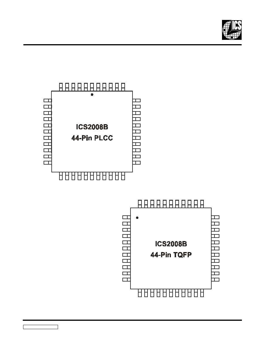
Package Pinouts
18 19 20 21 22 23 24 25 26 27 28
29
30
31
32
33
34
36
38
35
37
39
6
5
4
3
2
1
40
41
42
43
44
D2
D1
D0
IOW *
VDD
VSS
IOR*
UARTCS*
SM PTECS*
A1
A0
Y
1
S
T
H
R
E
S
H
C
T
H
R
E
S
H
D
T
H
R
E
S
H
R
X
D
C
T
S
*
T
X
D
R
T
S
*
L
R
C
L
K
V
I
T
C
G
A
T
E
V
I
T
C
O
U
T
LTCOUT
LFC
XTAL2
XTAL1
AVDD
AVSS
COUT
YOUT
C2
Y2
C1
D
4
L
T
C
I
N
+
D
3
L
T
C
I
N
-
C
L
I
C
K
F
R
A
M
E
R
E
S
E
T
I
N
T
R
D
7
D
6
D
5
7
8
9
10
11
12
13
14
15
16
17
12 13 14 15 16 17 18 19 20 21 22
23
24
25
26
27
28
30
32
29
31
33
44 43 42 41 40 39
34
35
36
37
38
D2
D1
D0
IOW *
VDD
VSS
IOR*
UARTCS*
SM PTECS*
A1
A0
Y
1
S
T
H
R
E
S
H
C
T
H
R
E
S
H
D
T
H
R
E
S
H
R
X
D
C
T
S
*
T
X
D
R
T
S
*
L
R
C
L
K
V
I
T
C
G
A
T
E
V
I
T
C
O
U
T
LTCOUT
LFC
XTAL2
XTAL1
AVDD
AVSS
COUT
YOUT
C2
Y2
C1
D
4
L
T
C
I
N
+
D
3
L
T
C
I
N
-
C
L
I
C
K
F
R
A
M
E
R
E
S
E
T
I
N
T
R
D
7
D
6
D
5
1
2
3
4
5
6
7
8
9
10
11
3
ICS2008B
ICS2008B Rev B 6/6/01
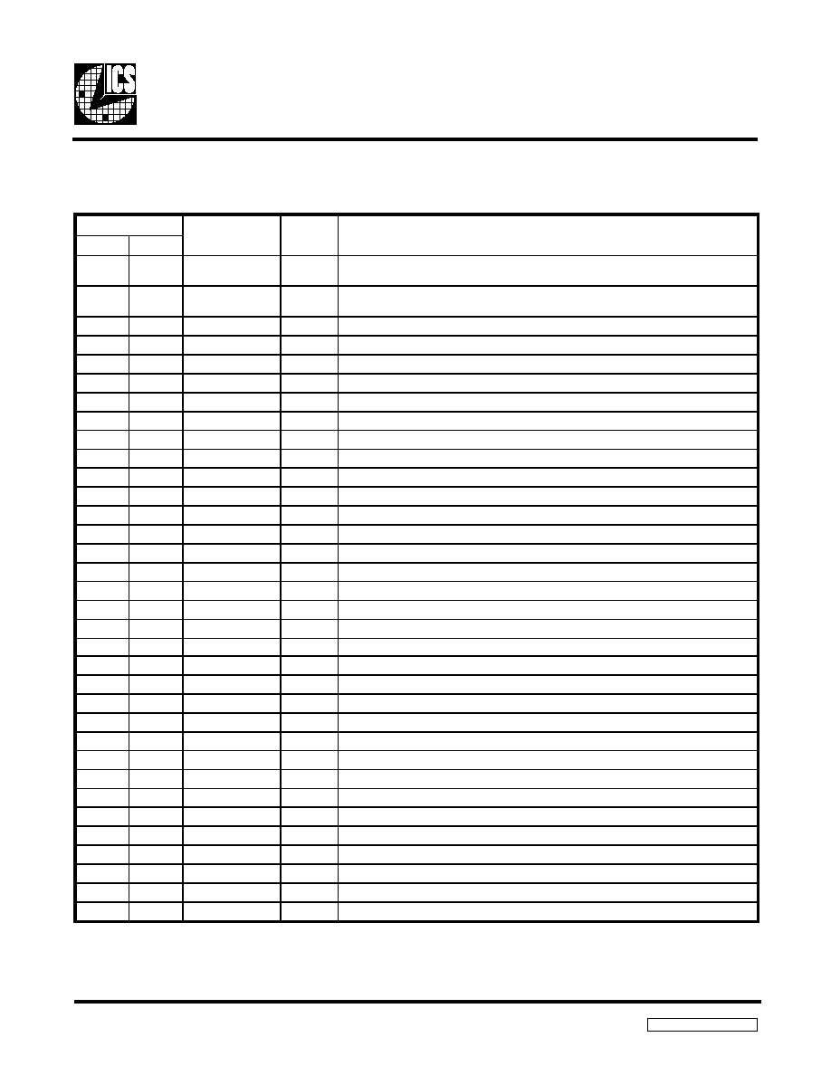
Pin Descriptions
TYPE:
A ≠ Analog ∑ P ≠ Power ∑ I ≠ Input ∑ O ≠ Output
2008 2008B ICS2008
PIN NUMBER
PIN
NAME
TYPE
DES CRI PTI ON
TQFP
PLCC
12, 10
18, 16
Y1, Y2
AI
Video inputs from camera or other source. NOTE: This is also the Y
(Luma) input for S-VHS and HI-8 systems.
11, 9
17, 15
C1, C2
AI
C (Chroma) inputs for S-VHS and HI-8 systems. In NTSC systems, this
pin should be tied to its respective Y input.
15
21
DTHRESH
AI
Data Threshold bypass input.
13
19
STHRESH
AI
SYNC Threshold bypass input.
14
20
CTHRESH
AI
Clamp Threshold bypass input.
8
14
Y OUT
AO
Video output. This is also the Y (Luma) output in S-Video mode.
7
13
C OUT
AO
C (Chroma) output for S-VHS and HI-8 systems.
41
3
FRAME
AI
Color Frame A/B input. This input is self biased (See Applications).
42
4
CLICK
AI
LTC SYNC input. This input is self biased (See Applications).
44
6
LTCIN+
AI
SMPTE LTC input+. This input is self biased (See Applications).
43
5
LTCIN
AI
SMPTE LTC input . This input is self biased (See Applications).
1
7
LTCOUT
AO
SMPTE LTC output
20
26
LRCLK
O
SMPTE LTC receive clock output.
22
28
VITCOUT
O
SMPTE VITC output to video mixer circuit.
21
27
VITCGATE
O
VITC gate indicates VITC code is being output for video overlay.
18
24
TxD
O
UART Transmit data
16
22
RxD
I
UART Receive data
17
23
CTS*
I
Clear to Send
19
25
RTS*
O
Ready to Send
4
10
XTAL1
I
14.318 MHz crystal input.
3
9
XTAL2
O
14.318 MHz crystal oscillator output.
2
8
LFC
AI
Tie to +5 VDC
24, 23
30, 29
A1-A0
I
Address bus
27
33
IOR*
I
Read Enable (active low)
30
36
IOW*
I
Write Enable (active low)
25
31
SMPTECS*
I
SMPTE port chip select (active low)
26
32
UARTCS*
I
UART chip select (active low)
40
2
RESET
I
Master reset (active high)
38 31
44 37
D7-D0
I/O
Bi-directional data bus
39
1
INTR
O
Interrupt Request (active high)
5
11
AVDD
P
Analog V
DD
6
12
AVSS
P
Analog Ground
29
35
VDD
P
Digital V
DD
28
34
VSS
P
Digital

ICS2008B
4
ICS2008B Rev B 6/6/01
Functional Description
The following is a functional description of the hardware regis-
ters in the ICS2008B chip. It also describes how those
registers can be utilized by the software to facilitate specific
application services.
Hardware Environments
The ICS2008B operates as a peripheral to a processor such as
a PC or a single chip microprocessor. Many of the real time
requirements are satisfied by double buffering both incoming
and outgoing time codes.
LTC Input
LTCIN is a differential analog input feeding a comparator
with hysteresis. It requires capacitive coupling to the LTC
source. The output of the comparator goes to the LTC re-
ceiver, which is capable of receiving LTC in a forward or
backward direction at a rate from 1/30
th
to 80X nominal
frame rates. The incoming LTC data is sampled with a phase-
locked clock and loaded into the receive buffer following the
receipt of a valid LTC SYNC pattern. When a complete frame
has been received, an interrupt is generated.
LTC Output
The LTC output can be analog or digital. When set up as an
analog output, it can drive a high impedance load.
The LTC generator outputs a LTC frame at the selected frame
rate, such as 24 Hz, 25 Hz, 29.97 Hz or 30 Hz, and starts the
frame based on a start time generated by the selected LTC
SYNC source.
The output edge rate is programmable for SMPTE code
(25
µ
sec) and EBU code (50
µ
sec) rise and fall times.
Video Inputs
There are two sets of video inputs. In a composite NTSC or
PAL system, the Y input is the only one used. It is capacitively
coupled to the source. In S-Video systems, capacitively couple
Y and C to their respective sources. Proper termination of the
source should be observed. One of the two video sources is
selected by the VIDSEL bit in the SMPTE control registers as
the video SYNC source. Internal timers are synchronized with
the incoming video to extract timing information used to re-
ceive and generate VITC.
The VITC receiver samples the incoming video looking for a
valid VITC code on selected scan lines. When a valid code is
received it is written to a VITC receive buffer. More than one
line can contain VITC code, and the codes can be different. For
this reason, VITC codes from selected lines of a frame are writ-
ten to separate VITC buffers.
Video Output
The video output combines the selected video input with the
outputs from the VITC generator and the character generator.
It can be a composite or an S-Video output as selected by the
SVID bit in the SMPTE control registers.
VITC code is generated from data in the VITC generator
buffer and output during the selected line time(s). The CRC
and synchronizing bits are automatically generated by the
VITC generator, but all of the data fields are sent directly from
the buffer with no modification.
A character generator is provided to insert the time code in a
burn-in window which overlays the incoming video. The ver-
tical and horizontal position of the burn-in window is
programmable.
SMPTE SYNC Sources
A time code generator must have a SYNC input from a stable
source in order to position the LTC code properly on a audio
track of video tape or film. Three SYNC sources, video, click
input, and free running, are available. In the case of a video
tape, LTC code must start within plus or minus one line of the
beginning of line 5. This requires "Genlocking" to the incom-
ing video. The video timing section locks to the video's
horizontal and vertical SYNC signal and generates a SMPTE
SYNC. If some external SYNC source is available it can be
input on the CLICK input. Otherwise, a free running SMPTE
SYNC is generated from the oscillator at the selected frame
rate.
Video Timing Generator
The video timing generator is "Genlocked" to the video
input's SYNC separator. It extracts NTSC or PAL timing in-
formation from the video input and generates line and pixel
rate timing for the VITC receiver, VITC generator, LTC gen-
erator and character generator. If no video input is present, it
generates free running timing.
Overlay Character Generator
It is sometimes desirable to display the time code on a video
display along with the picture. A character generator is pro-
vided for that purpose. The time code display, or burn-in
window, can be positioned anywhere on the screen. It can be
displayed in two sizes with white or black characters on a
black, white or live video background.

5
ICS2008B
ICS2008B Rev B 6/6/01
UART
A general purpose UART is provided for MIDI, video trans-
port control, etc. Most serial interface transport controls use
9600 and 38.4K BAUD. The CTS and RTS modem controls are
needed in these applications. MIDI ports use 31.25K BAUD,
but they do not require modem controls. The receiver includes
a four byte FIFO to reduce the real time interrupt servicing re-
quirements. This is particularly important in MIDI applications
because of the high data rate and the fact that many MIDI mes-
sages are three bytes long. The transmitter is doubled
buffered. Interrupts can be generated on both
receiver data available and/or transmit buffer empty.
Interrupt Timer
The interrupt timer is a general purpose 10 bit timer with three
clock sources (100 kHz, the LTC receive clock and the LTC
transmit clock). Although the timer is general purpose in
nature, its main purpose is to facilitate the timed generation of
MIDI time code messages.
Processor Interface
The ICS2008B supports standard microprocessor interfaces
and busses, such as the PC bus, to allow access to six control/
status and data registers. These six registers are organized into
two groups, one set of four for SMPTE control and the other
set of two for direct UART port control. Each set of registers is
selected with its own chip select, SMPTECS* and UARTCS.*
SMPTE Registers
The SMPTE register set allows access to four direct and
64 indirect registers. The first two direct access registers
addressed at locations 0 and 1 are for status and interrupt con-
trol. The 64 indirect registers are accessed by writing an
indirect address into SMPTE2 and reading from or writing to
SMPTE3. If the AUTOINC bit in SMPTE2 is set to 1, the
indirect register address is automatically incremented after an
access to SMPTE3. This eases the task of reading or writing
sequential indirect locations.
The SMPTE0 Register contains the SMPTE interrupt controls
and status and the VITC read status. The four interrupt bits,
LRI, LXI, VLI and TMI reflect the status of the potential
interrupt sources to the processor. When a bit is set to one and
the corresponding enable bit, LRIEN, LXIEN or VLIEN, is also
set, the INTR output will be activated. Interrupts are cleared by
reading SMPTE0.
LRI -- This bit indicates that a LTC receive interrupt has
occurred. In order for an actual processor interrupt to occur,
the LRIEN bit must also be set. An LRI interrupt occurs upon
reception of the last byte of LTC receive data which was pre-
ceded by a valid LTC SYNC pattern. That is after the 64
th
LTC receive bit time in the forward direction. At normal
frame rates, if the LTC transmitter is synchronized with the
LTC receiver, there is about 3 milliseconds after this interrupt
before the LTC transmit data for the next output frame is
transferred to the output buffer.
LXI -- This bit indicates that a LTC transmit interrupt has
occurred. When this bit is set, and the corresponding LXIEN
bit has been set, the INTR output will be activated. The LTC
transmit interrupt is activated after the transfer of LTC trans-
mit data to the output buffer. This occurs after LTXEN is set to
one and after the 72
nd
LTC transmits bit time of the current
frame, "N." Data loaded after this interrupt will appear in out-
put frame "N+2" since the transmitter is double buffered.
VLI -- This is a status bit that indicates that the video line
selected via the Video Interrupt Line Register, VR9, has
passed. When the VLIEN bit is also set, the processor will be
interrupted. This interrupt can be used by the processor to
determine when to sample the VITC time code when time
locked to a video source. It will also be used to facilitate
detection of LTC time code dropout and off speed LTC code,
e.g. shuttling operations.
TMI -- This bit indicates that a timer interrupt has occurred.
When the TMIEN bit is also set to a one, the INTR output will
be activated. This interrupt is intended to facilitate timing
MIDI clocks and MIDI Quarter Frame messages.
Interrupt Control/Status
LRI (LTC RCV Interrupt)
LXI (LTC XMT Interrupt)
VLI (Video Line Interrupt)
LRIEN (1-enable, 0-disable)
LXIEN (1-enable, 0-disable)
VLIEN (1-enable, 0-disable)
TMI (Timer Interrupt)
TMIEN (1-enable, 0-disable)
7 6 5 4 3 2 1 0
SMPTE0
*
S
C
E
T
P
M
S
1
A
0
A
R
E
T
S
I
G
E
R
0
0
0
s
u
t
a
t
S
/
l
o
r
t
n
o
C
t
p
u
r
r
e
t
n
I
0
E
T
P
M
S
0
0
1
s
u
t
a
t
S
E
T
P
M
S
1
E
T
P
M
S
0
1
0
s
s
e
r
d
d
A
r
e
t
s
i
g
e
R
t
c
e
r
i
d
n
I
2
E
T
P
M
S
0
1
1
a
t
a
D
r
e
t
s
i
g
e
R
t
c
e
r
i
d
n
I
3
E
T
P
M
S

ICS2008B
6
ICS2008B Rev B 6/6/01
The SMPTE Status Register is a read only register which
contains video and LTC status.
FRAMEIN -- This bit indicates the state of the FRAME
input pin. It is used as an alternate source for B/A frame
status. This is useful when the quality of the video signal is
not good enough to extract the B/A frame status.
CLICK -- This bit indicates the state of the CLICK input
pin. It can be used as a synchronization source for the LTC
transmitter.
LTCLOCK -- When a valid forward or backward LTC sync
pattern is detected, this bit is set to one. It is reset to zero when
an expected LTC sync pattern is missed or an invalid LTC bit
is detected.
CODEDIR -- The code direction bit works in conjunction
with the LTCLOCK bit. When the LTCLOCK bit is set to one,
the CODEDIR bit is valid. Otherwise, it is not. See the table
below.
VLOCK -- This is a hardware driven bit which indicates that
genlock has been achieved with the selected video SYNC
source.
FRAME & FIELD -- The hardware SYNC separator detects
the field and frame from the selected video input. The even/
odd fields are identified by a 1/0 in bit 6. Bit 7, FRAME, is
valid for PAL video after line 6. Bit 6, FIELD, is valid after
line 5 in NTSC mode or line 2 in PAL mode.
The SMPTE2 register is the register which points to the 57
indirect registers. When reading or writing an indirect
register, the value in the ADDRESS pointer, SMPTE2 bits 5
to 0, is the address of the register accessed through SMPTE3.
If the AUTOINC bit is set to one, at the end of an access cycle
to SMPTE3, ADDRESS will automatically increment.
Otherwise, ADDRESS holds its value.
SMPTE3 is the data register through which all of the indirect
registers are accessed. The address for a given register must
first be set in SMPTE2 before accessing that register.
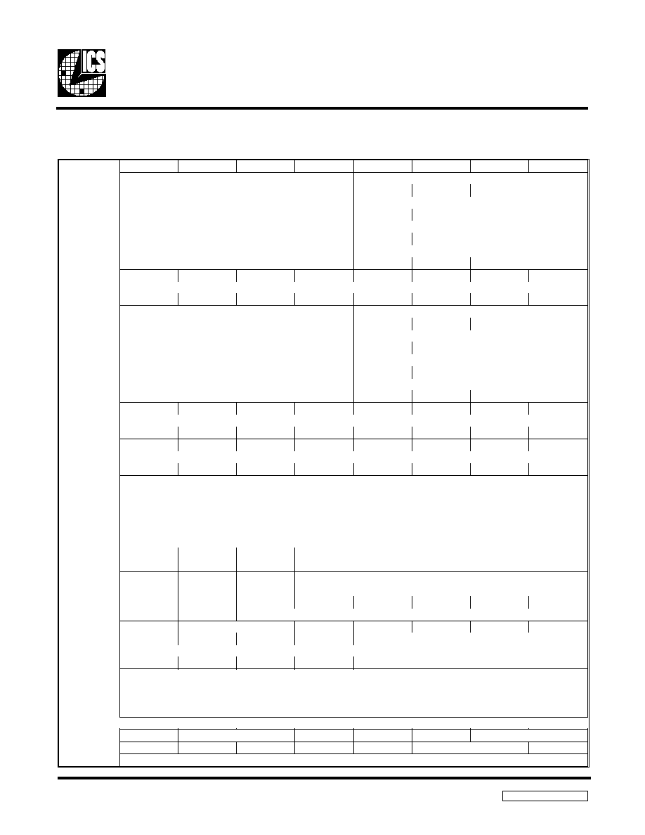
Indirect Registers
The following describes the functions controlled by the
indirect registers. A map of the indirect registers follows this
section, on page 11.
LTC Read Registers IR0-IR7 (read-only)
These read only registers contain the LTC data as received.
Both forward and backward frames are stored with LTC bit 0
in the LSB of IR0 and LTC bit 63 in the MSB of IR7.
LTC Write Registers IR8-IRF
These registers contain the data to be sent by the LTC trans-
mitter. The LSB of IR8 is sent as LTC bit 0, and the MSB of
IRF is sent as LTC bit 63. The data is transmitted as it is stored
in IR8-IRF.
LTCLOCK CODEDIR
LTC RECEIVER STATUS
0
X
Looking for SYNC pattern
1
0
Receiving LTC (FORWARD)
1
1
Receiving LTC (BACKWARD)
SMPTE Status Register
FRAMEIN (input = 1-high, 0-low)
CLICK (input = 1-high, 0-low)
LTCLOCK (1-locked, 0-not locked)
CODEDIR (1-bkwd, 0-fwd)
Reserved
VLOCK (1-locked, 0-not locked)
FIELD
FRAME (PAL only)
7 6 5 4 3 2 1 0
SMPTE1
Indirect Address Register
ADDRESS
Reserved
AUTOINC (1-increment, 0-hold)
SMPTE2
7 6 5 4 3 2 1 0
Indirect Address Register
SMPTE3
7 6 5 4 3 2 1 0

7
ICS2008B
ICS2008B Rev B 6/6/01
VITC Read 1 Registers IR10-IR17 (read-only)
These read only registers contain the VITC data as received
from the video line selected in IR30. The frame is stored with
VITC bit 2 in the LSB of IR10 and VITC bit 80 in the MSB of
IR17. Note that a binary 10 sync pattern precedes every eight
data bits of the VITC frame. The 10 sync pattern is not stored.
The CRC is checked by the VITC receiver, and the result is
reported in IR30.
VITC Read 2 Registers IR18-IR1F (read-only)
As with the VITC Read 1 registers, these read only registers
contain the VITC data as received from the video line selected
in IR31. The frame is stored with VITC bit 2 in the LSB of
IR18 and VITC bit 80 in the MSB of IR1F. The result of the
CRC check is reported in IR31.
VITC Write Registers IR20-IR27
These registers contain the data to be output by the VITC
generator. The VITC frame is output with the LSB of IR20 in
VITC bit 2 and the MSB of IR27 in VITC bit 80. Note that the
binary 10 sync pattern which precedes every eight data bits of
the VITC frame is automatically generated by the VITC
generator. The CRC is also automatically generated by the
VITC generator.
BI Window Registers IR28 & 29
The next two registers control the position of the SMPTE
video display, burn-in, window within the video raster. IR28
selects the video column (horizontal position) in which the
burn-in window starts.
IR29 selects the video line which starts the SMPTE video
display window in the video output. When this register is set
to zero, there will be no Burn-In Window displayed in the
video output.
BI Character Registers IR2A-IR2D
These registers contain the character codes used for the
SMPTE time code in the burn-in window which overlays the
source in the video output. An internal character generator
converts the BCD nibbles to display characters.
ITC Write Line Select Registers IR2E & IR2F
VITC code is normally output on two separate video lines in
each field for redundancy. These two registers allow the indi-
vidual line selection & output enables for the two VITC lines.
Write Line ≠ Selects the video line on which the VITC code
will be output. The video line on which the code is output will
be the number in this register plus 10; e.g. writing a one to this
register will cause the code to be output on line 11.
VITC Write Enable ≠ Enables the output of VITC code on the
specified line.
Burn-in Window Column
Column
IR28
Burn-in Window Line
Line (00 - disable)
IR29
7 6 5 4 3 2 1 0
7 6 5 4 3 2 1 0
7 6 5 4 3 2 1 0
VITC Write Line 1
Write Line #10-40 (N+10)
Reserved
VITC Write Enable (1-enable)
IR2E
7 6 5 4 3 2 1 0
VITC Write Line 2
Write Line #10-40 (N+10)
Reserved
VITC Write Enable (1-enable)
IR2F
Burn-in Window Registers
IR2A
≠ (Frame)
IR2B
≠ (Seconds)
IR2C
≠ (Minutes)
IR2D
≠ (Hours)
7 6 5 4 3 2 1 0
Tens
Ones
E
D
O
C
R
E
T
C
A
R
A
H
C
E
D
O
C
R
E
T
C
A
R
A
H
C
0
0
8
8
1
1
9
9
2
2
A
e
s
U
t
o
N
o
D
3
3
B
?
4
4
C
_
5
5
D
!
6
6
E
"
7
7
F
k
n
a
l
B

ICS2008B
8
ICS2008B Rev B 6/6/01
Video Control Register IR32
GENLOCK ENABLE -- When set to one, this bit enables
the genlock circuits to sync to the selected video input signal.
When reset to 0, the video sync will "freewheel," generating
video timing from the internal oscillator. The freewheel mode
would be selected when striping LTC to allow synchroni-
zation with a MIDI sequencer or other strictly timed audio
source.
VTRES -- When set to one, this bit clears the video timing
counters to dot zero of line 1 of field 1. This is useful when the
video is free running, not genlocked and LTC sync needs to be
synchronized to an event such as the CLICK input.
VSYNCSEL -- When set to one, this bit selects the video
input source from Video2 (Y2) to be the SYNC source for the
internal video timing. Otherwise, when reset to zero, Video1
(Y1) is selected.
VITCSEL -- When set to one, this bit selects the video input
source from Video2 (Y2) to be the VITC time code source for
the VITC receiver. Otherwise, when reset to zero, Video1
(Y1) is selected.
VOUTSEL -- When set to one, this bit selects the video
input source from Video2 (Y2, C2) to be output on the video
outputs (YOUT, COUT). When reset to zero, Video1 (Y1,
C1) are selected.
VID1_S -- When set to one, this bit causes the Video1 source
to be treated as S-Video. Otherwise, when cleared to zero, the
Video1 source is treated as composite video.
VID2_S -- When set to one, this bit causes the Video2 source
to be treated as S-Video. Otherwise, when cleared to zero, the
Video2 source is treated as composite video.
VITC Read Line Select Registers IR30-IR31
As with the VITC Write Line Register, these registers allow
control of the individual redundant VITC read lines. The
processor can also reprogram these dynamically to allow for
scanning of VITC code when the source lines are unknown.
Read Line ≠ Selects the line from which VITC code is to be
read within each field. It works identically to the Write Line
in that the video line selected is the number in this register
plus 10.
Auto line scanning is enabled by writing a 1Fh to the Read
Line field. This causes the VITC reader to search for time
code. If VITC Read Line 1 is set to search, it starts with line
10 and quits when it finds a valid time code or when it reaches
line 41. Searching with VITC Read Line 2 starts after VITC
Read Line 1. In the case of searching for both VITC Read
Lines 1 and 2, VITC Read Line 2 starts searching after the
first valid time code has been found. However, if VITC Read
Line 1 is set to a specific line, VITC Read Line 2 starts after
that specified line regardless of whether valid time code was
received. In any case, the search terminates after line 41.
CRCERR -- This bit is reset to zero when a valid VITC code
has been received. It is valid from the end of the selected
video line until the end of the selected line in the next field.
NOCODE -- This bit is set when a framing error occurs in
the VITC code, i.e. not all the bits of the code were received
by the time the end of the video line occurred. Both CRCERR
and NOCODE must be zero to qualify a VITC code.
Video Control Register
GENLOCK ENABLE (1-lock, 0-freewheel)
VTRES - Video Timing Reset (1-reset)
VSYNCEL - Video SYNC Source Select
VITCSEL - VITC Source Select
VOUTSEL - Video Output Select
VID1_S - Video1 S-Video Select
VID2_S - Video2 S-Video Select
PAL/NTSC (1-PAL, 0-NTSC)
7 6 5 4 3 2 1 0
IR32
VITC Read Line 1
Read Line 10-40 (N+10)
CRCERR (1-error, 0-OK) (r/o)
NOCODE (1-no code, 0-code) (r/o)
VITC Read Enable (1-enable)
IR30
7 6 5 4 3 2 1 0
VITC Read Line 2
Read Line 10-40 (N+10)
CRCERR (1-error, 0-OK) (r/o)
NOCODE (1-no code, 0-code) (r/o)
VITC Read Enable (1-enable)
IR31
7 6 5 4 3 2 1 0
9
ICS2008B
ICS2008B Rev B 6/6/01
PAL/NTSC -- When set to one, this bit causes the video to
be synchronized with PAL timing. Otherwise, when cleared
to zero, video is synchronized with NTSC timing.
Video Interrupt Line Register IR33
This register selects the video line after which the Video Line
Interrupt will occur. The actual video line number is the
number in the register plus one.
LTC Control Registers IR34 ≠ IR37
EDGERATE -- This bit selects the LTC output edge rate.
SMPTE specifies 25
µ
sec rise and fall times while EBU
specifies 50
µ
sec.
LTXFREE -- This bit controls the LTC frame start of the
LTC transmitter. When reset to zero, the start of a LTC output
frame is triggered by the selected LTC SYNC source. Other-
wise, when set to one, the end of a LTC frame will trigger the
start of the next. The first LTC transmit frame must be
triggered by one of the SYNC sources.
LXCLKSEL -- This bit controls the source for the LTC
transmit clock divider input. A 0 selects the internal 14.318
MHz clock and a 1 selects the LTC receive clock. When the
LTC receive clock isselected asthe source to the LTC transmit
clock divider, the clock rate is first doubled before being
input to the divider so that loading a divider value of 001 will
result in the LTC transmit clock running at the exact same rate
as the LTCreceive clock.
LTXEN -- This bit, when set to 1, enables output of LTC
code on the LTCOUT output pin. LTXEN is synchronized
with the selected LTC SYNC source to ensure that only
complete LTC frames are transmitted. The data to be sent by
the LTC transmitter should be loaded into the associated
RAM buffer before the LTCEN bit is set.
LTC SYNC -- These bits select the LTC transmit sync
source. Values 00, 01, 10 and 11 select start of video line 5,
rising edge of CLICK, LTC receive sync pattern detect and
write to IR3F respectively as the sync event. Care should be
taken to disable LTXEN before changing the LTC SYNC
select. Otherwise, an erroneous sync may be generated.
LTCOUTSEL -- This bit, when set to 1, causes the
LTCOUT pin to be a digital output. When cleared to 0, the
LTCOUT pin is an analog output with gain control.
LTCGAIN -- This bit sets the signal gain on the LTC audio
output. The output gain is selectable in 3dB increments from
≠ 24dB to + 9dB referenced to 0VU = ≠10 dbV. When this
register is set to zero, there is no LTC audio output.
These next two write only registers, IR36 and IR37, control
the LTC transmit bit rate. The transmit clock generator is a 12-
bit divider. The upper four bits of IR37 are not used. Each bit
requires two clocks. Therefore, the LTC transmit bit rate is the
input clock divided by the divider value +1, then divided by
two. Since there are 80 bit times for each LTC frame, the LTC
frame rate is the bit rate divided by 80.
∑ LTC Tx Clock = 14.318 MHz /(Divider Value +1)
∑ LTC Bit Rate = LTC Tx Clock/2
∑ LTC Frame Rate = LTC Bit Rate/80
The table below shows the divider values for some of the most
commonly used LTC frame rates.
7 6 5 4 3 2 1 0
Video Interrupt Line Register
Video Interrupt Line (1 to 64)
Reserved
IR33
LTC Control Register 1
EDGERATE (1-25
µ
sec., 1-50
µ
sec.)
LXTFREE
(0- LTCYNC start)
(1-free start)
Reserved
(Set to zero)
LXCLKSEL (0- internal clock)
(1-LTC receive clock)
LTXEN
LTC Transmit Enable
LTC SYNC (00-video, 01-CLICK)
(10-LTC RCV, 11- Software)
LTCOUTSEL (1-digital, 0-analog)
IR34
7 6 5 4 3 2 1 0
LTC Control Register 2
LTCGAIN LTC Output Gain
0: off
4: -24dB
8: -12dB C: 0dB
1:
5: -21dB
9: -9 dB D: 3dB
2:
6: -18dB
A: -6 dB E: 6dB
3:
7: -15dB
B: -3 dB F: 9dB
Reserved
IR35
7 6 5 4 3 2 1 0
LTC Bit Time (write only)
IR36
≠ (low byte)
IR37
≠ (high byte)
7 6 5 4 3 2 1 0
LTC FRAME RATE
DIVIDER VALUE
30 Hz
BA6h
29.97 Hz
BA9h
25 Hz
DFBh
24 Hz
E90h

ICS2008B
10
ICS2008B Rev B 6/6/01
Timer Control Registers IR3C & IR3D
These two registers control the interrupt timer. It should be
noted that IR3C is a write only register, while IR3D is a read/
write register.
TMRVAL -- These ten bits set the divider value for the inter-
rupt timer. The interrupt rate is the input clock rate divided by
the value plus one.
Interrupt Rate = CLOCK /(TMRVAL+1)
CLKSEL -- This 2 bit field selects the clock source for the
interrupt timer. The 100 kHz input is actually 100.126 kHz. It
is the crystal frequency divided by 143.
RUN -- This bit starts and stops the timer. When set to one,
the timer is running. When set to zero, the timer is stopped.
BLINK -- This bit controls the upper dot of the right-most
colon in the burn-in-window. When set to zero, the upper dot
is on. When set to one, it is off. This feature can be used to
indicate odd and even fields in the time code display window.
WINATTR -- These two bits control the color of the
characters and the background in the burn-in window. When
the most significant bit of this field is a one, the background is
the incoming video.
WINSIZ -- This bit controls the size of the burn-in window.
The difference in size between a large and a normal-sized
window is 32 scan lines high, while a large window is 64 scan
lines high.
HSF (Head Switch Filter) -- When set to one, this bit causes
the clamp circuit to ignore head switch transients and
horizontal sync during the last six to seven lines before the
vertical front porch. Otherwise, the clamp circuit responds
always.
LTC Soft Sync IR3F
IR3f is not a register at all. It is simply an address which,
when written and the LTC SYNC select is set for Soft SYNC,
generates LTC SYNC for the LTC transmitter.
Timer Value (w/o)
TMRVAL [7:0]
IR3C
7 6 5 4 3 2 1 0
Timer Control (r/w)
TMRVAL [9:8]
Reserved
CLKSEL
(00-LXCLK, 01-LRCLK)
(10-reserved, 11-100 kHz)
RUN (1-run, 0-stop)
IR3D
7 6 5 4 3 2 1 0
Burn-in Window Attributes
BLINK [1-blink, 0 -stable]
WINATTR
(00 -white on black)
(01-black on white)
(10-white on background)
(11-black on background)
(10-reserved, 11-100 kHz)
WINSIZE
(1-large, 0-normal)
HSF (1-enable, 0-disable)
Reserved
IR3E
LTC Soft SYNC (w/o, no data)
7 6 5 4 3 2 1 0
IR3F
7 6 5 4 3 2 1 0
11
ICS2008B
ICS2008B Rev B 6/6/01
7
6
5
4
3
2
1
0
LTC
00
BINARY GROUP 1
FRAME UNITS
Read
01
BINARY GROUP 2
COLR FRAME DROP FRAME
FRAMES TENS
02
BINARY GROUP 3
SECONDS UNITS
03
BINARY GROUP 4
PHASE CORR
SECONDS TENS
04
BINARY GROUP 5
MINUTES UNITS
05
BINARY GROUP 6
BG FLAG 55
MINUTES TENS
06
BINARY GROUP 7
HOURS UNITS
07
BINARY GROUP 8
BG FLAG 75 UNASSIGNED
HOURS TENS
LTC
08
Write
. . .
SAME BIT DEFINITION AS LTC READ BUFFER
OF
VITC
10
BINARY GROUP 1
FRAME UNITS
READ1
11
BINARY GROUP 2
COLR FRAME DROP FRAME
FRAMES TENS
12
BINARY GROUP 3
SECONDS UNITS
13
BINARY GROUP 4
FIELD MARK
SECONDS TENS
14
BINARY GROUP 5
MINUTES UNITS
15
BINARY GROUP 6
BG FLAG 55
MINUTES TENS
16
BINARY GROUP 7
HOURS UNITS
17
BINARY GROUP 8
BG FLAG 75 UNASSIGNED
HOURS TENS
VITC
18
Read2
. . .
SAME BIT DEFINITION AS VITC READ1 BUFFER
1F
VITC
20
Write
. . .
SAME BIT DEFINITION AS VITC READ1 BUFFER
27
Regs
28
- - - - - - - - - - - - - - - - - - - - - - - - - - - - - - - - - - BURN-IN WINDOW COLUMN - - - - - - - - - - - - - - - - - - - - - - - - - - - - - - - - - -
29
- - - - - - - - - - - - - - - - - - - - - - - - - - - - - - - - - -
BURN-IN WINDOW LINE
- - - - - - - - - - - - - - - - - - - - - - - - - - - - - - - - - -
2A
- - - - - - - - - - - - - - - - - - - - - - - - - - - - - - - - - -
FRAMES
- - - - - - - - - - - - - - - - - - - - - - - - - - - - - - - - - -
2B
- - - - - - - - - - - - - - - - - - - - - - - - - - - - - - - - - -
SECONDS
- - - - - - - - - - - - - - - - - - - - - - - - - - - - - - - - - -
2C
- - - - - - - - - - - - - - - - - - - - - - - - - - - - - - - - - -
MINUTES
- - - - - - - - - - - - - - - - - - - - - - - - - - - - - - - - - -
2D
- - - - - - - - - - - - - - - - - - - - - - - - - - - - - - - - - -
HOURS
- - - - - - - - - - - - - - - - - - - - - - - - - - - - - - - - - -
2E
VITC1WE
0
0
- - - - - - - - - - -
VITC WRITE LINE 1
- - - - - - - - - - -
2F
VITC2WE
0
0
- - - - - - - - - - -
VITC WRITE LINE 2
- - - - - - - - - - -
30
VITC1RE
NOCODE1
CRCERR1
- - - - - - - - - - -
VITC READ LINE 1
- - - - - - - - - - -
31
VITC2RE
NOCODE2
CRCERR2
- - - - - - - - - - -
VITC READ LINE 2
- - - - - - - - - - -
32
PAL
VID2_S
VID1_S
VOUTSEL
VITCSEL
VSYNCSEL
VTRES
GEN_EN
33
0
0
- - - - - - - - - - - - - - - - - - - - - - VIDEO LINE INTERRUPT (LINE#) - - - - - - - - - - - - - - - - -
34
LTCOUTSEL
- - - - LTCSYNCSEL - - - -
LTXEN
LXCLKSEL
0
LTXFREE
EDGE RATE
35
0
0
0
- - - - - - - - - - - - - - - - - - LTC GAIN - - - - - - - - - - - - - - - - -
36
- - - - - - - - - - - - - - - - - - - - - - - - - - - - - - - FRAME RATE (low byte, write only) - - - - - - - - - - - - - - - - - - - - - - - - - - - - - - -
37
0
0
0
0
- - - - - - - FRAME RATE (high byte, write only) - - - - - - -
38
reserved
39
reserved
3A
reserved
3B
reserved
3C
3D
RUN
CLKSEL
0
0
0
TIMER VALUE (high)
3E
0
0
0
HSF
WIN_SIZE
WINDOW ATTRIBUTE
BLINK
3F
- - - - - - - - - - - - - - - SOFT LTC SYNC (write only, no data) - - - - - - - - - - - - - - - -
- - - - - - - - - - - - - - - - - - - - - - - - - - - - - - - - TIMER VALUE (low byte, write only) - - - - - - - - - - - - - - - - - - - - - - - - - - - - - - - -
Indirect Register Map

ICS2008B
12
ICS2008B Rev B 6/6/01
UART Registers
The UART emulates a 6850. Since the UART is tailored to
MIDI applications, some of the generic 6850 functions have
been omitted. The registers described below reflect that.
The two UART registers, Command/Status and Data, are
accessible to the processor as shown in the following map.
UART Command/Status Register
Bit Rate -- This field selects the bit rate for data transmit and
receive. After a master reset, its value is 11. One of the three
bit rates must be selected in order to start the UART's
operation. Writing a 11 will reset the UART.
TC1, TC0 -- Bits 6 and 5, Transmit Control, provide control
for transmit interrupt (when TBE is true), RTS control, and
transmit BREAK level.
RIE -- Bit 7, Receive interrupt enable, when set to one,
enables the UART to interrupt the processor when the receive
buffer is full or a receive overrun has occurred.
RBF -- Bit 0, Receive Buffer Full, is set to 1 when read data
is available in the UART data register. It is cleared to 0 when
the UART data register is read.
TBE -- Bit 1, Transmit Buffer Empty, is cleared to 0 when
data is written to the UART data register. It is set to 1 when the
UART transfers that data to its output shift register.
CTS -- Bit 3, Clear-to-Send, is an active low status bit
indicating the state of the CTS* input pin. A 0 in this bit
position indicates that the modem or receiving device is ready
to receive characters. A 1 indicates not ready. When CTS is
inactive, 1, TBE is held at 0, the not-empty state.
FE -- Bit 4, Framing Error, when set to 1, indicates that the
receive character was improperly framed by the start and stop
bits. It is detected by the absence of the first stop bit. This
indicator is valid as long as the character data is valid.
OV -- Bit 5, Receiver Overrun, is an error flag indicating that
one or more characters in the data stream has been lost. It is set
to 1 when a new character overwrites an old character which
has not been read. The overrun error is cleared to 0 when a
character is read from the UART data register.
IRQ -- Bit 7, Interrupt Request, is a status bit which reflects
the state of the interrupt request from the UART to the
processor. When IRQ is 1, an interrupt is pending. Otherwise,
no interrupt is pending.
The UART data register is actually two registers, a transmit
buffer and a receive buffer. Writing to the data register causes
the transmit buffer to be written. Reading from the data regis-
ter causes the receive buffer to be read.
UARTCS* A1 A0
REGISTER
0
X
0 UART Command/Status Register
0
X
1 UART Data Register
UART Command Register
Bit Rate
(00 - 9600, 10 - 38.4K)
(01 - 31.25K, 11 - Reset)
Reserved
TC1, TC0 Transmit Control
00 - RTS* ≠ low, Tx IRQ disabled
01 - RTS* ≠ low, Tx IRQ enabled
10 - RTS* ≠ high, Tx IRQ disabled
11 - RTS* ≠ low, Transmit BREAK,
Tx IRQ disabled
RIE - Receive Interrupt Enable
UART0 (write)
7 6 5 4 3 2 1 0
UART2 Status Register
RBF ≠ Receive Buffer Full
(1-Full)
TBE ≠ Transmit Buffer Empty
(1-Empty)
Reserved
CTS ≠ Clear-to-Send
(0-Active)
FE
≠ Framing Error
(1-Error)
OV ≠ Receiver Overrun
(1-Overrun)
Reserved
IRQ ≠ Interrupt Request
(1-Active)
UART0 (read)
UART Data Register
UART1
7 6 5 4 3 2 1 0
7 6 5 4 3 2 1 0

13
ICS2008B
ICS2008B Rev B 6/6/01
Absolute Maximum Ratings
Operating Temperature . . . . . . . . . . . . . . . . . . 0∞C to +70∞C
Storage Temperature . . . . . . . . . . . . . . . . . . . . ≠ 65∞C to +150∞ C
Voltage on any pin to GND . . . . . . . . . . . . . . ≠ 0.5 V to V
DD
+ 0.5 V
Voltage on V
DD
to GND . . . . . . . . . . . . . . . . . ≠ 0.5 V to +7.0 V
Power Dissipation . . . . . . . . . . . . . . . . . . . . . . 1.0 watt
Stresses above those listed under Absolute Maximum Ratings above may cause permanent damage to the device. This is a stress
rating only. Operating the device at these levels is not recommended, and specifications are not implied.
T
A
= 0∞C to +70∞C; V
DD
= 5V ±10%; GND = 0V
DC Electrical Characteristic
PARAMETER
SYMBOL
MIN
TYP
MAX
UNITS
Digital Inputs
Input Low Voltage
Input High Voltage
Input Leakage Current
Input Capacitance
VIL
VIH
IIL
CIN
0.5
2.0
0.8
VDD+0.5
10
7
V
V
µ
A
pF
Digital Outputs
Output Low Voltage (IOL = 4.0mA)
Output High Voltage (IOH = 0.4mA)
Tri-State Current
Output Capacitance
Bi-Directional Capacitance
VOL
VOH
IOZ
2.4
0.4
10
10
10
V
V
µ
A
pF
pF
Analog Inputs
Video Input Voltage (Y1, Y2, C1, C2)
LTC Differential Input Voltage
LTCIN+, LTCIN , CLICK, FRAME input voltage
CLICK and FRAME bias voltage
0.1
0.3
1.0
VDD/3
VDD+0.3
Vp-p
Vp-p
V
V
Analog Outputs
Video Output Voltage (YOUT, COUT)
LTC Output Voltage (Volume set at max.; Iout=35mA)
LTC Output Voltage Amplitude Control Step
LTC Output Voltage Amplitude Range
1.0
2.0
3
33
Vp-p
Vp-p
dB
dB
Analog VDD Supply Current
Digital VDD Supply Current
IDD1
IDD2
50
5
mA
mA

ICS2008B
14
ICS2008B Rev B 6/6/01
AC Electrical Characteristics
Notes:
1. This timing parameter must be met for proper operation of indirect register access using auto-increment.
T
A
= 0∞C to +70∞C; V
DD
= 5V ±10%; GND = 0V
FIGURE 3 -- Host Processor Bus Timing
PARAMETER
SYMBOL
MIN
TYP
MAX
UNITS
Address setup to IOR* or IOW* command
t
ACS
20
ns
Address hold from IOR* or IOW* command
t
AH
10
ns
Read pulse width
t
RD
150
ns
Access time
t
ACC
150
ns
Output enable access time
t
OE
50
ns
Data hold from IOR* high
t
RDH
10
ns
Read command inactive time
t
RHRL
70
ns
Write pulse width
t
WR
150
ns
Write data setup to IOW* high
t
WDS
20
ns
Write data hold from IOW* high
t
WDH
10
ns
Write command inactive time
t
WHWL
70
ns
CS* inactive time (Note 1)
t
CHCL
20
ns
UART Port Bit Rate (Command Register [1:0] = 00)
UART Port Bit Rate
(Command Register [1:0] = 01)
UART Port Bit Rate
(Command Register [1:0] = 10)
9.6
31.25
38.4
kHz
kHz
kHz

15
ICS2008B
ICS2008B Rev B 6/6/01
Applications
Crystal Oscillator
This oscillator will operate
properly with either a serial or
parallel resonant crystal. If fre-
quency accuracy is critical,
a parallel resonant crystal is
recommended.
Threshold Bypass Pins
These pins provide access to the internal references for clamp
level (CTHRESH), SYNC slicer (STHRESH), and data slicer
(DTHRESH). In general, these pins are left open, and the
levels are output. However, should the user want to set other
levels, these pins can be over-driven with the desired
threshold level(s).
CTHRESH is the thresh-
old to which the input
video sync tips are
clamped. The CTHRESH
level is nominally 1.3V.
With the incoming video
riding on this 1.3V DC
level, the internal SYNC
separator sizes the video
at 20 IRE up from the
SYNC tips. This level,
STHRESH, is nominally
0.14V above CTHRESH. The SYNC separator ignores short
pulses which fall below the STHRESH level such as these that
come from the chroma component of the video. DTHRESH is
the data slicer reference. It is nominally 0.57V above
CTHRESH.
Video Inputs
Y1, Y2, C1 and C2 pins
must be capacitively
coupled to the terminated
video source(s). These
inputs are clamped to the
CTHRESH level. A typi-
cal coupling capacitance
is 0.1
µ
F.
Video Outputs
YOUT and COUT are
outputs of analog multi-
plexers which select the
video source from Y1,
C1 or Y2, C2. These
outputs are not buffered,
so minimizes signal dis-
tortion. It is, therefore,
important to keep the
capacitive and resistive
load on the YOUT and
COUT pins to a mini-
mum. If DC coupling is desired, the plus input of the opamp
should be high impedance with a low bias current, and its out-
put should be able to drive a 75 ohm load with an appropriate
video bandwidth. In general, composite NTSC and S-video
signals have a bandwidth of 4.2 MHz. A minimum output
buffer bandwidth of 10 MHz is recommended. Care should
be taken in board layout to minimize stray capacitance on
the YOUT and COUT pins. Otherwise, there could be high
frequency roll-off which could result in a loss of chrominance
amplitude.
Self Biased Inputs
The CLICK and FRAME inputs are biased to 1/2 VDD and
connected to plus inputs of two comparators. The minus
inputs are internally biased to 1/2 VDD. When CLICK
or FRAME sources are
analog, they should be ca-
pacitively coupled to the
input pin. However, if the
sources are digital, they
may be tied to the pins
directly. It is important to
make sure that the digital
levels into these pins
swing above and below the
1/2 VDD threshold of the
comparators. This is not
a problem with digital
CMOS sources, but it could
be with TTL sources.
LTCIN + and LTCIN ≠ are
comparator inputs for the
LTC input. This differential
input is provided to maximize noise immunity. If the LTC
source is single ended, the LTCIN ≠ should be capacitively
coupled to the ground reference of that source. If the LTC
source is digital, set the LTCIN ≠ to the desired threshold, and
connect the digital source to LTCIN+.
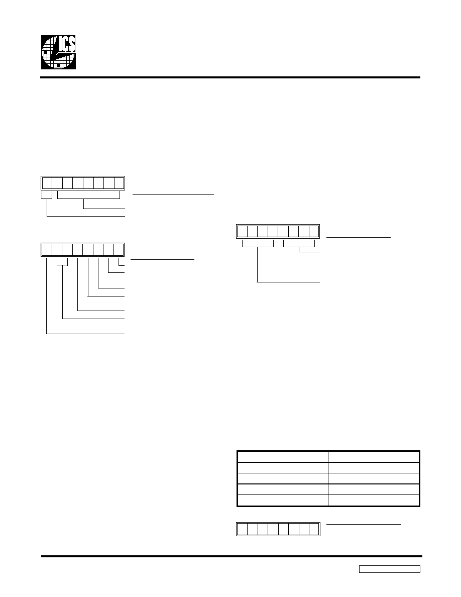
Fig. 4 - Crystal Oscillator
Fig. 5 ≠ Threshold Bias
Fig. 6 ≠ S-Video Input
Fig. 7 - Video Output
Fig. 8 - Self Biased Inputs

ICS2008B
16
ICS2008B Rev B 6/6/01
Programming
The ICS2008B is a SMPTE time code input/output device
with a UART which can be used as a MIDI UART or transport
control UART. All of the time critical functions to read and gen-
erate time code are performed by the chip's hardware, but all of
the intelligence for processing time codes and generating the
time code values are performed via an external processor. This
makes the ICS2008B flexible enough for a broad range of ap-
plications without making the processing requirements on the
host system too great.
Indirect Register Access
Indirect registers are accessed via the SMPTE2 (address) and
SMPTE3 (data) registers. To read an indirect register, the pro-
gram must first write its address to SMPTE2. Then the data is
read from SMPTE3. Writing to an indirect register is similar.
First, the address is written to SMPTE2. Then the data is writ-
ten to SMPTE3.
In order to minimize the number of accesses required to read
or write a block of registers, an auto-increment function is
provided. If the MSB of SMPTE2 is written to a one with the
address, the address is incremented after each read or write
access to SMPTE3. For example, if one wants to read the LTC
Read registers, IR0 to IR7, SMPTE2 is written to a 80h. Then
read SMPTE3 eight times. The first byte read is from IR0 fol-
lowed by IR1, etc.
Interrupt Processing
Interrupts can be generated from five sources, LTC receiver,
LTC generator, video line count, timer and UART. The inter-
rupt status of the first four interrupts, LRI, LXI, VLI and TMI
are in the SMPTE0 register. After this register is read, all four
interrupts are cleared. It is, therefore, necessary to save the
state of the interrupt status and process all active interrupts.
The UART interrupt status is in the UART0 register. The re-
ceive interrupt is cleared by reading the receive data register,
UART1. The transmit interrupt is cleared by writing data to
the transmit data register, UART1.
Reading LTC
When LTC data is received, it is placed into a temporary
buffer and transferred into the LTC read register (IR0 to IR7)
when the last bit of LTC data has been received. It should be
noted that the data is transferred before the SYNC pattern has
been received. Once the data is in the LTC receive buffer, the
LRI bit is set to one in the SMPTE0 register. If the LRIEN bit
(SMPTE0) is set to a one, an interrupt will be generated. The
interrupt is cleared when the SMPTE0 register is read. The
data in the LTC receive buffer remains valid until the next
LTC frame has been completely received.
LTC input data is available in the LTC Read registers after the
last LTC data bit has been received. It is not necessary to wait
for the LTC SYNC pattern to be complete. When LTC read
data is available the LRI bit in SMPTE0 is set to one. If
LRIEN is also set to one, an interrupt is generated. LRI and
the interrupt are cleared by reading SMPTE0. Data will re-
main valid until the last LTC data bit of the next frame has
been received.
The SMPTE1 register contains two status bits which indicate
whether LTC data is being received and if so which direction.
LTCLOCK is set to one when the LTC receiver has received a
valid LTC SYNC pattern and data is still coming in.
CODEDIR indicates the direction of the LTC SYNC pattern.
This is useful to tell whether a tape with LTC is shuttling for-
wards or backwards.
Generating LTC
The LTC generator transfers data from the LTC Write regis-
ters (IR8 to IRF) to the output buffer when the LTC generator
is enabled; LTCEN is set to one. Data transfers for subsequent
LTC frames occur eight bit times before the end of the LTC
frame being output. Remember that a LTC frame ends with a
16 bit SYNC pattern. The LXI interrupt bit in SMPTE0 is set
to one when LTC Write register data is transferred to the out-
put buffer.
A typical program for generating LTC output would first
setup the LTC control registers and the LTC bit time registers.
Then time code data would be written to the LTC Write regis-
ter. Once this setup is done the LTC output would be enabled
by setting LTCEN to a one. LTC output starts when a LTC
SYNC is received. The LTC SYNC source is selected as part
of the setup. While the LTC generator is waiting for SYNC,
the data in the LTC Write register is transferred to the output
buffer. When the transfer is complete the LXI status but is set
to a one. The data for the next LTC output frame can then be
loaded. The LXI status bit will be set to a one after the data
transfer at the end of the first LTC output frame. At this point
the LTC Write register is ready to receive data for a third LTC
output frame.

17
ICS2008B
ICS2008B Rev B 6/6/01
Reading VITC
To read VITC code one must first setup IR30 thru IR33. The
VITC Read Line registers, IR30 and IR31, select the video
line from which VITC code is to be read. The MSB is the en-
able for VITC reading. The Read Line field, bits 4 to 0, should
be programmed with the desired line number minus ten. So, if
line 15 is desired, a 5 should be programmed in the Read Line
field. If the read line field is set to 1Fh, this puts the VITC re-
ceiver into a scan mode. In scan mode, the VITC receiver
looks for a valid time code starting at line 10 for VITC1 or
VITC Read Line 1 for VITC2. The scan terminates when a
valid time code is received or the line count reads line 41.
IR32 selects the source and type of video. The GENLOCK
ENABLE bit must be set to a one, and the VTRES bit must be
set to a zero. The Video Interrupt Line register, IR33 should
be set to a line after all VITC read and write lines. This allows
all of the VITC receive and generate operations to be com-
plete before processing VITC.
The VLOCK bit in the SMPTE1 register indicates whether
the ICS2008B is genlocked to the selected video source.
Without the VLOCK status set to one, no VITC read will
occur.
When VLOCK is set to one and the control registers are prop-
erly initialized, VITC data are received a byte at a time from
the video signal and written to the VITC Read registers. At the
end of the VITC data frame the CRC byte is checked, and the
result reported in bit 5 of IR30 and IR31. In addition to the
CRC check, if a full VITC data frame is not received, the
NOCODE bit, bit 6, is set to a one.
Generating VITC
Like reading VITC, IR2E, IR2F, IR32 and IR33 must be setup
in order to generate VITC. The VITC Write Line registers,
IR2E and IR2F, select the video line to which VITC code is to
be written. The MSB is the enable for VITC generation. The
Write Line field, bits 4 to 0, should be programmed with the
desired line number minus ten. So, if line 12 is desired, a 2
should be programmed in the Write Line field. IR32 selects
the source and type of video. The GENLOCK ENABLE bit
must be set to a one, and the VTRES bit must be set to a zero.
The Video Interrupt Line register, IR33 should be set to a line
after all VITC read and write lines. This allows all of the
VITC receive and generate operations to be complete before
processing VITC.
With the VITC generator setup properly, when the selected
video line starts, the VITC data in the VITC Write buffer,
IR20 to IR27, is output. The video line interrupt, VLI in
SMPTE0, is provided to allow ample processing time for
VITC generation.
Burn-in Window
The burn-in window can be placed anywhere on the video
display. The position of the upper left corner of the window is
selected by the values written in IR28 and IR29. IR28 con-
trols the horizontal position. Values from 00h to 71h put the
corner in the first half of a video line (starting from the falling
edge of HSYNC). Values from 80h to F1h put the corner in
the second half of a video line. Any other values will not dis-
play the window. Care should be taken not to choose values
which put the window in any part of the blanking area. IR29
controls the vertical position. The value written here is the
video line number divided by 2.
IR3E controls the burn-in window character attributes. It con-
trols the size, normal and large, and the color of the characters
and background.
IR2A to IR2D, are the registers which control the characters
displayed in the burn-in window.
UART
The UART is accessed via two directly addressable registers,
the command/status register and the data register. On reset,
the UART is not operational. The command register must be
initialized before the UART will function.
Band rates are controlled in UART0 bits 1 and 0. 31.25 kHz
supports MIDI communications. 9600 Hz and 38.4 kHz sup-
port most serial VTR transport controls.
The UART has a four deep FIFO for its receive buffer. This
allows for relaxed interrupt latency requirements. In the case
of MIDI bit rates, the receiver will not overflow even if the
interrupt response delay is 1msec.
The UART's transmitter has a buffer in front of the output
shift register so that a byte can be loaded and waiting for the
output shifter to be empty.

ICS2008B
18
ICS2008B Rev B 6/6/01
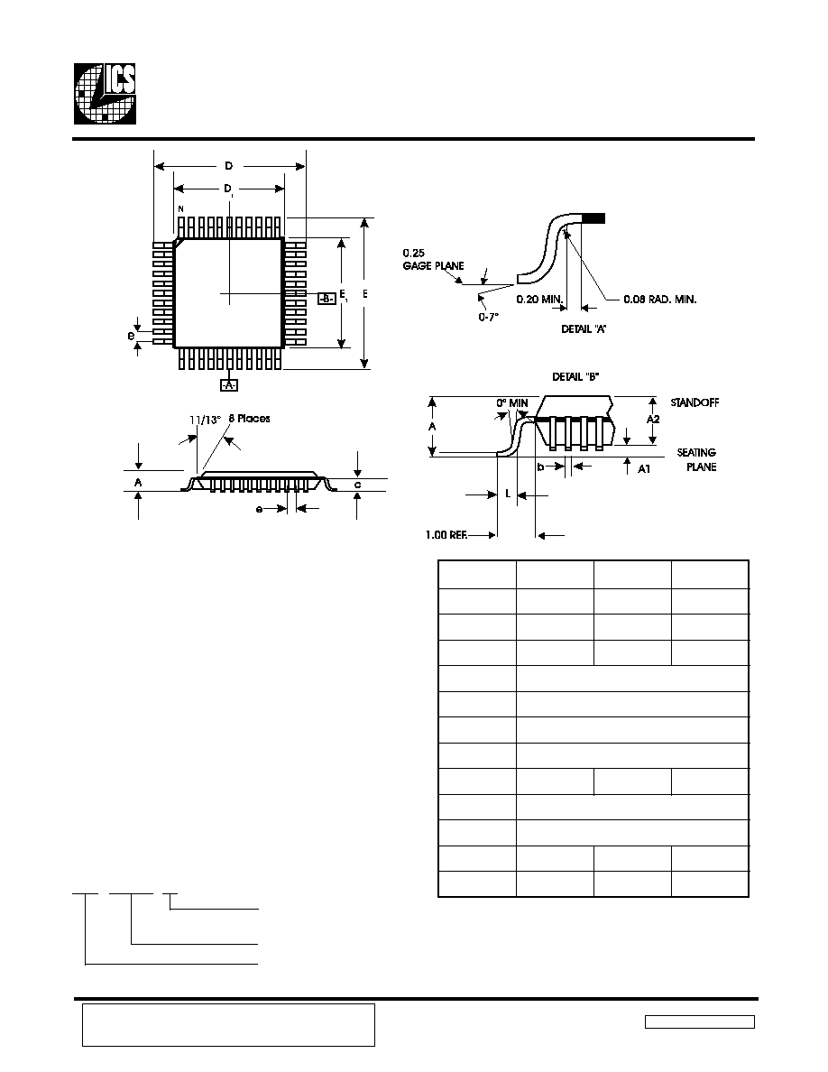
PLCC 44-PIN
PACKAGE
Ordering
Information
ICS2008BV
ICS 2008B X
Package Type
V = PLCC; Y-10 = 44 TQFP, EB = Evaluation Board
Device Type
Prefix
Example:
ICS reserves the right to make changes in the device data identified in
this publication without further notice. ICS advises its customers to
obtain the latest version of all device data to verify that any
information being relied upon by the customer is current and accurate.
19
ICS2008B
ICS2008B Rev B 6/6/01
Ordering
Information
ICS2008BY-10
ICS 2008B X
Package Type
Y-10 = 44 pin TQFP, V = 44 pin PLCC, EB = Evaluation Board
Device Type
Prefix
Example:
TQFP 44-PIN
PACKAGE
ICS reserves the right to make changes in the device data identified in
this publication without further notice. ICS advises its customers to
obtain the latest version of all device data to verify that any
information being relied upon by the customer is current and accurate.
l
o
b
m
y
S
N
I
M
M
R
O
N
X
A
M
A
-
-
0
2
.
1
A
1
5
0
.
0
0
1
.
0
5
1
.
0
A
2
5
9
.
0
0
0
.
1
5
0
.
1
D
.
C
S
B
0
0
.
2
1
D
1
.
C
S
B
0
0
.
0
1
E
.
C
S
B
0
0
.
2
1
E
1
.
C
S
B
0
0
.
0
1
L
5
4
.
0
0
6
.
0
5
7
.
0
N
4
4
e
.
C
S
B
0
8
.
0
b
0
3
.
0
7
3
.
0
5
4
.
0
c
-
-
0
1
.
0

ICS2008B
20
ICS2008B Rev B 6/6/01
Document Revision History
Rev A (First Release)
Started with ICS2008A Rev D Source Document
General cleanup for readability.
Rev B
Correct C2 pin number in Pin Description (pg 3)
Call out tieing LFC pin high in Pin Description (pg 3)
Added Document Revision History. (pg 20)
Added Corporate Contact Information (pg 21)

21
ICS2008B
ICS2008B Rev B 6/6/01
Corporate Headquarters:
2435 Boulevard of the Generals
P.O. Box 968
Valley Forge, PA 19482-0968
Telephone:
610-630-5300
Fax:
610-630-5399
San Jose Operations:
525 Race Street
San Jose, CA 95126-3448
Telephone:
408-297-1201
Fax:
408-925-9460
Web Site:
http://www.icst.com
Integrated Circuit Systems, Inc.