
ICS2059-02
MDS 2059-02 C
1
Revision 031605
Integrated Circuit Systems, Inc.
525 Race Street, San Jose, CA 95126
tel (408) 297-1201
www.icst.com
Clock Multiplier and Jitter Attenuator
Description
The ICS2059-02 is a VCXO (Voltage Controlled Crystal
Oscillator) based clock multiplier and jitter attenuator
designed for system clock distribution applications.
This monolithic IC, combined with an external
inexpensive quartz crystal, can be used to replace a
more costly hybrid VCXO retiming module. A dual input
mux is also provided.
By controlling the VCXO frequency within a
phase-locked loop (PLL), the output clock is phase and
frequency locked to the input clock. Through selection
of external loop filter components, the PLL loop
bandwidth and damping factor can be tailored to meet
system clock requirements. A loop bandwidth down to
the Hz range is possible.
Features
∑
Excellent jitter attenuation for telecom and video
clocks
∑
2:1 Input MUX for input reference clocks
∑
No switching glitches on output
∑
VCXO-based clock generation offers very low jitter
and phase noise generation
∑
Output clock is phase and frequency locked to the
selected input reference clock
∑
Fixed input to output phase relationship
∑
+115 ppm minimum crystal frequency pullability
range, using recommended crystal
∑
Industrial temperature range
∑
Low power CMOS technology
∑
16-pin TSSOP package
∑
Single 3.3 V power supply
Block Diagram
Charge
Pump
VCXO
Pullable Crystal
Selectable
Divider
Phase
Detector
ICLK1
Input Clock
ICLK2
Input Clock
ISEL
CLK
X2
X1
ISET
VDD
3
VDD
VIN
CHGP
2
GND
2
SEL1:0
0
1
Clock Multiplier and Jitter Attenuator
MDS 2059-02 C
2
Revision 031605
Integrated Circuit Systems, Inc.
525 Race Street, San Jose, CA 95126
tel (408) 297-1201
www.icst.com
ICS2059-02
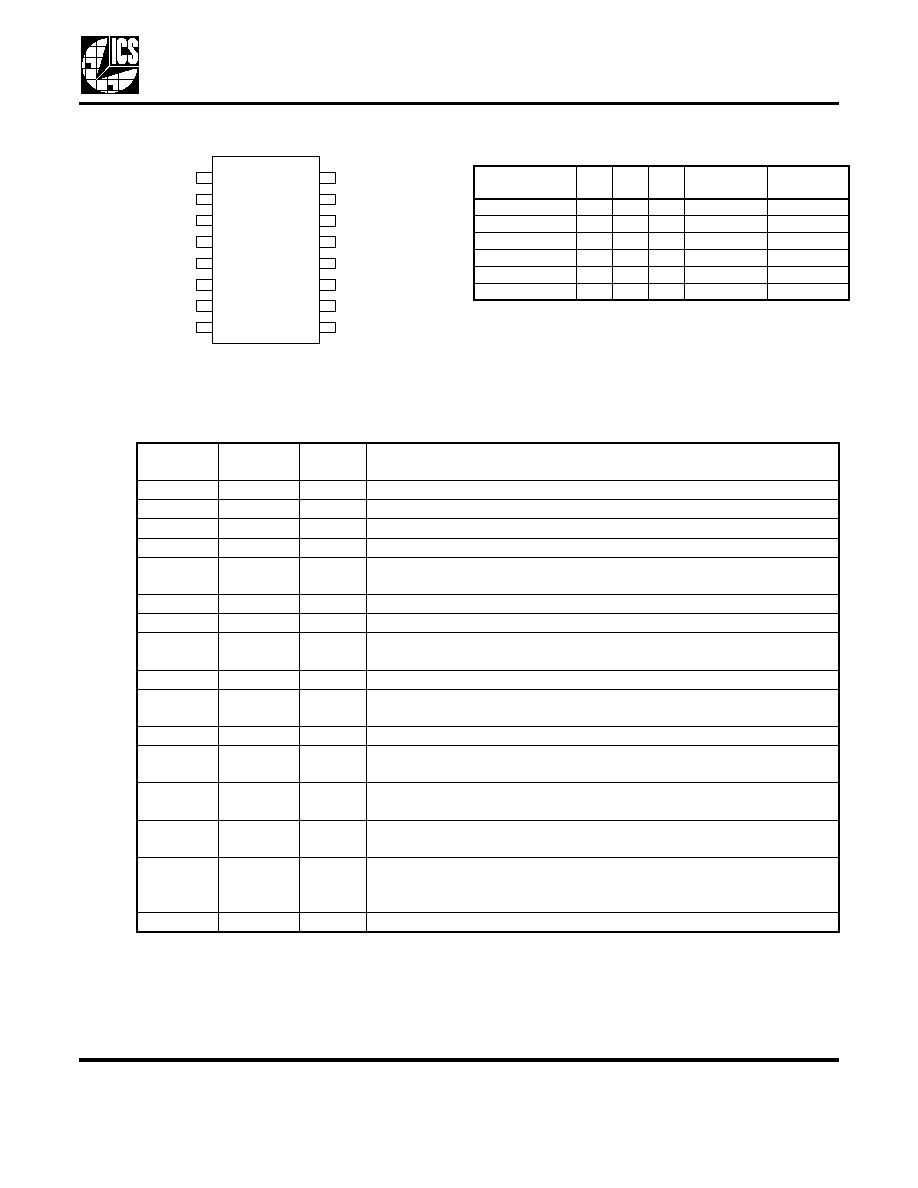
Pin Assignment
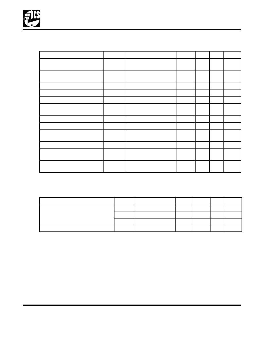
Output Frequency Select Table
Note: For SEL input pin programming:
0 = GND, 1 = VDD, M = Floating
Pin Descriptions
13
4
12
5
11
VIN
8
9
10
SEL0
ISET
16
3
VDD
VDD
ICLK2
ICLK1
1
X1
VDD
ISEL
X2
14
2
7
GND
SEL1
CLK
GND
15
6
16- pin ( 173 mil) TSSOP
CHGP
Input
SEL1 SEL0
N
Output Clock
(MHz)
Crystal Used
(MHz)
8 kHz
0
0
1296
10.368
20.736
8 kHz
0
1
2430
19.44
19.44
15.625 kHz
1
0
1728
27
27
15.734265 kHz
1
1
1716
27
27
151.875 kHz
M
0
128
19.44
19.44
27 MHz
M
1
1
27
27
Pin
Number
Pin
Name
Pin
Type
Pin Description
1
X1
--
Crystal Input. Connect this pin to the specified crystal.
2
VDD
Power
Power Supply. Connect to +3.3 V.
3
VDD
Power
Power Supply. Connect to +3.3 V.
4
VDD
Power
Power Supply. Connect to +3.3 V.
5
VIN
Input
VCXO Control Voltage Input. Connect this pin to CHGP pin and the
external loop filter as shown in this data sheet.
6
GND
Power
Connect to ground.
7
GND
Power
Connect to ground.
8
CHGP
Output
Charge Pump Output. Connect this pin to the external loop filter and to
pin VIN.
9
ISET
--
Charge pump current setting node, connection for setting resistor.
10
SEL1
Input
Output Frequency Selection Pin 1. Determines output frequency as
per table above. Includes mid-level input.
11
CLK
Output
Clock Output.
12
SEL0
Input
Output Frequency Selection Pin 0. Determines output frequency as
per table above. Internal pull-up resistor.
13
ICLK2
Input
Input Clock Connection 2. Connect an input reference clock to this pin.
If unused, connect to ground.
14
ICLK1
Input
Input Clock Connection 1. Connect an input reference clock to this pin.
If unused, connect to ground.
15
ISEL
Input
Input Selection. Used to select which reference input clock is active.
Low input level selects ICLK1, high input level selects ICLK2. Internal
pull-up resistor.
16
X2
--
Crystal Output. Connect this pin to the specified crystal.

Clock Multiplier and Jitter Attenuator
MDS 2059-02 C
3
Revision 031605
Integrated Circuit Systems, Inc.
525 Race Street, San Jose, CA 95126
tel (408) 297-1201
www.icst.com
ICS2059-02
Functional Description
The ICS2059-02 is a clock generator IC that generates
an output clock directly from an internal VCXO circuit
which works in conjunction with an external quartz
crystal. The VCXO is controlled by an internal PLL
(Phase-Locked Loop) circuit, enabling the device to
perform clock regeneration from an input reference
clock. The ICS2059-02 is configured to provide an
output clock that is the same frequency as the input
clock. There are 12 selectable input / output frequency
ranges, each of which is a submultiple of the supported
quartz crystal frequency range. Please refer to the
Output Clock Selection Table on Page 2.
Most typical PLL clock devices use an internal VCO
(Voltage Controlled Oscillator) for output clock
generation. By using a VCXO with an external crystal,
the ICS2059-02 is able to generate a low jitter, low
phase-noise output clock within a low bandwidth PLL.
This serves to provide input clock jitter attenuation and
enables stable operation with a low-frequency
reference clock.
The VCXO circuit requires an external pullable crystal
for operation. External loop filter components enable a
PLL configuration with low loop bandwidth.
Application Information
Input / Output Frequency Configuration
The ICS2059-02 is configured to generate an output
frequency that is equal to the input reference
frequency. Clock frequencies that are supported are
those which fall into the ranges listed in the Output
Clock Selection Table on Page 2. Input bits SEL2:0 are
set according to this table, as is the external crystal
frequency. Other input/output frequency combinations
can be used if the necessary integer multiplication
factor "N" appears in the Output Frequency Select
table. fro example, 20 MHz can be generated from
156.25 kHz by using select M0, as N=128.
Input Mux
The Input Mux serves to select between two alternate
input reference clocks. Upon reselection of the input
clock, clock glitches on the output clock will not be
generated due to the "fly-wheel" effect of the VCXO
(the quartz crystal is a high-Q tuned circuit). When the
input clocks are not phase aligned, the phase of the
output clock will change to reflect the phase of the
newly selected input at a controlled phase slope (rate
of phase change) as influenced by the PLL loop
characteristics.
Quartz Crystal
It is important that the correct type of quartz crystal is
used with the ICS2059-02. Failure to do so may result
in reduced frequency pullability range, inability of the
loop to lock, or excessive output phase jitter.
The ICS2059-02 operates by phase-locking the VCXO
circuit to the input signal of the selected ICLK input.
The VCXO consists of the external crystal and the
integrated VCXO oscillator circuit. To achieve the best
performance and reliability, a crystal device with the
recommended parameters (shown below) must be
used, and the layout guidelines discussed in the PCB
Layout Recommendations section must be followed.
The frequency of oscillation of a quartz crystal is
determined by its cut and by the external load
capacitance. The ICS2059-02 incorporates variable
load capacitors on-chip which "pull", or change, the
frequency of the crystal. The crystals specified for use
with the ICS2059-02 are designed to have zero
frequency error when the total of on-chip + stray
capacitance is 14 pF. To achieve this, the layout should
use short traces between the ICS2059-02 and the
crystal.
A complete description of the recommended crystal
parameters is in application note MAN05.
A list of approved crystals is located on the ICST web
site (
www.icst.com
).
PLL Loop Filter Components
All analog PLL circuits use a loop filter to establish
operating stability. The ICS2059-02 uses external loop
filter components for the following reasons:
1) Larger loop filter capacitor values can be used,
allowing a lower loop bandwidth. This enables the use
of lower input clock reference frequencies and also
input clock jitter attenuation capabilities. Larger loop
filter capacitors also allow higher loop damping factors
when less passband peaking is desired.
2) The loop filter values can be user selected to
optimize loop response characteristics for a given
application.

Clock Multiplier and Jitter Attenuator
MDS 2059-02 C
4
Revision 031605
Integrated Circuit Systems, Inc.
525 Race Street, San Jose, CA 95126
tel (408) 297-1201
www.icst.com
ICS2059-02
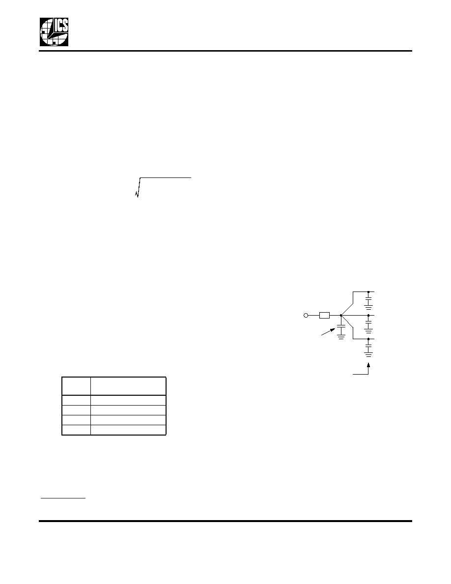
Referencing the External Component Schematic on
this page, the external loop filter is made up of the
components R
Z
, C
1
and C
2
. R
SET
establishes PLL
charge pump current and therefore influences loop
filter characteristics.
Design aid tools for configuring the loop filter can be
found at
www.icst.com
, including on-line and PC-based
calculators.
External Component Schematic
Recommended Loop Filter Values Vs. Output Frequency Range Selection
Note: For SEL input pin programming: 0 = GND, 1 = VDD, M = Floating
13
4
12
5
11
VIN
8
9
10
SEL0
ISET
16
3
VDD
VDD
ICLK2
ICLK1
1
VDD
ISEL
14
2
7
GND
SEL1
CLK
GND
15
6
16-pin (173 mil) TSSOP
CHGP
X1
X2
R
SET
C
L
C
L
Crystal
(Refer to Crystal
Tuning section)
C
S
R
S
P
SEL1 SEL0
Crystal
Multiplier
(N)
R
SET
R
S
C
S
C
P
Loop
Bandwidth
(-3dB point)
Damping
Factor
0
0
2592
180 k
820 k
0.47
µF
1.8 nF
11.2 Hz
3.00
0
1
2430
120 k
560 k
0.68
µF
3.3 nF
11.8 Hz
2.97
1
0
1728
330 k
680 k
0.68
µF
3.9 nF
11.5 Hz
3.17
1
1
1716
330 k
680 k
0.68
µF
3.9 nF
11.5 Hz
3.18
M
0
128
120 k
330 k
1
µF
3.3 nF
14.5 Hz
3.16
M
1
1
1 M
22 k
1
µF
3.3 nF
204.2 Hz
3.08
Clock Multiplier and Jitter Attenuator
MDS 2059-02 C
5
Revision 031605
Integrated Circuit Systems, Inc.
525 Race Street, San Jose, CA 95126
tel (408) 297-1201
www.icst.com
ICS2059-02
A "normalized" PLL loop bandwidth may be calculated
as follows:
The "normalized" bandwidth equation above does not
take into account the effects of damping factor or the
second pole. However, it does provide a useful
approximation of filter performance.
The loop damping factor is calculated as follows:
Where:
R
S
= Value of resistor in loop filter (Ohms)
I
CP
= Charge pump current (amps)
(refer to Charge Pump Current Table, below)
N = Crystal multiplier shown in the above table
C
S
= Value of capacitor C
1
in loop filter (Farads)
As a general rule, the following relationship should be
maintained between components C
1
and C
2
in the loop
filter:
Charge Pump Current Table
Special considerations must be made in choosing loop
components C
S
and C
P.
These recommendations can
be found in the design aid tools section of
www.icst.com
.
Series Termination Resistor
Clock output traces over one inch should use series
termination. To series terminate a 50
trace (a
commonly used trace impedance), place a 33
resistor
in series with the clock line, as close to the clock output
pin as possible. The nominal impedance of the clock
output is 20
. (The optional series termination resistor
is not shown in the External Component Schematic.)
Decoupling Capacitors
As with any high-performance mixed-signal IC, the
ICS2059-02 must be isolated from system power
supply noise to perform optimally.
Decoupling capacitors of 0.01µF must be connected
between each VDD and the PCB ground plane. To
further guard against interfering system supply noise,
the ICS2059-02 should use one common connection to
the PCB power plane as shown in the diagram on the
next page. The ferrite bead and bulk capacitor help
reduce lower frequency noise in the supply that can
lead to output clock phase modulation.
Recommended Power Supply Connection
for Optimal Device Performance
Crystal Load Capacitors
The device crystal connections should include pads for
small capacitors from X1 to ground and from X2 to
ground, shown as C
L
in the External Component
Schematic. These capacitors are used to adjust the
stray capacitance of the board to match the nominally
required crystal load capacitance. Because load
capacitance can only be increased in this trimming
process, it is important to keep stray capacitance to a
minimum by using very short PCB traces (and no vias)
been the crystal and device.
R
SET
Charge Pump Current
(I
CP
)
1.4 M
10
µA
680 k
20
µA
540 k
25
µA
120 k
100
µA
NBW
R
S
I
CP
◊
575
◊
N
---------------------------------------
=
345
Damping Factor
R
S
625
I
CP
◊
C
S
◊
N
-----------------------------------------
◊
=
375
C
P
C
S
20
------
=
C onnec tion to 3.3V
P ow er P lane
Ferrite
B ead
B ulk D ec oupling C apac itor
(suc h as 1
F Tantalum )
V D D P in
V D D P in
V D D P in
0.01
F D ecoupling C apacitors

Clock Multiplier and Jitter Attenuator
MDS 2059-02 C
6
Revision 031605
Integrated Circuit Systems, Inc.
525 Race Street, San Jose, CA 95126
tel (408) 297-1201
www.icst.com
ICS2059-02
In most cases the load capacitors will not be required.
They should not be stuffed on the prototype evaluation
board as the indiscriminate use of these trim capacitors
will typically cause more crystal centering error than
their absence. If the need for the load capacitors is later
determined, the values will fall within the 1-4 pf range.
The need for, and value of, these trim capacitors can
only be determined at prototype evaluation. Please
refer to MAN05 for the procedure to determine the
component values.
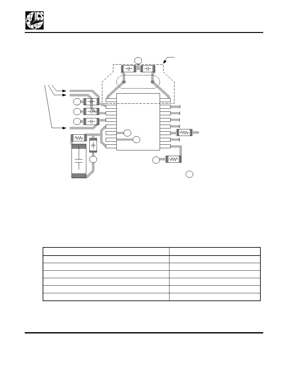
PCB Layout Recommendations
For optimum device performance and lowest output
phase noise, the following guidelines should be
observed. Please also refer to the Recommended PCB
Layout drawing on page 7.
1) Each 0.01µF decoupling capacitor should be
mounted on the component side of the board as close
to the VDD pin as possible. No vias should be used
between decoupling capacitor and VDD pin. The PCB
trace to VDD pin should be kept as short as possible,
as should the PCB trace to the ground via. Distance of
the ferrite bead and bulk decoupling from the device is
less critical.
2) The loop filter components must also be placed
close to the CHGP and VIN pins. C
P
should be closest
to the device. Coupling of noise from other system
signal traces should be minimized by keeping traces
short and away from active signal traces. Use of vias
should be avoided.
3) The external crystal should be mounted just next to
the device with short traces. The X1 and X2 traces
should not be routed next to each other with minimum
spaces, instead they should be separated and away
from other traces.
4) To minimize EMI, the 33
series termination resistor
(if needed) should be placed close to the clock output.
5) An optimum layout is one with all components on the
same side of the board, minimizing vias through other
signal layers (the ferrite bead and bulk decoupling
capacitor can be mounted on the back). Other signal
traces should be routed away from the ICS2059-02.
This includes signal traces just underneath the device,
or on layers adjacent to the ground plane layer used by
the device.
The ICS Applications Note MAN05 may also be
referenced for additional suggestions on layout of the
crystal section.
Clock Multiplier and Jitter Attenuator
MDS 2059-02 C
7
Revision 031605
Integrated Circuit Systems, Inc.
525 Race Street, San Jose, CA 95126
tel (408) 297-1201
www.icst.com
ICS2059-02
Recommended PCB Layout
Absolute Maximum Ratings
Stresses above the ratings listed below can cause permanent damage to the ICS2059-02. These ratings,
which are standard values for ICS commercially rated parts, are stress ratings only. Functional operation of
the device at these or any other conditions above those indicated in the operational sections of the
specifications is not implied. Exposure to absolute maximum rating conditions for extended periods can
affect product reliability. Electrical parameters are guaranteed only over the recommended operating
temperature range.
Item
Rating
Supply Voltage, VDD
7 V
All Inputs and Outputs
-0.5 V to VDD+0.5 V
Ambient Operating Temperature
-40 to +85
∞C
Storage Temperature
-65 to +150
∞C
Junction Temperature
125
∞C
Soldering Temperature
260
∞C
remove ground and power plane
within this entire area. Also route
all other traces away from this area.
12
11
10
9
16
15
14
13
1
2
3
4
5
6
7
G
For minimum output clock jitter,
= Ground
Connection
G
G
G
G
G
G
G
G
Legend:
For minimum output clock jitter,
device VDD connections should
be made to common bulk
decoupling device (see text).
8
Clock Multiplier and Jitter Attenuator
MDS 2059-02 C
8
Revision 031605
Integrated Circuit Systems, Inc.
525 Race Street, San Jose, CA 95126
tel (408) 297-1201
www.icst.com
ICS2059-02
Recommended Operation Conditions
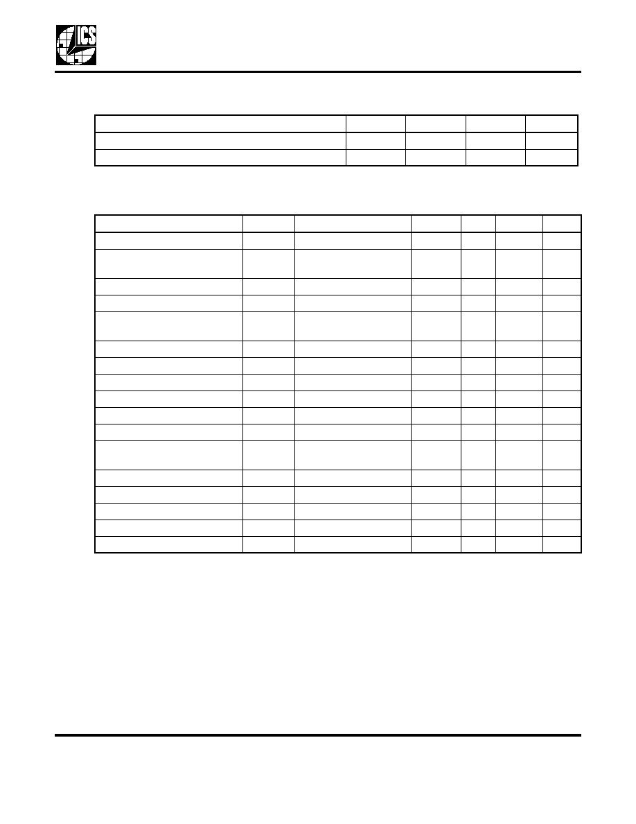
DC Electrical Characteristics
Unless stated otherwise, VDD = 3.3 V ±5%, Ambient Temperature -40 to +85
∞C
Parameter
Min.
Typ.
Max.
Units
Ambient Operating Temperature
-40
+85
∞C
Power Supply Voltage (measured in respect to GND)
+3.15
+3.3
+3.45
V
Parameter
Symbol
Conditions
Min.
Typ.
Max.
Units
Operating Voltage
VDD
3.15
3.3
3.45
V
Supply Current
IDD
Clock outputs
unloaded, VDD = 3.3 V
10
15
mA
Input High Voltage, SEL1
V
IH
VDD-0.5
V
Input Low Voltage, SEL1
V
IL
0.5
V
Input High Voltage, ISEL,
SEL0
V
IH
2
V
Input Low Voltage, ISEL, SEL0
V
IL
0.8
V
Input High Voltage, ICLK1, 2
V
IH
VDD/2+1
V
Input Low Voltage, ICLK1, 2
V
IL
VDD/2-1
V
Input High Current
I
IH
V
IH
= VDD
-10
+10
µA
Input Low Current
I
IL
V
IL
= 0
-10
+10
µA
Input Capacitance, except X1
C
IN
7
pF
Output High Voltage (CMOS
Level)
V
OH
I
OH
= -4 mA
VDD-0.4
V
Output High Voltage
V
OH
I
OH
= -8 mA
2.4
V
Output Low Voltage
V
OL
I
OL
= 8 mA
0.4
V
Short Circuit Current
I
OS
±50
mA
VIN, VCXO Control Voltage
V
XC
0
VDD
V
Nominal Output Impedance
Z
OUT
20
Clock Multiplier and Jitter Attenuator
MDS 2059-02 C
9
Revision 031605
Integrated Circuit Systems, Inc.
525 Race Street, San Jose, CA 95126
tel (408) 297-1201
www.icst.com
ICS2059-02
AC Electrical Characteristics
Unless stated otherwise, VDD = 3.3 V ±5%, Ambient Temperature -40 to +85
∞ C
Note 1: Minimum high or low time of input clock.
Thermal Characteristics
Parameter
Symbol
Conditions
Min.
Typ. Max.
Units
VCXO Crystal Pull Range
f
XP
Using recommended
crystal
-115
+115
ppm
VCXO Crystal Nominal
Frequency
f
X
8.5
27
MHz
Input Jitter Tolerance
t
ji
0.4
UI
Input pulse width (1)
t
pi
10
ns
Output Frequency Error
F
OUT
ICLK = 0 ppm error
0
0
0
ppm
Output Duty Cycle
(% high time)
t
OD
Measured at VDD/2,
C
L
=15 pF
40
60
%
Output Rise Time
t
OR
0.8 to 2.0V , C
L
=15 pF
1.5
ns
Output Fall Time
t
OF
2.0 to 0.8 V, C
L
=15 pF
1.5
ns
Skew, Input to Output Clock
t
IO
27 MHz output, rising
edges, C
L
=15 pF
-5
+5
ns
Cycle Jitter (short term jitter)
t
ja
150
ps
p-p
Timing Jitter, Filtered
500 Hz-1.3 MHz (OC-3)
t
jf
210
ps p-p
Timing Jitter, Filtered
65 kHz-1.3 MHz (OC-3)
t
jf
150
ps p-p
Parameter
Symbol
Conditions
Min.
Typ.
Max.
Units
Thermal Resistance Junction to
Ambient
JA
Still air
78
∞C/W
JA
1 m/s air flow
70
∞C/W
JA
3 m/s air flow
68
∞C/W
Thermal Resistance Junction to Case
JC
37
∞C/W
Clock Multiplier and Jitter Attenuator
MDS 2059-02 C
10
Revision 031605
Integrated Circuit Systems, Inc.
525 Race Street, San Jose, CA 95126
tel (408) 297-1201
www.icst.com
ICS2059-02
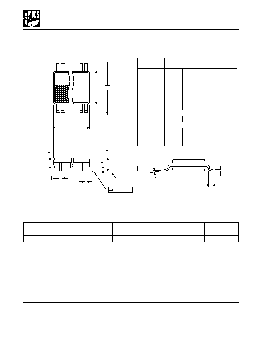
Package Outline and Package Dimensions
(16-pin TSSOP, 173 Mil. Narrow Body)
Package dimensions are kept current with JEDEC Publication No. 95
Ordering Information
While the information presented herein has been checked for both accuracy and reliability, Integrated Circuit Systems (ICS)
assumes no responsibility for either its use or for the infringement of any patents or other rights of third parties, which would
result from its use. No other circuits, patents, or licenses are implied. This product is intended for use in normal commercial
applications. Any other applications such as those requiring extended temperature range, high reliability, or other extraordinary
environmental requirements are not recommended without additional processing by ICS. ICS reserves the right to change any
circuitry or specifications without notice. ICS does not authorize or warrant any ICS product for use in life support devices or
critical medical instruments.
Part / Order Number
Marking
Shipping Packaging
Package
Temperature
ICS2059GI-02
2059GI02
Tubes
16-pin TSSOP
-40 to +85
∞ C
ICS2059GI-02T
2059GI02
Tape and Reel
16-pin TSSOP
-40 to +85
∞ C
IN D E X
A R E A
1 2
16
D
E 1
E
S E A TIN G
P LA N E
A
1
A
A
2
e
- C -
b
aaa
C
c
L
Millimeters
Inches
Symbol
Min
Max
Min
Max
A
--
1.20
--
0.047
A1
0.05
0.15
0.002
0.006
A2
0.80
1.05
0.032
0.041
b
0.19
0.30
0.007
0.012
C
0.09
0.20
0.0035
0.008
D
4.90
5.1
0.193
0.201
E
6.40 BASIC
0.252 BASIC
E1
4.30
4.50
0.169
0.177
e
0.65 Basic
0.0256 Basic
L
0.45
0.75
0.018
0.030
0
∞
8
∞
0
∞
8
∞
aaa
--
0.10
--
0.004
Clock Multiplier and Jitter Attenuator
MDS 2059-02 C
11
Revision 031605
Integrated Circuit Systems, Inc.
525 Race Street, San Jose, CA 95126
tel (408) 297-1201
www.icst.com
ICS2059-02
Revision History
Rev.
Originator
Date
Description of Change
A
P.Griffith
11/19/04
New device/datasheet. Change proposal number from 4MPG019 to ICS2059-02. Move
from Advance to Preliminary.
B
P.Griffith
11/29/04
Updated values for "Loop Bandwidth" and" Damping Factor" in "Recommended Loop
Filter Values vs Output Frequency Range Selection" table;
C
P.Griffith
03/16/05
Released to Final and standard, general purpose device.