ICS2309
MDS 2309 D
1
Revision 052405
I n t e gra t e d C i r c u i t S y s t e m s
5 2 5 R a c e S t r e e t , S a n J o s e, C A 9 5 1 2 6
t e l ( 4 0 8 ) 2 9 7 - 1 2 0 1
w w w. i c s t . c o m
3.3 V
OLT
Z
ERO
D
ELAY
, L
OW
S
KEW
B
UFFER
Description
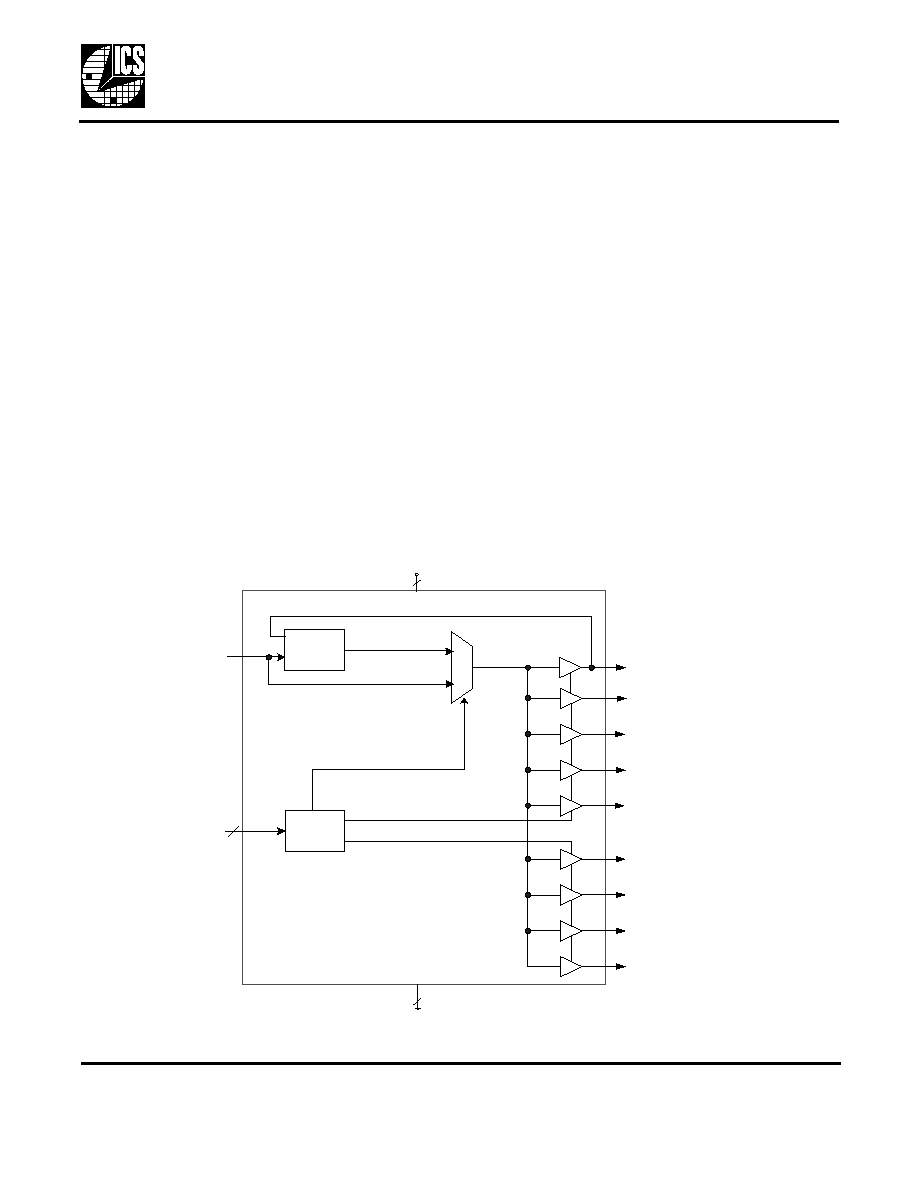
The ICS2309 is a low phase noise, high-speed PLL
based, low-skew zero delay buffer. Based on ICS'
proprietary low jitter Phase Locked Loop (PLL)
techniques, the device provides eight low skew outputs
at speeds up to 133 MHz at 3.3 V. The outputs can be
generated from the PLL (for zero delay), or directly
from the input (for testing), and can be set to tri-state
mode or to stop at a low level. The PLL feedback is
on-chip and is obtained from the CLKOUT pad.
The ICS2309 is available in two different versions. The
ICS2309-1 is the base part. The ICS2309-1H is a high
drive version with faster rise and fall times.
Features
�
Clock outputs from 10 to 133 MHz
�
Zero input-output delay
�
Eight low skew (<250 ps) outputs
�
Device-to-device skew <700 ps
�
Full CMOS outputs with 25 mA output drive
capability at TTL levels
�
5 V tolerant CLKIN
�
Tri-state mode for board-level testing
�
Advanced, low power, sub-micron CMOS process
�
Operating voltage of 3.3 V
�
Industrial temperature range available
�
Packaged in 16-pin SOIC and TSSOP (-1H version
only)
�
Pb (lead) free package available for -1H version
(16-pin TSSOP only)
Block Diagram
CLKA4
CLKB1
CLKA3
CLKB2
CLKB3
CLKA2
CLKA1
CLKB4
CLKIN
Control
Logic
1
0
S2, S1 2
PLL
VDD
2
GND
2
CLKOUT
3.3 V
OLT
Z
ERO
D
ELAY
, L
OW
S
KEW
B
UFFER
MDS 2309 D
2
Revision 052405
I n t e gr a t e d C i r c u i t S y s t e m s
5 2 5 R a c e S t r e e t , S a n J o s e, C A 9 5 1 2 6
t e l ( 4 0 8 ) 2 9 7 - 1 2 0 1
w w w. i c s t . c o m
ICS2309
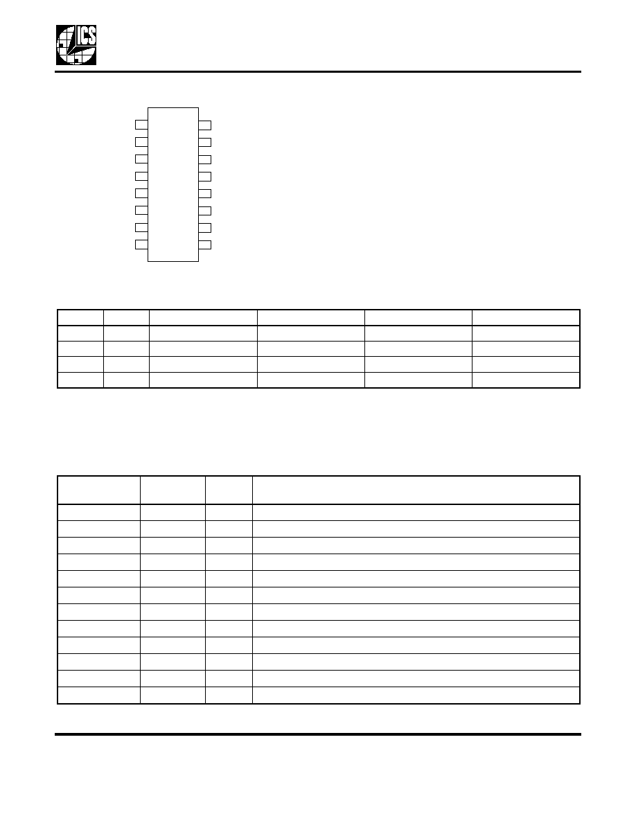
Pin Assignment
Output Clock Mode Select Table
Note 1. Outputs are in high impedance state
Note 2. Buffer mode only; not zero delay between input and output
Pin Descriptions
12
1
11
2
10
CLKIN
CLKOUT
3
9
CLKA1
4
CLKA2
CLKA4
5
VDD
6
CLKA3
7
GND
8
CLKB1
VDD
GND
CLKB4
CLKB2
CLKB3
S2
S1
16
15
14
13
16 pin narrow (150 mil) SOIC
S2
S1
CLKA1:A4
CLKB1:B4
A & B Source
PLL Status
0
0
Tri-state (note 1)
Tri-state (note 1)
PLL
OFF
0
1
Running
Tri-state (note 1)
PLL
ON
1
0
Running
Running
CLKIN (note 2)
OFF
1
1
Running
Running
PLL
ON
Pin
Number
Pin
Name
Pin Type
Pin Description
1
CLKIN
Input
Clock input (5 V tolerant).
2 - 3
CLKA1:A4
Output
Clock outputs A1:A4. See table above.
4
VDD
Power
Power supply. Connect to 3.3 V.
5
GND
Power
Connect to ground.
6 - 7
CLKB1:B4
Output
Clock outputs B1:B4. See table above.
8
S2
Input
Select input 2. See table above. Internal pull-up.
9
S1
Input
Select input 1. See table above. Internal pull-up.
10 - 11
CLKB1:B4
Output
Clock outputs B1:B4. See table above.
12
GND
Power
Connect to ground.
13
VDD
Power
Power supply. Connect to 3.3 V.
14 - 15
CLKA1:A4
Output
Clock outputs A1:A4. See table above.
16
CLKOUT
Input
Buffered output. Internall feedback on this pin.
3.3 V
OLT
Z
ERO
D
ELAY
, L
OW
S
KEW
B
UFFER
MDS 2309 D
3
Revision 052405
I n t e gr a t e d C i r c u i t S y s t e m s
5 2 5 R a c e S t r e e t , S a n J o s e, C A 9 5 1 2 6
t e l ( 4 0 8 ) 2 9 7 - 1 2 0 1
w w w. i c s t . c o m
ICS2309
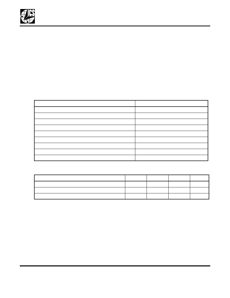
External Components
The ICS2309 requires a minimum number of external components for proper operation. Decoupling
capacitors of 0.01 mF should be connected between VDD and GND on pins 4 and 5, and VDD and GND
on pins 13 and 12, as close to the device as possible. A series termination resistor of 33
may be used to
each clock output pin to reduce reflections.
Absolute Maximum Ratings
Stresses above the ratings listed below can cause permanent damage to the ICS2309. These ratings,
which are standard values for ICS commercially rated parts, are stress ratings only. Functional operation of
the device at these or any other conditions above those indicated in the operational sections of the
specifications is not implied. Exposure to absolute maximum rating conditions for extended periods can
affect product reliability. Electrical parameters are guaranteed only over the recommended operating
temperature range.
Recommended Operation Conditions
Item
Rating
Supply Voltage, VDD
7 V
All Inputs and Outputs
-0.5 V to VDD+0.5 V
CLKIN and FBIN inputs
-0.5 V to 5.5 V
Electrostatic Discharge (HBM)
2000 V
Ambient Operating Temperature (Commercial)
0 to +70
�C
Ambient Operating Temperature (Industrial)
-40 to +85
�C
Storage Temperature
-65 to +150
�C
Junction Temperature
150
�C
Soldering Temperature
260
�C
Parameter
Min.
Typ.
Max.
Units
Ambient Operating Temperature (Industrial)
-40
+85
�C
Ambient Operating Temperature (Commercial)
0
+70
�C
Power Supply Voltage (measured in respect to GND)
+3.0
+3.6
V

3.3 V
OLT
Z
ERO
D
ELAY
, L
OW
S
KEW
B
UFFER
MDS 2309 D
4
Revision 052405
I n t e gr a t e d C i r c u i t S y s t e m s
5 2 5 R a c e S t r e e t , S a n J o s e, C A 9 5 1 2 6
t e l ( 4 0 8 ) 2 9 7 - 1 2 0 1
w w w. i c s t . c o m
ICS2309
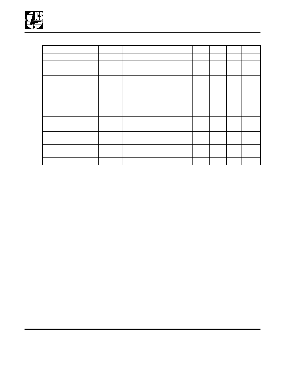
DC Electrical Characteristics
ICS2309M-1, VDD = 3.3 V �10%, Ambient Temperature -40 to +85
�C(Industrial), (0-70�C Commercial)
Note 1: When there is no clock signal present at CLKIN, the ICS2309 will enter power down mode. The
PLL is stopped and the outputs are tri-state.
AC Electrical Characteristics
ICS2309M-1, VDD=3.3 V �10%,
Ambient temperature -40 to +85
�C(Industrial), (0-70�C Commercial),
Note 2: With VDD at a steady rate and valid input at CLKIN
Parameter
Symbol
Conditions
Min.
Typ.
Max.
Units
Operating Voltage
VDD
3.0
3.6
V
Input High Voltage
V
IH
2
V
Input Low Voltage
V
IL
0.8
V
Input Low Current
I
IL
VIN = 0V
50
�A
Input High Current
I
IH
VIN = VDD
100
�A
Output High Voltage
V
OH
I
OH
= -12 mA
2.4
V
Output Low Voltage
V
OL
I
OL
= 12 mA
0.4
V
Operating Supply Current
IDD
No Load
32
mA
Power Down Supply
Current
CLKIN = 0, Note 1
12
�A
Short Circuit Current
I
OS
Each output
�50
mA
Input Capacitance
C
IN
S2, S1, CLKIN
5
pF
Parameter
Symbol
Conditions
Min.
Typ. Max. Units
Output Clock Frequency
f
IN
10 pF load, See table on page 2
10
133
MHz
Output Clock Frequency
30 pF load, See table on page 2
10
100
MHz
Output Rise Time
t
OR
0.8 to 2.0 V, outputs loaded
2.5
ns
Output Fall Time
t
OF
2.0 to 0.8 V, outputs loaded
2.5
ns
Output Clock Duty Cycle
t
DC
measured at 1.4V, Fout=66.67
MHz
40
50
60
%
Output Clock Duty Cycle
t
DC
measured at 1.4V, Fout=50
MHz
45
50
55
%
Device to Device Skew
rising edges at VDD/2
700
ps
Output to Output Skew
rising edges at VDD/2
250
ps
Input to Output Skew
rising edges at VDD/2
�350
ns
Input to Output Skew
rising edges at VDD/2, S2= 1,
S1 = 0
1
5
8.7
ns
Cycle to Cycle Jitter
measured at 66.67M, outputs
loaded
200
ps
PLL Lock Time
Note 2
1.0
ms
3.3 V
OLT
Z
ERO
D
ELAY
, L
OW
S
KEW
B
UFFER
MDS 2309 D
5
Revision 052405
I n t e gr a t e d C i r c u i t S y s t e m s
5 2 5 R a c e S t r e e t , S a n J o s e, C A 9 5 1 2 6
t e l ( 4 0 8 ) 2 9 7 - 1 2 0 1
w w w. i c s t . c o m
ICS2309
ICS2309M-1H, VDD=3.3 V �10%,
Ambient temperature -40 to +85
�C(Industrial), (0-70�C Commercial),
Note 3: With VDD at a steady rate and valid input at CLKIN
Parameter
Symbol
Conditions
Min.
Typ. Max. Units
Output Clock Frequency
f
IN
10 pF load, See table on page 2
10
133
MHz
Output Clock Frequency
30 pF load, See table on page 2
10
100
MHz
Output Rise Time
t
OR
0.8 to 2.0 V, outputs loaded
1.5
ns
Output Fall Time
t
OF
2.0 to 0.8 V, outputs loaded
1.5
ns
Output Clock Duty Cycle
t
DC
measured at 1.4V, Fout=66.67
MHz
40
50
60
%
Output Clock Duty Cycle
t
DC
measured at 1.4V, Fout=50
MHz
45
50
55
%
Device to Device Skew
rising edges at VDD/2
700
ps
Output to Output Skew
rising edges at VDD/2
250
ps
Input to Output Skew
rising edges at VDD/2
�350
ps
Input to Output Skew
rising edges at VDD/2, S2= 1,
S1 = 0
1
5
8.7
ns
Cycle to Cycle Jitter
measured at 66.67M, outputs
loaded
200
ps
PLL Lock Time
Note 3
1.0
ms
3.3 V
OLT
Z
ERO
D
ELAY
, L
OW
S
KEW
B
UFFER
MDS 2309 D
6
Revision 052405
I n t e gr a t e d C i r c u i t S y s t e m s
5 2 5 R a c e S t r e e t , S a n J o s e, C A 9 5 1 2 6
t e l ( 4 0 8 ) 2 9 7 - 1 2 0 1
w w w. i c s t . c o m
ICS2309
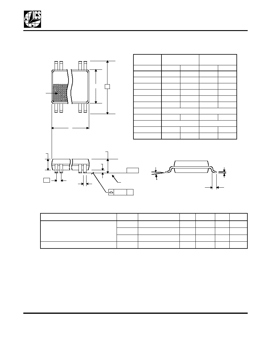
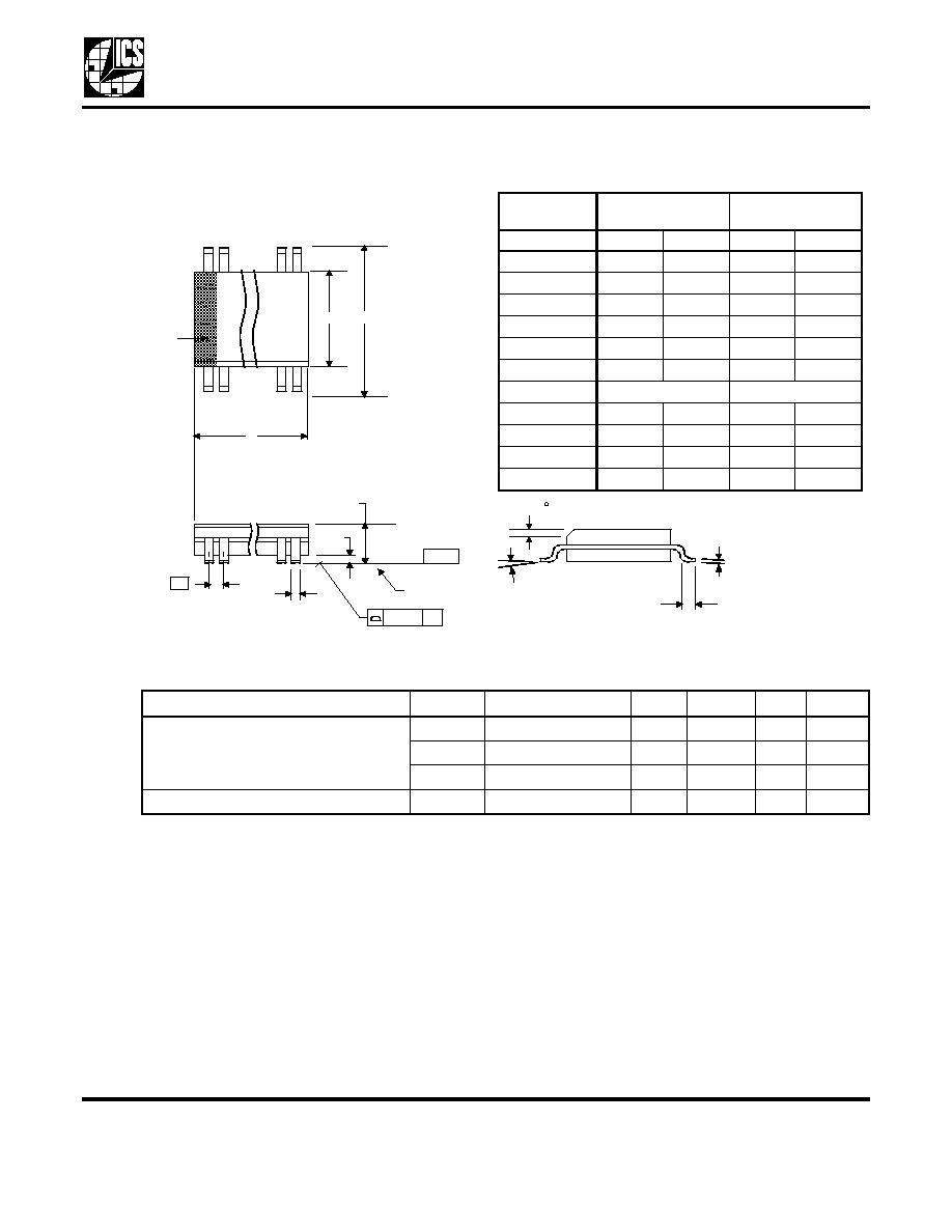
Package Outline and Package Dimensions (
16-pin TSSOP,
4.40 mm Body, 0.65 mm Pitch
)
Package dimensions are kept current with JEDEC Publication No. 95
Thermal Characteristics for 16TSSOP
Parameter
Symbol
Conditions
Min.
Typ.
Max.
Units
Thermal Resistance Junction to
Ambient
JA
Still air
78
�C/W
JA
1 m/s air flow
70
�C/W
JA
3 m/s air flow
68
�C/W
Thermal Resistance Junction to Case
JC
37
�C/W
INDEX
AREA
1 2
16
D
E1
E
SEATING
PLANE
A
1
A
A
2
e
- C -
b
.10 (.004)
C
c
L
Millimeters
Inches
Symbol
Min
Max
Min
Max
A
--
1.20
--
0.047
A1
0.05
0.15
0.002
0.006
A2
0.80
1.05
0.032
0.041
b
0.19
0.30
0.007
0.012
C
0.09
0.20
0.0035
0.008
D
4.90
5.1
0.193
0.201
E
6.40 BASIC
0.252 BASIC
E1
4.30
4.50
0.169
0.177
e
0.65 Basic
0.0256 Basic
L
0.45
0.75
0.018
0.030
0
�
8
�
0
�
8
�
3.3 V
OLT
Z
ERO
D
ELAY
, L
OW
S
KEW
B
UFFER
MDS 2309 D
7
Revision 052405
I n t e gr a t e d C i r c u i t S y s t e m s
5 2 5 R a c e S t r e e t , S a n J o s e, C A 9 5 1 2 6
t e l ( 4 0 8 ) 2 9 7 - 1 2 0 1
w w w. i c s t . c o m
ICS2309
Package Outline and Package Dimensions
(16-pin SOIC, 150 Mil. Narrow Body)
Package dimensions are kept current with JEDEC Publication No. 95
Thermal Characteristics for 16SOIC
Parameter
Symbol
Conditions
Min.
Typ.
Max.
Units
Thermal Resistance Junction to
Ambient
JA
Still air
120
�C/W
JA
1 m/s air flow
115
�C/W
JA
3 m/s air flow
105
�C/W
Thermal Resistance Junction to Case
JC
58
�C/W
INDEX
AREA
1 2
16
D
E
SEATING
PLANE
A1
A
e
- C -
B
.10 (.004)
C
C
L
H
h x 45
Millimeters
Inches
Symbol
Min
Max
Min
Max
A
1.35
1.75
.0532
.0688
A1
0.10
0.25
.0040
.0098
B
0.33
0.51
.013
.020
C
0.19
0.25
.0075
.0098
D
9.80
10.00
.3859
.3937
E
3.80
4.00
.1497
.1574
e
1.27 BASIC
0.050 BASIC
H
5.80
6.20
.2284
.2440
h
0.25
0.50
.010
.020
L
0.40
1.27
.016
.050
0
�
8
�
0
�
8
�

3.3 V
OLT
Z
ERO
D
ELAY
, L
OW
S
KEW
B
UFFER
MDS 2309 D
8
Revision 052405
I n t e gr a t e d C i r c u i t S y s t e m s
5 2 5 R a c e S t r e e t , S a n J o s e, C A 9 5 1 2 6
t e l ( 4 0 8 ) 2 9 7 - 1 2 0 1
w w w. i c s t . c o m
ICS2309
Ordering Information
Parts that are ordered with a "LF" suffix to the part number are the Pb-Free configuration and are RoHS compliant.
While the information presented herein has been checked for both accuracy and reliability, Integrated Circuit Systems (ICS) assumes no
responsibility for either its use or for the infringement of any patents or other rights of third parties, which would result from its use. No other
circuits, patents, or licenses are implied. This product is intended for use in normal commercial applications. Any other applications such as
those requiring extended temperature range, high reliability, or other extraordinary environmental requirements are not recommended without
additional processing by ICS. ICS reserves the right to change any circuitry or specifications without notice. ICS does not authorize or warrant
any ICS product for use in life support devices or critical medical instruments.
Part / Order Number
Marking
Shipping Packaging
Package
Temperature
ICS2309MI-1
ICS2309MI-1
Tubes
16-pin SOIC
-40 to +85
� C
ICS2309MI-1T
ICS2309MI-1
Tape and Reel
16-pin SOIC
-40 to +85
� C
ICS2309M-1
ICS2309M-1
Tubes
16-pin SOIC
0 to +70
� C
ICS2309M-1T
ICS2309M-1
Tape and Reel
16-pin SOIC
0 to +70
� C
ICS2309MI-1H
ICS2309MI-1H
Tubes
16-pin SOIC
-40 to +85
� C
ICS2309MI-1HT
ICS2309MI-1H
Tape and Reel
16-pin SOIC
-40 to +85
� C
ICS2309M-1H
ICS2309M-1H
Tubes
16-pin SOIC
0 to +70
� C
ICS2309M-1HT
ICS2309M-1H
Tape and Reel
16-pin SOIC
0 to +70
� C
ICS2309GI-1H
2309GI1H
Tubes
16-pin TSSOP
-40 to +85
� C
ICS2309GI-1HT
2309GI1H
Tape and Reel
16-pin TSSOP
-40 to +85
� C
ICS2309GI-1HLF
309GI1HL
Tubes
16-pin TSSOP
-40 to +85
� C
ICS2309GI-1HLFT
309GI1HL
Tape and Reel
16-pin TSSOP
-40 to +85
� C
ICS2309G-1H
2309G-1H
Tubes
16-pin TSSOP
0 to +70
� C
ICS2309G-1HT
2309G-1H
Tape and Reel
16-pin TSSOP
0 to +70
� C
ICS2309G-1HLF
2309G1HL
Tubes
16-pin TSSOP
0 to +70
� C
ICS2309G-1HLFT
2309G1HL
Tape and Reel
16-pin TSSOP
0 to +70
� C
3.3 V
OLT
Z
ERO
D
ELAY
, L
OW
S
KEW
B
UFFER
MDS 2309 D
9
Revision 052405
I n t e gr a t e d C i r c u i t S y s t e m s
5 2 5 R a c e S t r e e t , S a n J o s e, C A 9 5 1 2 6
t e l ( 4 0 8 ) 2 9 7 - 1 2 0 1
w w w. i c s t . c o m
ICS2309
Revision History
Rev.
Originator
Date
Description of Change
A
P. Griffith
12/01/04
New device/datasheet; Prelminary.
B
P. Griffith
12/27/04
Add TSSOP package. Made corrections to IDD, IDDP, input capacitance and duty cycle
specs/test conditions. Removed jitter specs for CL=15 pF. Added I/O skew spec for
bypass mode and duty cycle spec for Fout=50 MHz.
C
P. Griffith
1/25/05
Made corrections to test conditions for output rise time, fall time, duty cycle and
cycle-to-cycle jitter. Moved from Preliminary to Final.
D
P. Griffith
5/24/05
Added LF ordering info to 16-pin TSSOP (-1H version only); added Thermal Chars for
16-pin TSSOP package