 | –≠–ª–µ–∫—Ç—Ä–æ–Ω–Ω—ã–π –∫–æ–º–ø–æ–Ω–µ–Ω—Ç: ICS2402M | –°–∫–∞—á–∞—Ç—å:  PDF PDF  ZIP ZIP |

ICS2402
MDS 2402 D
1
Revision 122104
Integrated Circuit Systems, Inc.
525 Race Street, San Jose, CA 95126
tel (408) 297-1201
www.icst.com
Multiplier and Zero Delay Buffer
Description
The ICS2402 is a high-performance Zero Delay Buffer
(ZDB) which integrates ICS' proprietary analog/digital
Phase-Locked Loop (PLL) techniques. The chip is part
of ICS' ClockBlocks
TM
family and was designed as a
performance upgrade to meet today's higher speed and
lower voltage requirements. The zero delay feature
means that the rising edge of the input clock aligns with
the rising edges of both output clocks, giving the
appearance of no delay through the device.
The ICS2402 is ideal for synchronizing outputs in a
large variety of systems, from personal computers to
data communications to graphics/video. By allowing
off-chip feedback paths, the device can eliminate the
delay through other devices.
Features
∑
8-pin SOIC package
∑
Available in Pb (lead) free package
∑
Absolute jitter ±100 ps
∑
Propagation Delay of ±600 ps
∑
Output multiplier of 2X
∑
Output clock frequency up to 80 MHz
∑
Can recover degraded input clock duty cycle
∑
Output clock duty cycle of 45/55
∑
Full CMOS clock swings with 25 mA drive capability
at TTL levels
∑
Advanced, low power CMOS process
∑
Operating voltage of 3.3 V or 5 V
Block Diagram
Phase
Detector,
Charge
Pump,
and
Loop
Filter
divide
by N
CLK1
ICLK
FBIN
S0
VCO

Multiplier and Zero Delay Buffer
MDS 2402 D
2
Revision 122104
Integrated Circuit Systems, Inc.
525 Race Street, San Jose, CA 95126
tel (408) 297-1201
www.icst.com
ICS2402
Pin Assignment
Clock Multiplier Decoding Table 1
(Multiplies Input clock by shown amount)
Pin Descriptions
ICLK
NC
GND
VDD
FBIN
S0
CLK
1
2
3
4
8
7
6
5
GND
NC
1
2
3
4
8
7
6
5
8 pin (150 mil) SOIC
S0
CLK
0
2 X ICLK
1
ICLK
Pin
Number
Pin
Name
Pin
Type
Pin Description
1
ICLK
Input
Reference clock input.
2
NC
--
No connect. Do not connect to anything.
3
GND
Power
Connect to ground.
4
FBIN
Input
Feedback clock input.
5
NC
--
No connect. Do not connect to anything.
6
S0
Input
Select pin for Clock Multiplier Decoding Table above.
7
VDD
Power
Connect to +3.3 V or +5.0 V.
8
CLK
Output
Clock output per table above.
Multiplier and Zero Delay Buffer
MDS 2402 D
3
Revision 122104
Integrated Circuit Systems, Inc.
525 Race Street, San Jose, CA 95126
tel (408) 297-1201
www.icst.com
ICS2402
External Components
The ICS2402 requires a 0.01µF decoupling capacitor to be connected between VDD and GND. It must be
connected close to the part to minimize lead inductance. No external power supply filtering is required for
this device. A 33
series terminating resistor can be used next to each output pin.
Absolute Maximum Ratings
Stresses above the ratings listed below can cause permanent damage to the ICS2402. These ratings,
which are standard values for ICS commercially rated parts, are stress ratings only. Functional operation of
the device at these or any other conditions above those indicated in the operational sections of the
specifications is not implied. Exposure to absolute maximum rating conditions for extended periods can
affect product reliability. Electrical parameters are guaranteed only over the recommended operating
temperature range.
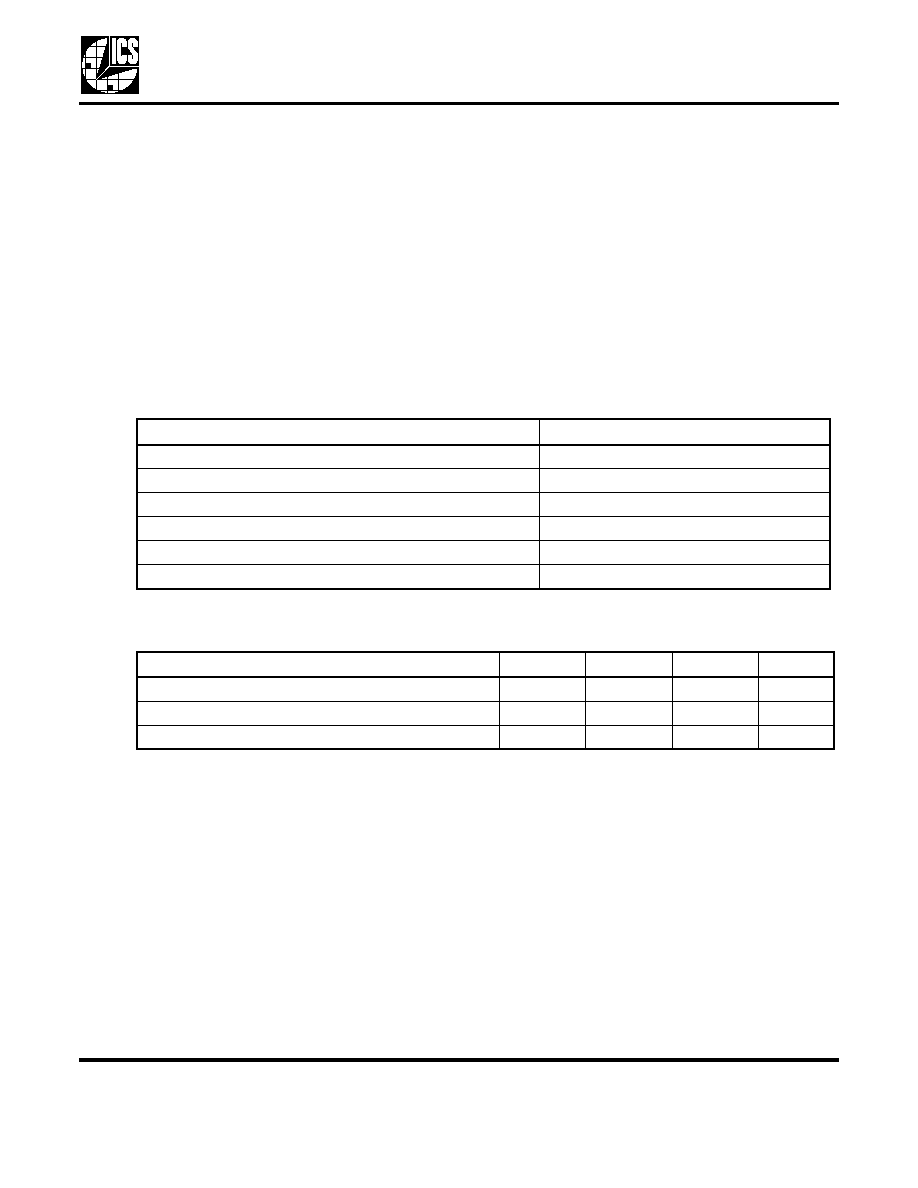
Recommended Operation Conditions
Item
Rating
Supply Voltage, VDD
7 V
All Inputs and Outputs
-0.5 V to VDD+0.5 V
Ambient Temperature under Bias
-55 to 125
∞C
Storage Temperature
-65 to +150
∞C
Junction Temperature
125
∞C
Power Dissipation
0.5 W
Parameter
Min.
Typ.
Max.
Units
Ambient Operating Temperature
0
+70
∞C
Power Supply Voltage (measured in respect to GND)
+4.5
+5.0
+5.5
V
Power Supply Voltage (measured in respect to GND)
+3.15
+3.3
+3.45
V
Multiplier and Zero Delay Buffer
MDS 2402 D
4
Revision 122104
Integrated Circuit Systems, Inc.
525 Race Street, San Jose, CA 95126
tel (408) 297-1201
www.icst.com
ICS2402
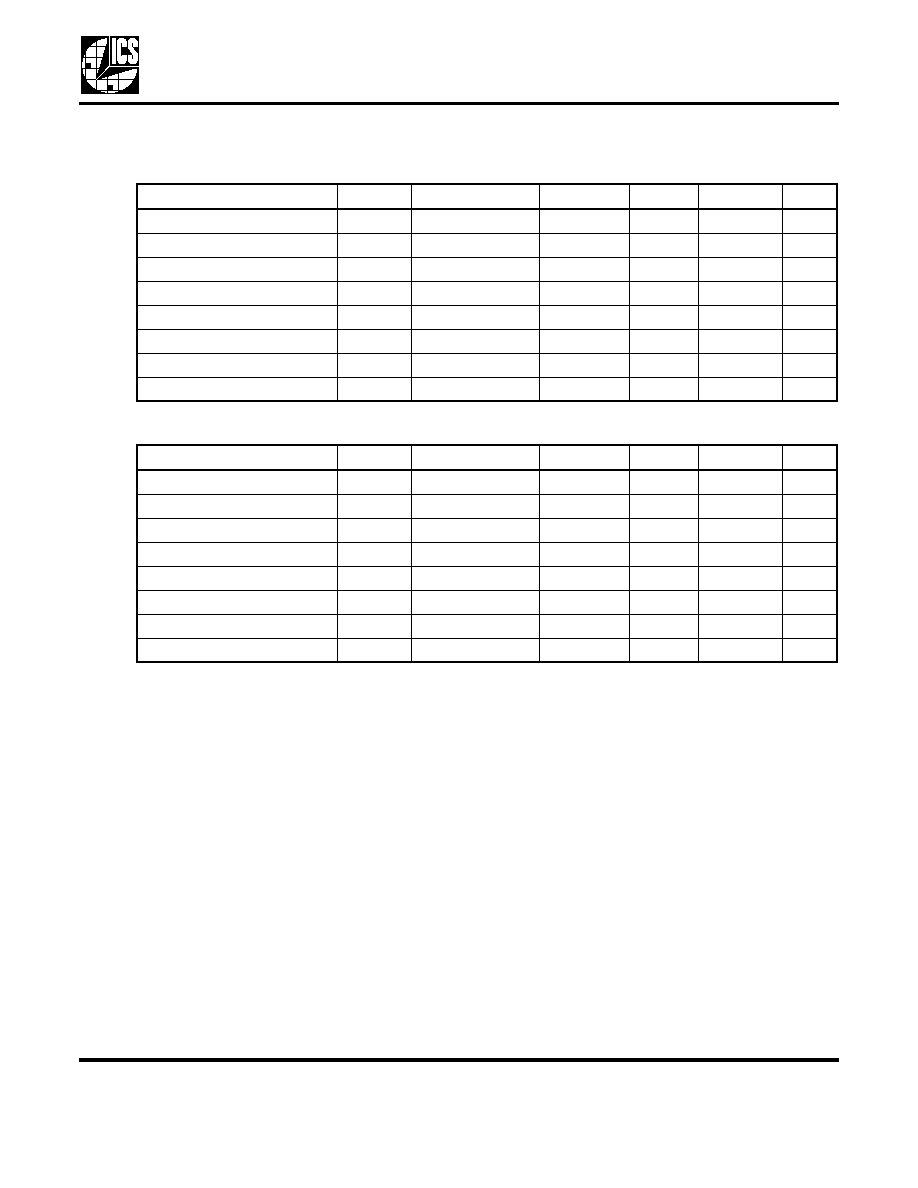
DC Electrical Characteristics
VDD = 3.3 V ±5%, Ambient Temperature 0 to +70
∞C
VDD = 5 V ±10%, Ambient Temperature 0 to +70
∞C
Parameter
Symbol Conditions
Min.
Typ.
Max.
Units
Operating Voltage
VDD
3.15
3.45
V
Operating Current
IDD
20
mA
Input High Voltage
V
IH
ICLK, FBIN, S0
2
V
Input Low Voltage
V
IL
ICLK, FBIN, S0
0.8
V
Output High Voltage
V
OH
I
OH
= -12 mA
2.4
V
Output Low Voltage
V
OL
I
OL
= 12 mA
0.4
V
Short Circuit Current
I
OS
CLK
±50
mA
Input Capacitance
C
IN
S0
5
pF
Parameter
Symbol Conditions
Min.
Typ.
Max.
Units
Operating Voltage
VDD
5 V
4.5
5.5
V
Operating Current
IDD
30
mA
Input High Voltage
V
IH
ICLK, FBIN, S0
0.7xVDD
V
Input Low Voltage
V
IL
ICLK, FBIN, S0
0.2xVDD
V
Output High Voltage
V
OH
I
OH
= -12 mA
4.5
V
Output Low Voltage
V
OL
I
OL
= 12 mA
0.5
V
Short Circuit Current
I
SC
Each output
±80
mA
Input Capacitance
C
IN
S0
5
pF
Multiplier and Zero Delay Buffer
MDS 2402 D
5
Revision 122104
Integrated Circuit Systems, Inc.
525 Race Street, San Jose, CA 95126
tel (408) 297-1201
www.icst.com
ICS2402
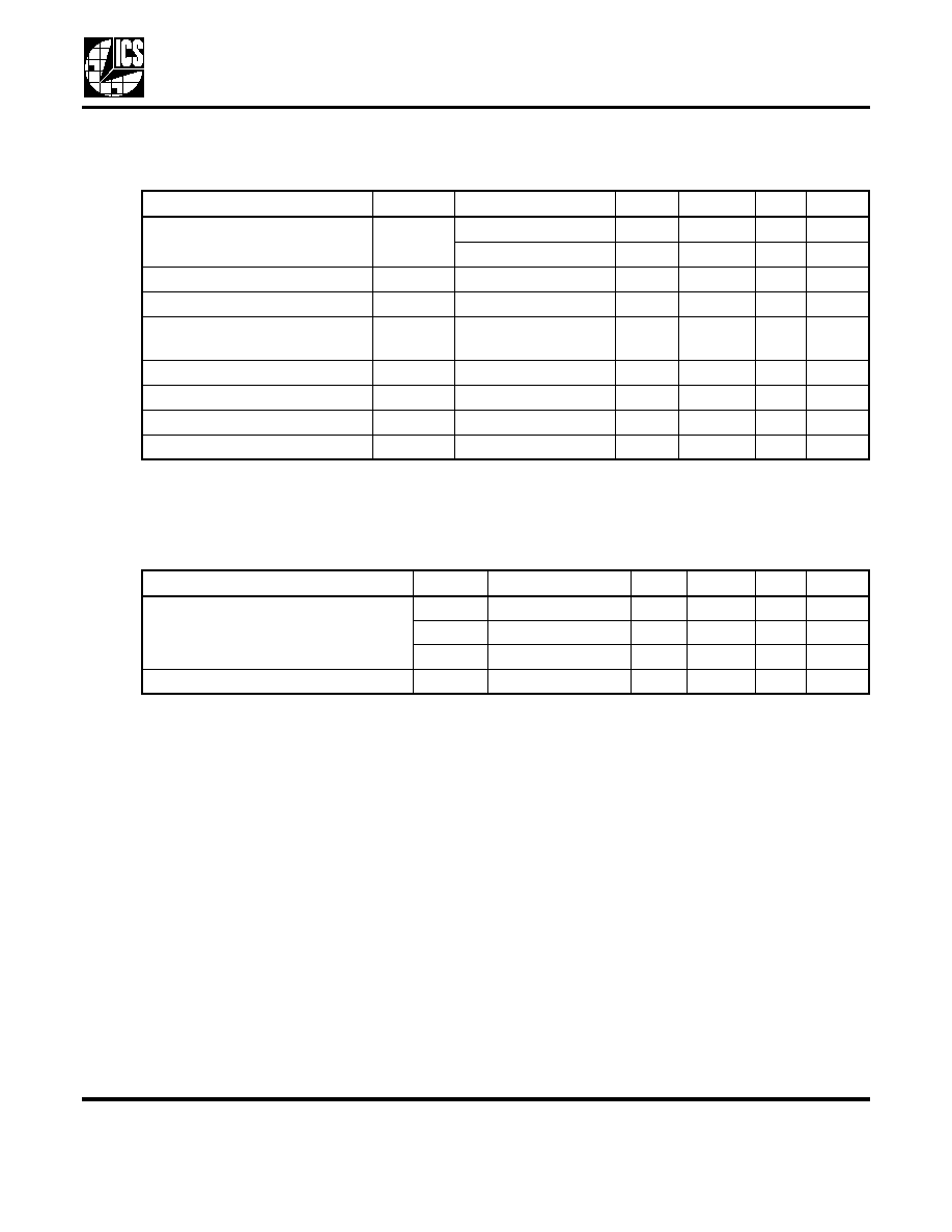
AC Electrical Characteristics
VDD = 3.3 V ±5%, or 5 V ±10%, Ambient Temperature 0 to +70
∞ C
Note 1: Assumes clocks with same rise time, measured from rising edges at VDD/2
Note 2: Measured with a 15 pF load.
Thermal Characteristics
Parameter
Symbol
Conditions
Min.
Typ.
Max.
Units
Input Frequency, ICLK
S0=1
10
80
MHz
S0=0
10
40
MHz
Output Frequency, CLK
10
80
MHz
Input to Output Jitter
CLK>20 MHz, Note 2
200
ps
Absolute Short-term Jitter,
peak-to-peak
Note 2
±100
ps
Input to Output Skew
Note 1
-600
600
ps
Output Clock Rise Time
20% to 80%, Note 2
1.5
ns
Output Clock Fall Time
80% to 20%, Note 2
1.5
ns
Output Clock Duty Cycle
At VDD/2, Note 2
45
50
55
%
Parameter
Symbol
Conditions
Min.
Typ.
Max.
Units
Thermal Resistance Junction to
Ambient
JA
Still air
150
∞C/W
JA
1 m/s air flow
140
∞C/W
JA
3 m/s air flow
120
∞C/W
Thermal Resistance Junction to Case
JC
40
∞C/W
Multiplier and Zero Delay Buffer
MDS 2402 D
6
Revision 122104
Integrated Circuit Systems, Inc.
525 Race Street, San Jose, CA 95126
tel (408) 297-1201
www.icst.com
ICS2402
Package Outline and Package Dimensions
(8-pin SOIC, 150 Mil. Body)
Package dimensions are kept current with JEDEC Publication No. 95
Ordering Information
"LF" denotes Pb (lead) free package.
While the information presented herein has been checked for both accuracy and reliability, Integrated Circuit
Systems (ICS) assumes no responsibility for either its use or for the infringement of any patents or other rights of
third parties, which would result from its use. No other circuits, patents, or licenses are implied. This product is
intended for use in normal commercial applications. Any other applications such as those requiring extended
temperature range, high reliability, or other extraordinary environmental requirements are not recommended
without additional processing by ICS. ICS reserves the right to change any circuitry or specifications without notice.
ICS does not authorize or warrant any ICS product for use in life support devices or critical medical instruments.
Part / Order Number
Marking
Shipping Packaging
Package
Temperature
ICS2402M
ICS2402M
Tubes
8-pin SOIC
0 to +70
∞ C
ICS2402MT
ICS2402M
Tape and Reel
8-pin SOIC
0 to +70
∞ C
ICS2402MLF
2402MLF
Tubes
8-pin SOIC
0 to +70
∞ C
ICS2402MLFT
2402MLF
Tape and Reel
8-pin SOIC
0 to +70
∞ C
INDEX
AREA
1 2
8
D
E
SEATING
PLANE
A1
A
e
- C -
B
.10 (.004)
C
C
L
H
h x 45
Millimeters
Inches
Symbol
Min
Max
Min
Max
A
1.35
1.75
.0532
.0688
A1
0.10
0.25
.0040
.0098
B
0.33
0.51
.013
.020
C
0.19
0.25
.0075
.0098
D
4.80
5.00
.1890
.1968
E
3.80
4.00
.1497
.1574
e
1.27 BASIC
0.050 BASIC
H
5.80
6.20
.2284
.2440
h
0.25
0.50
.010
.020
L
0.40
1.27
.016
.050
0
∞
8
∞
0
∞
8
∞
Multiplier and Zero Delay Buffer
MDS 2402 D
7
Revision 122104
Integrated Circuit Systems, Inc.
525 Race Street, San Jose, CA 95126
tel (408) 297-1201
www.icst.com
ICS2402
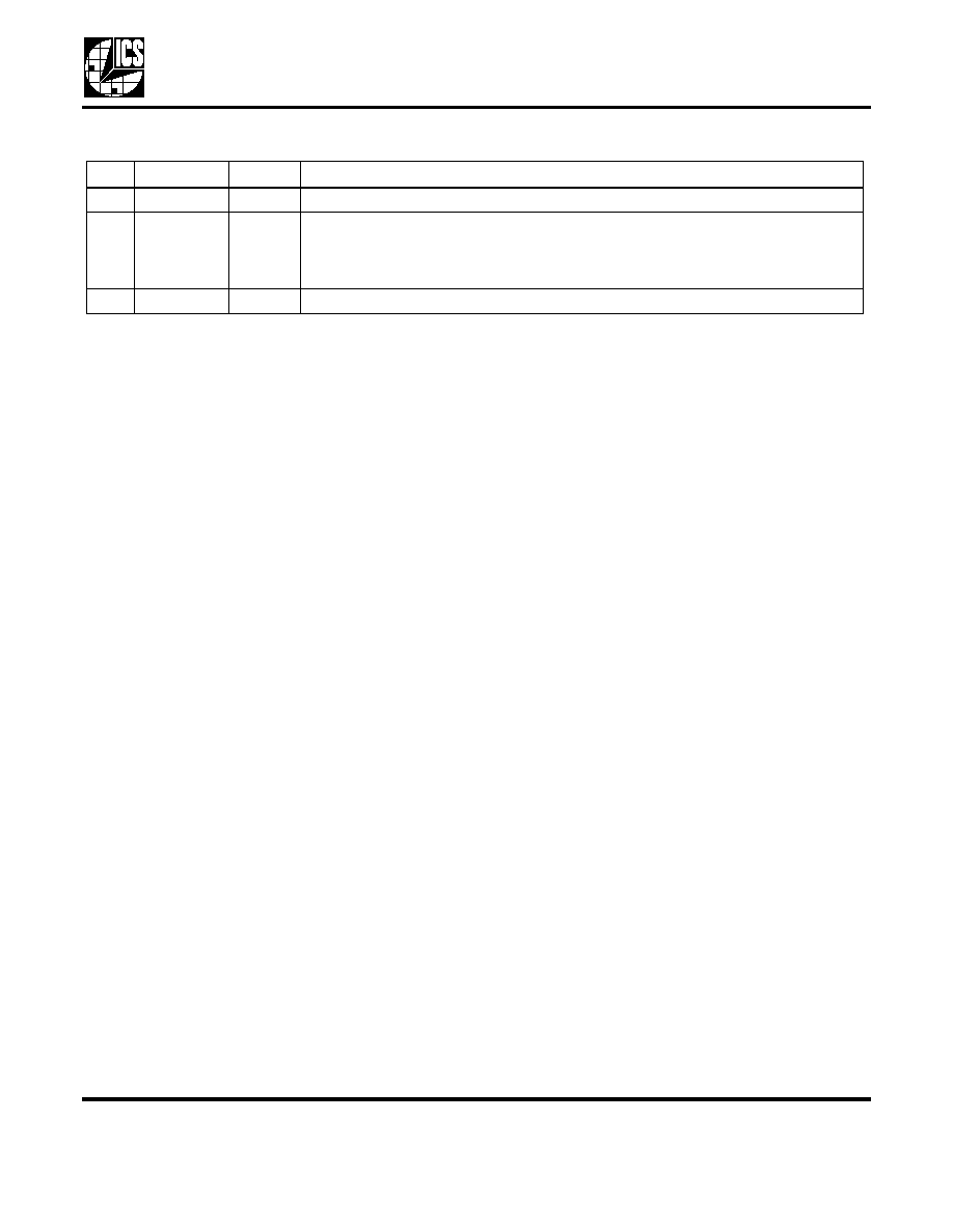
Revision History
Rev.
Originator
Date
Description of Change
B
P.Griffith
10/05/04
New device/datasheet for HP.
C
S. Gardner
11/04/04
Changed values for Abs. Jitter, Prop. Delay, and Output Clock Freq. in "Features" section;
removed secondary Input High/Low and Output High (CMOS) voltage specs in DC chars;
multiple updates to AC chars and added 5 V +/-10% rating; move from Preliminary to
Release.
D
P.Griffith
12/21/04
Added LF packaging and ordering information. Released from custom to standard device.