 | –≠–ª–µ–∫—Ç—Ä–æ–Ω–Ω—ã–π –∫–æ–º–ø–æ–Ω–µ–Ω—Ç: ICS2509 | –°–∫–∞—á–∞—Ç—å:  PDF PDF  ZIP ZIP |

Integrated
Circuit
Systems, Inc.
General Description
Features
ICS2509C
Block Diagram
3.3V Phase-Lock Loop Clock Driver
2509 C Rev C 06/15/01
Pin Configuration
24 Pin TSSOP
4.40 mm. Body, 0.65 mm. pitch
The ICS2509C is a high performance, low skew, low jitter
clock driver. It uses a phase lock loop (PLL) technology to
align, in both phase and frequency, the CLKIN signal with
the CLKOUT signal. It is specifically designed for use with
synchronous SDRAMs. The ICS2509C operates at 3.3V VCC
and drives up to nine clock loads.
One bank of five outputs and one bank of four outputs provide
nine low-skew, low-jitter copies of CLKIN. Output signal
duty cycles are adjusted to 50 percent, independent of the
duty cycle at CLKIN. Each bank of outputs can be enabled or
disabled separately via control (OEA and OEB) inputs. When
the OE inputs are high, the outputs align in phase and
frequency with CLKIN; when the OE inputs are low, the
outputs are disabled to the logic low state.
The ICS2509C does not require external RC filter
components. The loop filter for the PLL is included on-chip,
minimizing component count, board space, and cost. The
buffer mode shuts off the PLL and connects the input directly
to the output buffer. This buffer mode, the ICS2509C can be
use as low skew fanout clock buffer device. The ICS2509C
comes in 24 pin 173mil Thin Shrink Small-Outline package
(TSSOP) package.
∑
Meets or exceeds PC133 registered DIMM
specification 1.1
∑
Spread Spectrum Clock Compatible
∑
Distributes one clock input to one bank of five and one
bank of four outputs
∑
Separate output enable(OEA,OEB) for each output bank
∑
Operating frequency 25 MHz to 175 Mhz
∑
External feedback input (FBIN) terminal is used to
synchrionize the outputs to the clock input
∑
No external RC network required
∑
Operates at 3.3V Vcc
∑
Plastic 24-pin 173mil TSSOP package
FBIN
CLKIN
AVCC
OEA
OEB
PLL
CLKA0
FBOUT
CLKA1
CLKA2
CLKA3
CLKA4
CLKB0
CLKB1
CLKB2
CLKB3
AGND
VCC
CLKA0
CLKA1
CLKA2
GND
GND
CLKA3
CLKA4
VCC
OEA
FBOUT
CLKIN
VCC
CLKB0
CLKB1
GND
GND
CLKB2
CLKB3
VCC
OEB
FBIN
AVCC
ICS2509C
1
2
3
4
5
6
7
8
9
10
11
12
24
23
22
21
20
19
18
17
16
15
14
13
ICS reserves the right to make changes in the device data identified in
this publication without further notice. ICS advises its customers to
obtain the latest version of all device data to verify that any
information being relied upon by the customer is current and accurate.

2
ICS2509C
Pin Descriptions
Note:
1.
Weak pull-ups on these inputs
PIN NUM BER
PIN NAM E
TYPE
DESCR IPTION
1
AGND
PWR
Analog Ground
2, 10, 15
VCC
PWR
Power Supply (3.3V)
3
CLKA0
OUT
Buffered clock output, Bank A
4
CLKA1
OUT
Buffered clock output, Bank A
5
CLKA2
OUT
Buffered clock output, Bank A
6, 7, 18, 19
GND
PWR
Ground
8
CLKA3
OUT
Buffered clock output, Bank A
9
CLKA4
OUT
Buffered clock output, Bank A
11
OEA
1
IN
Output enable (has internal pull_up). When high, normal operation.
When low bank A clock outputs are disabled to a logic low state.
12
FBOUT
OUT
Feedback output
13
FBIN
IN
Feedback input
14
OEB
1
IN
Output enable (has internal pull_up). When high, normal operation.
When low bank B clock outputs are disabled to a logic low state.
16
CLKB3
OUT
Buffered clock output. Bank B
17
CLKB2
OUT
Buffered clock output. Bank B
20
CLKB1
OUT
Buffered clock output. Bank B
21
CLKB0
OUT
Buffered clock output. Bank B
22
VCC
PWR
Power Supply (3.3V) digital supply.
23
AVC C
IN
Analog power supp ly (3.3V). When input is ground PLL is off and
bypassed.
24
CLKIN
IN
Clock input
Functionality
OEA
OEB
AVCC
CLKA
(0:4 )
CLKB
(0:3)
FBOUT
Source
0
0
3.33
0
0
Driven
PLL
N
0
1
3.33
0
Driven
Driven
PLL
N
1
0
3.33
Driven
0
Driven
PLL
N
1
1
3.33
Driven
Driven
Driven
PLL
N
0
0
0
0
0
Driven
CLKIN
Y
0
1
0
0
Driven
Driven
CLKIN
Y
1
0
0
Driven
0
Driven
CLKIN
Y
1
1
0
Driven
Driven
Driven
CLKIN
Y
Test mode:
When AVC C is 0, shuts off the PLL and connects the input directly to the output buffers
Buffer M ode
INPUTS
OUTPUTS
PLL
Shutdown
3
ICS2509C
Absolute Maximum Ratings
Supply Voltage (AVCC) . . . . . . . . . . . . . . . . . . . AVCC < (V
cc
+ 0.7V)
Supply Voltage (VCC) . . . . . . . . . . . . . . . . . . . . 4.3 V
Logic Inputs . . . . . . . . . . . . . . . . . . . . . . . . . . . . GND ≠0.5 V to V
cc
+0.5 V
Ambient Operating Temperature . . . . . . . . . . . . 0∞C to +70∞C
Storage Temperature . . . . . . . . . . . . . . . . . . . . . . ≠65∞C to +150∞C
Stresses above those listed under Absolute Maximum Ratings may cause permanent damage to the device. These ratings are
stress specifications only and functional operation of the device at these or any other conditions above those listed in the
operational sections of the specifications is not implied. Exposure to absolute maximum rating conditions for extended
periods may affect product reliability.
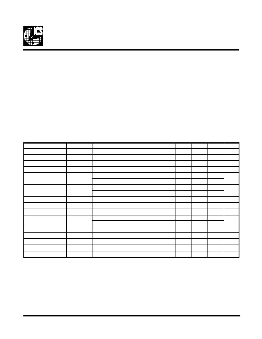
Electrical Characteristics - OUTPUT
T
A
= 0 - 70C; V
DD
= V
DDL
= 3.3 V +/-10%; C
L
= 20 - 30 pF; R
L
= 470 Ohms (unless otherwise stated)
PARAMETER
SYMBOL
CONDITIONS
MIN
TYP
MAX
UNITS
Output Impedance
R
DSP
V
O
= V
DD
*(0.5)
36
Output Impedance
R
DSN
V
O
= V
DD
*(0.5)
32
Output High Voltage
V
OH
I
OH
= -8 mA
2.4
2.9
V
Output Low Voltage
V
OL
I
OL
= 8 mA
0.25
0.4
V
V
OH
= 2.4 V
-26
-13.6
V
OH
= 2.0 V
-37
-22
V
OL
= 0.8 V
19
25
V
OL
= 0.55 V
13
17
Rise Time
1
T
r
V
OL
= 0.8 V, V
OH
= 2.0 V
0.5
1.4
2.1
ns
Fall Time
1
T
f
V
OH
= 2.0 V, V
OL
= 0.8 V
0.5
1.5
2.7
ns
Duty Cycle
1
D
t
V
T
= 1.5 V;C
L
=30 pF
45
50
55
%
at 66-100 MHz ; loaded outputs
52
100
at 133 MHz ; loaded outputs
39
75
Absolute Jitter
1
Tjabs
10000 cycles; C
L
= 30 pF
57
ps
Skew
1
T
sk
V
T
= 1.5 V (Window) Output to Output
80
150
ps
Phase error
1
T
pe
V
T
= Vdd/2; CLKIN-FBIN
-150
40
150
ps
Phase error Jitter
1
T
pe
3
V
T
= Vdd/2; CLKIN-FBIN; Delay Jitter
-50
35
50
ps
Delay Input-Output
1
D
R1
V
T
= 1.5 V; PLL_EN = 0
3.3
3.7
ns
1
Guaranteed by design, not 100% tested in production.
Cycle to Cycle jitter
1
Tcyc-cyc
ps
Output High Current
Output Low Current
I
OH
I
OL
mA
mA
4
ICS2509C
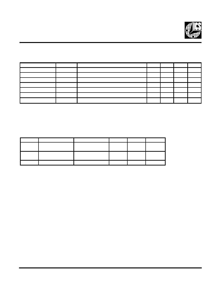
Symbol
Parameter
Test Conditions
Min.
Max.
Unit
Fclk
Input clock frequency
25
175
MHz
Input clock frequency
duty cycle
40
60
%
Stabilization time
After power up
1
ms
Timing requirements over recommended ranges of supply
voltage and operating free-air temperature
Note: Time required for the PLL circuit to obtain phase lock of its feedback signal to its reference
In order for phase lock to be obtained, a fixed-frequency, fixed-phase reference signal must be
Until phase lock is obtained, the specifications for parameters given in the switching characteristics table are not
Electrical Characteristics - Input & Supply
T
A
= 0 - 70C; Supply Voltage V
DD
= 3.3 V +/-10% (unless otherwise stated)
PARAMETER
SYMBOL
CONDITIONS
MIN
TYP
MAX
UNITS
Input High Voltage
V
IH
2
V
DD
+0.3
V
Input Low Voltage
V
IL
V
SS
-0.3
0.8
V
Input High Current
I
IH
V
IN
= V
DD
0.1
100
uA
Input Low Current
I
IL
V
IN
= 0 V;
19
50
uA
Operating current
I
DD1
C
L
= 0 pF; F
IN
@ 66M
140
170
mA
Input Capacitance
C
IN
1
Logic Inputs
4
pF
Output Capacitance
C
O
1
Logic Outputs
8
pF
1
Guarenteed by design, not 100% tested in production.
5
ICS2509C
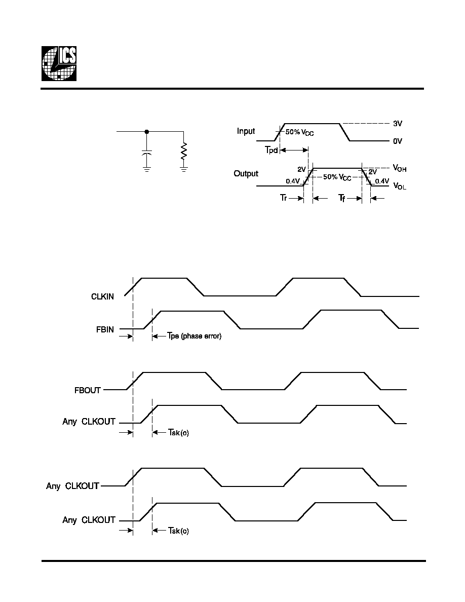
PARAMETER MEASUREMENT INFORMATION
Figure 1. Load Circuit for Outputs
Notes:
1.
C
L
includes probe and jig capacitance.
2.
All input pulses are supplied by generators having the following
characteristics:
PRR
133 MHz, Z
O
= 5 0
,
T
r
1.2 ns, T
f
1.2 ns.
3.
The outputs are measured one at a time with one transition per measurement.
30 pF
500
From Output
Under Test
Figure 2. Voltage Waveforms
Propagation Delay Times
Figure 3. Phase Error and Skew Calculations
6
ICS2509C
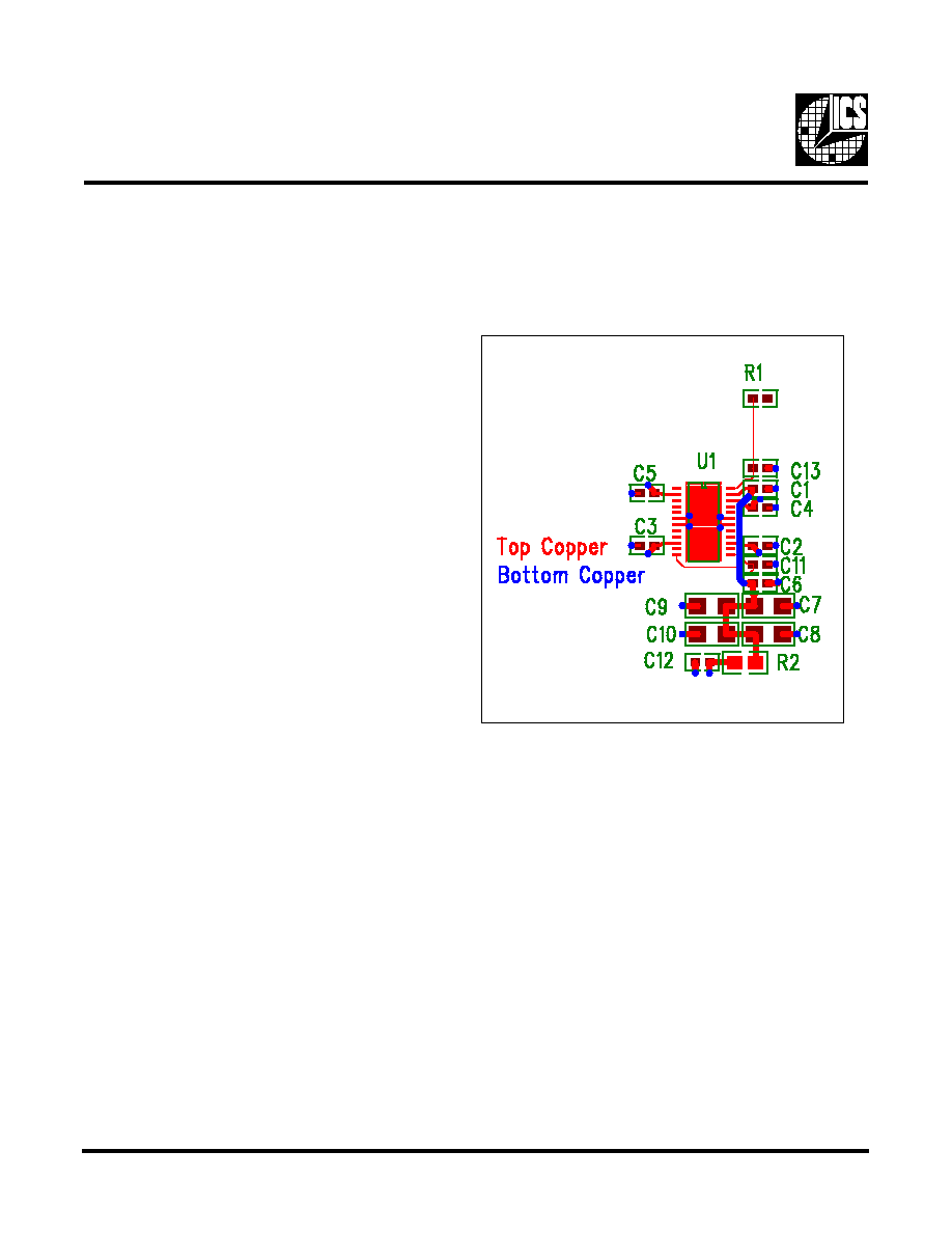
General Layout Precautions:
An ICS2509C is used as an example. It is similar to the
ICS2510C. The same rules and methods apply.
1)
Use copper flooded ground on the top signal layer
under the clock buffer The area under U1 in figure 1
on the right is an example.
2)
Use power vias for power and ground. Vias 20 mil or
larger in diameter have lower high frequency
impedance. Vias for signals may be minimum drill
size.
3)
Make all power and ground traces are as wide as the
via pad for lower inductance.
4)
VAA for pin 23 has a low pass RC filter to decouple
the digital and analog supplies. C9-11 may be replaced
with a single low ESR (0.8 ohm or less) device with
the same total capacitance.
5)
Notice that ground vias are never shared.
6)
All VCC pins have a decoupling capacitor. Power is
always routed from the plane connection via to the
capacitor pad to the VCC pin on the clock buffer.
7)
Component R1 is located at the clock source.
Component Values:
C1= As necessary for delay adjust
C[7:2]=.01uF
C8,C13=0.1uF
C[11:9]=4.7Uf
R1=10 ohm. Locate at driver
R2=10 ohm.
Figure 1.

7
ICS2509C
Ordering Information
ICS2509CyG-T
Designation for tape and reel packaging
Pattern Number (2 or 3 digit number for parts with ROM code patterns)
Package Type
G=TSSOP
Revision Designator (will not correlate with datasheet revision)
Device Type (consists of 3 or 4 digit numbers)
Prefix
ICS, AV = Standard Device
Example:
ICS XXXX y G - PPP - T
ICS reserves the right to make changes in the device data identified in
this publication without further notice. ICS advises its customers to
obtain the latest version of all device data to verify that any
information being relied upon by the customer is current and accurate.
4.40 mm. Body, 0.65 mm. pitch TSSOP
(173 mil)
(0.0256 Inch)
INDEX
AREA
INDEX
AREA
1 2
1 2
N
D
E1
E
SEATING
PLANE
SEATING
PLANE
A1
A
A2
e
- C -
- C -
b
c
L
aaa
C
MIN
MAX
MIN
MAX
A
--
1.20
--
.047
A1
0.05
0.15
.002
.006
A2
0.80
1.05
.032
.041
b
0.19
0.30
.007
.012
c
0.09
0.20
.0035
.008
D
E
E1
4.30
4.50
.169
.177
e
L
0.45
0.75
.018
.030
N
0∞
8∞
0∞
8∞
aaa
--
0.10
--
.004
VARIATIONS
MIN
MAX
MIN
MAX
24
7.70
7.90
.303
.311
10-0035
SYMBOL
In Millimeters
In Inches
COMMON DIMENSIONS
COMMON DIMENSIONS
SEE VARIATIONS
SEE VARIATIONS
6.40 BASIC
0.252 BASIC
0.65 BASIC
0.0256 BASIC
SEE VARIATIONS
SEE VARIATIONS
N
D mm.
D (inch)
Reference Doc.: JEDEC Publication 95, MO-153