
ICS307
Serially Programmable Clock Source
MDS 307 D
1
Revision 042501
Integrated Circuit Systems, Inc. ∑ 525 Race Street ∑ San Jose ∑CA∑95126∑(408) 295-9800tel ∑www.icst.com
∑ Packaged as 16 pin narrow SOIC
∑ Highly accurate frequency generation
∑ Serially programmable: user determines
the output frequency via a 3 wire interface.
∑ Eliminates need for custom quartz
∑ Input crystal frequency of 5 - 27 MHz
∑ Output clock frequencies up to 200 MHz
∑ Power Down Tri-State mode
∑ Very low jitter
∑ Operating voltages of 3.0 to 5.5 V
∑ 25 mA drive capability at TTL levels
∑ Industrial temperature available
The ICS307-01 and ICS307-02 are versatile
serially programmable clock sources which take
up very little board space.
They can generate any frequency from 6 to
200 MHz, and have a second configurable
output. The outputs can be reprogrammed on
the fly, and will lock to a new frequency in 10 ms
or less. Smooth transitions (in which the clock
duty cycle remains roughly 50%) are guaranteed
if the output divider is not changed.
The devices include a PDTS pin which tri-states
the output clocks and powers down the entire
chip.
The ICS307-02 features a default clock output
at start-up and is recommended for all new
designs.
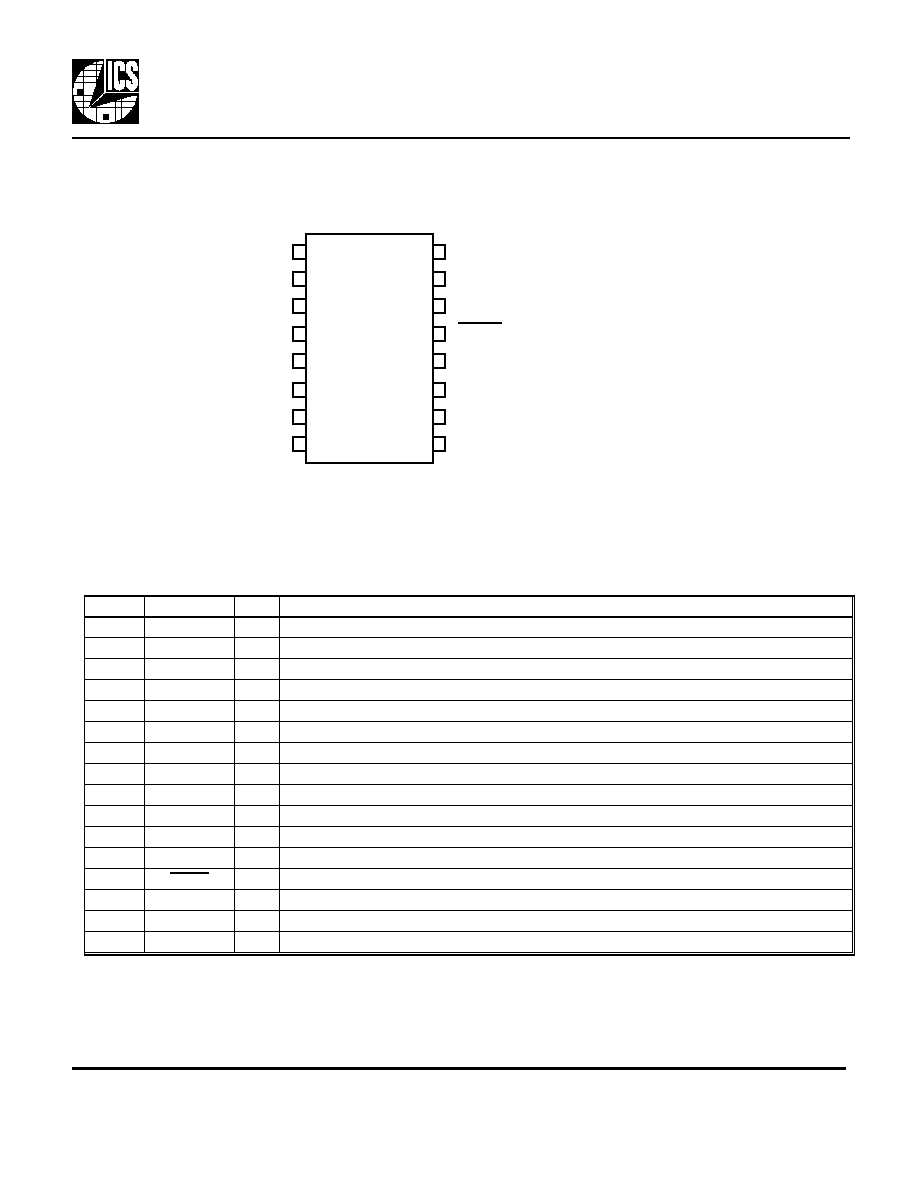
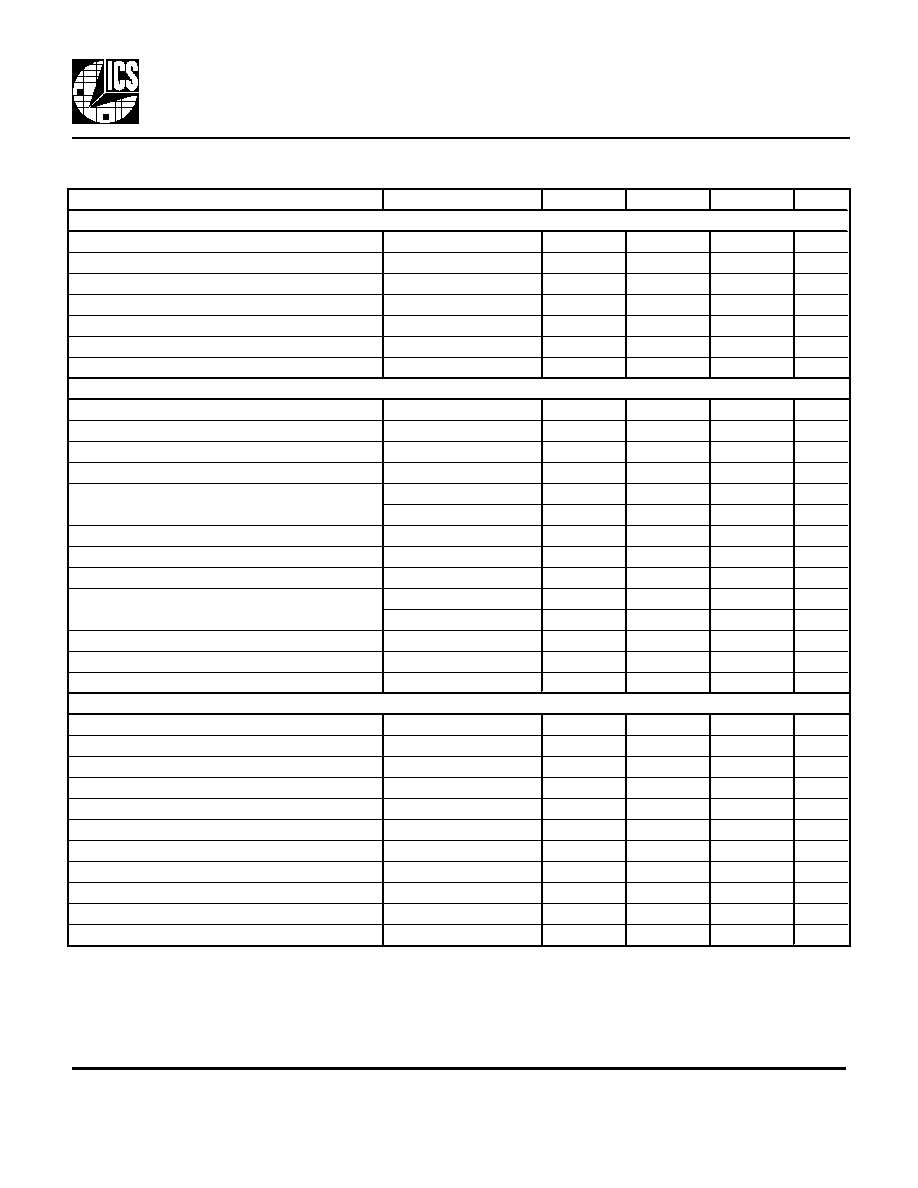
Block Diagram
Description
Features
Crystal or
clock input
X1/ICLK
X2
Reference
Divider
Phase Comparator,
Charge Pump,
and Loop Filter
Crystal
Oscillator
VCO
Divider
VCO
Output
Buffer
VDD GND
CLK1
Output
Buffer
CLK2
R6:R0
V8:V0
S2:S0
3
9
7
Output
Divider
Function
Select
F1:F0
2
2
3
2
C1:C0
S2:S0
F1:F0
TTL
TTL
C1:C0
SCLK
Shift
Register
DATA
STROBE
PDTS
ICS307
Serially Programmable Clock Source
MDS 307 D
2
Revision 042501
Integrated Circuit Systems, Inc. ∑ 525 Race Street ∑ San Jose ∑CA∑95126∑(408) 295-9800tel ∑www.icst.com
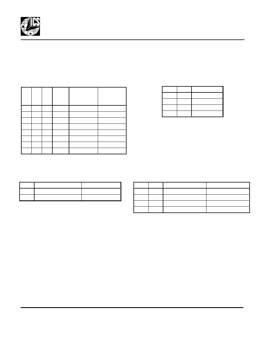
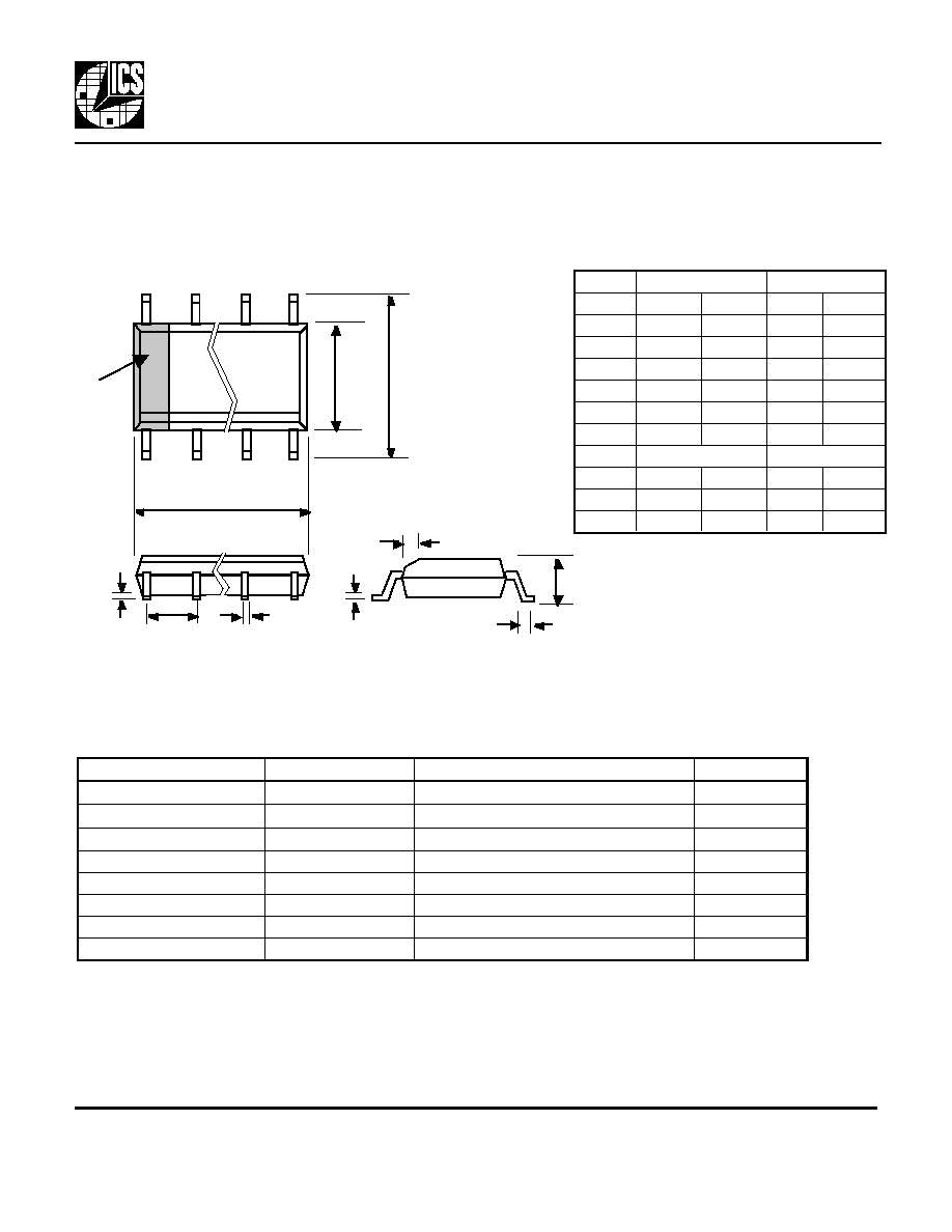
Pin Assignment
Pin Description
Type: XI, XO=crystal connections, I = Input, O = output, P = power supply connection
Number
Name
Type Description
1
X1/ICLK
XI
Crystal connection (REF frequency). Connect to a parallel resonant crystal, or an input clock .
2
NC
-
No Connect.
3
VDD
P
Connect to +3.3V or +5V.
4
NC
-
No Connect.
5
GND
P
Connect to ground.
6
CLK2
O
Output clock 2, determined by F0-F1. Can be reference, ref/2, CLK1/2 or off.
7
NC
-
No Connect.
8
SCLK
I
Serial clock. See timing diagram.
9
STROBE
I
Strobe to load data. See timing diagram.
10
NC
-
No Connect.
11
CLK1
O
Output clock 1, determined by R0-R6, V0-V8, S0-S2 and input frequency.
12
DATA
I
Data Input. Serial input for three words which set the output clock(s).
13
PDTS
I
Powers down entire chip, tri-states CLK1 and CLK2 outputs, when low. Internal pull-up.
14
NC
-
No Connect.
15
NC
-
No Connect.
16
X2
XO Input crystal connection. Connect to a crystal, or leave unconnected for clock input.
1
8
2
3
4
7
6
5
X1/ICLK
X2
VDD
16 pin Narrow
(0.150") SOIC
DATA
CLK2
CLK1
NC
NC
NC
NC
NC
NC
GND
SCLK
STROBE
PDTS
16
15
14
13
12
11
10
9
ICS307

ICS307
Serially Programmable Clock Source
MDS 307 D
3
Revision 042501
Integrated Circuit Systems, Inc. ∑ 525 Race Street ∑ San Jose ∑CA∑95126∑(408) 295-9800tel ∑www.icst.com
Determining the Output Frequency
On power-up the ICS307-01 on-chip registers can have random values, so almost any frequency may be
output from the part. CLK1 will always have some clock signal present, but CLK2 could possibly be OFF
(low).
The ICS307-02 on-chip registers are initially configured to provide a x1 output clock on both the CLK1
and CLK2 outputs. The output frequency will be the same as the input clock or crystal. This is useful if
the ICS307 will provide the initial system clock at power-up. Since this feature is an advantage in most
systems, the ICS307-02 is recommended for new designs.
With programming, the user has full control in changing the desired output frequency to any value over the
range shown in Table 1 on page 4. The output of the ICS307 can be determined by the following simple
equation:
To determine the best combination of VCO, reference, and output dividers, contact ICS application
engineering. You may also fax this page to ICS at 408 295 9818(fax). Be sure to indicate the following:
Your Name ________________ Company Name___________________ Telephone_________________
Respond by e-mail (list your e-mail address) __________________or fax number ___________________
Desired input crystal_______ or clock_______ (in MHz) Desired output frequency_______________
REF Output_______VDD = 3.3V or 5V _______ Duty Cycle: 40-60% _____ or 45-55% required____
CLK1 frequency = Input frequency ∑ 2 ∑
(VDW+8)
(RDW+2)(OD)
Also, the following operating ranges should be observed:
55 MHz < Input frequency ∑ 2 ∑
(VDW+8)
(RDW+2)
< 400 MHz
200 kHz <
Input Frequency
(RDW+2)
Where
VCO Divider Word (VDW) = 4 to 511 (0, 1, 2, 3 are not permitted)
Reference Divider Word (RDW) = 1 to 127 (0 is not permitted)
Output Divider = values on page 4
Commercial temperature range.
Industrial temperature limits are
60 MHz to 360 MHz.
ICS307
Serially Programmable Clock Source
MDS 307 D
4
Revision 042501
Integrated Circuit Systems, Inc. ∑ 525 Race Street ∑ San Jose ∑CA∑95126∑(408) 295-9800tel ∑www.icst.com
Setting the Device Characteristics
The tables below show the settings which can be configured, in addition to the VCO and Reference dividers.
CLK1
Maximum
Max. Freq.
S2
S1
S0
Output
Frequency
Industrial
Divide
5 V or 3.3 V
Version
0
0
0
10
40
36
0
0
1
2
200
180
0
1
0
8
50
45
0
1
1
4
100
90
1
0
0
5
80
72
1
0
1
7
55
50
1
1
0
3
135
120
1
1
1
6
67
60
Table 1. Output Divide and
Maximum Output Frequency
Table 2. CLK2 Output
TTL
Duty cycle measured at
Recommended VDD
0
1.4V
5 V
1
VDD/2
3.3 V
Table 3. Output Duty Cycle Configuration
C1
C0
VDD = 5 V
VDD = 3.3 V
0
0
22.3 - 0.083 f
22.1 - 0.094 f
0
1
23.1 - 0.093 f
22.9 - 0.108 f
1
0
23.7 - 0.106 f
23.5 - 0.120 f
1
1
24.4 - 0.120 f
24.2 - 0.135 f
Table 4. Crystal Load Capacitance
Note: f is the crystal frequency, between 10 and
27 MHz. Effective load capacitance will be higher
for crystal frequencies lower than 10 MHz. If a
clock input is used, set C1 = 0 and C0 = 0.
Note: The TTL bit optimizes the duty cycle at
different VDD. When VDD is 5 V, set to 0
for a near-50% duty cycle with TTL levels.
When VDD is 3.3 V, set this bit to a 1, so the
50% duty cycle is achieved at VDD/2.
F1
F0
CLK2
0
0
REF
0
1
REF/2
1
0
OFF (Low)
1
1
CLK1/2
0 = Connect directy to ground
1 = Connect directly to VDD
ICS307
Serially Programmable Clock Source
MDS 307 D
5
Revision 042501
Integrated Circuit Systems, Inc. ∑ 525 Race Street ∑ San Jose ∑CA∑95126∑(408) 295-9800tel ∑www.icst.com
MSB
LSB
R6:R0
Reference Divider Word (RDW)
V8:V0
VCO Divider Word (VDW)
S2:S0
Output Divider Select (OD)
F1:F0
Function of CLK2 Output
TTL
Duty Cycle Setting
C1:C0
Internal Load Capacitance for Crystal
MSB
LSB
MSB
LSB
C1 C0
TTL
F1 F0
S2
S1
S0
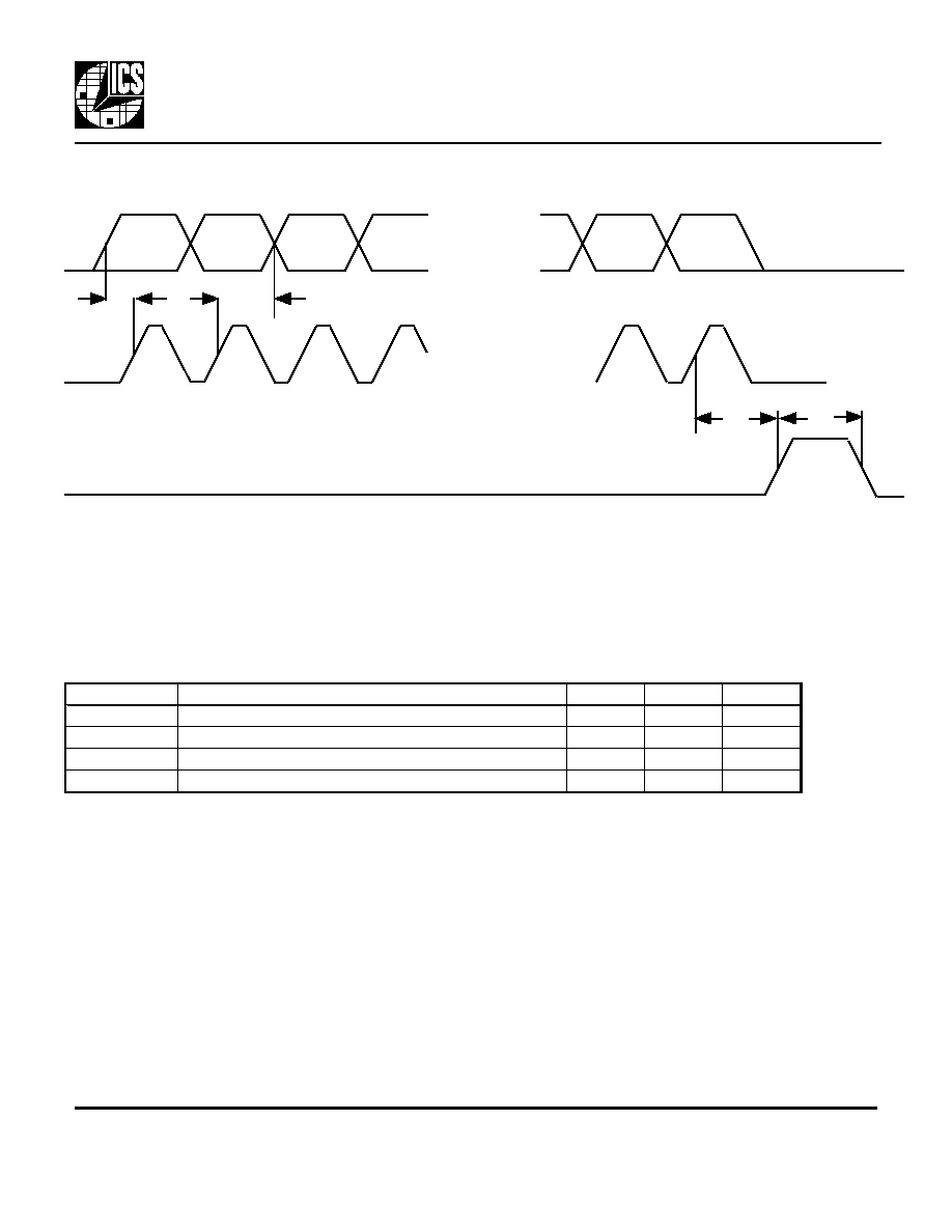
Configuring the ICS307
The ICS307 can be programmed to set the output functions and frequencies. The three data bytes are
written to the DATA pin, in this order:
V8 V7 V6 V5 V4 V3 V2 V1
V0 R6 R5 R4 R3 R2 R1 R0
C1 is loaded into the port first and R0 last.
Programming Example
To generate 66.66 MHz from a 14.31818 MHz input, the RDW should be 59, the VDW should be 276,
and the Output Divide is 2. Selecting the minimum internal load capacitance, CMOS duty cycle, and CLK2
to be OFF means that the following three bytes are sent to the ICS307:
00110001
10001010
00111011
Byte 1
Byte 2
Byte 3
As shown in Figure 2, after these 24 bits are clocked into the ICS307, taking STROBE high will send this data
to the internal latch, and the CLK output will lock within 10 ms.
NOTE: If STROBE is in the high state and SCLK is pulsed, DATA is clocked directly to the internal latch
and the output conditions will change accordingly. Although this will not damage the ICS307, it is
recommended that STROBE be kept low while DATA is being clocked into the ICS307 in order to avoid
unintended changes on the output clocks.
Power up default values for ICS 307-02
0
0
1
0
0
0
1
1
0
0
0
0
0
1
0
0
0
0
0
0
0
1
1
0
The input frequency will come from both outputs.
ICS307
Serially Programmable Clock Source
MDS 307 D
6
Revision 042501
Integrated Circuit Systems, Inc. ∑ 525 Race Street ∑ San Jose ∑CA∑95126∑(408) 295-9800tel ∑www.icst.com
External Components / Crystal Selection
The ICS307 require a 0.01µF decoupling capacitor to be connected between VDD and GND. It must be
connected close to the ICS307 to minimize lead inductance. A 33
terminating resistor can be used in
series with the CLK1 and CLK2 outputs. A parallel resonant, fundamental mode crystal with a load
(correlation) capacitance of C should be used, where C is the value calculated from Table 4. For crystals
with a specified load capacitance greater than C, additional crystal capacitors may be connected from each
of the pins X1 and X2 to Ground as shown in the Block Diagram on page 1. The value (in pF) of these
crystal caps should be = (CL-C)*2, where CL is the crystal load capacitance in pF. These external
capacitors are only required for applications where the exact frequency is critical. For a clock input,
connect to X1 and leave X2 unconnected (no capacitors on either pin).
Figure 2. Timing Diagram for Programming the ICS307
Parameter
Condition
Min
Max
Units
Setup time.
10
ns
Hold time after SCLK.
10
ns
Data wait time.
10
ns
Strobe pulse width
40
ns
AC Parameters for Writing to the ICS307
DATA
C1
C0
TTL
F1
R1
R0
∑ ∑ ∑
∑ ∑ ∑
SCLK
STROBE
tsetup
thold
tw
ts
t
SETUP
t
HOLD
t
w
t
s
Parameter
Conditions
Minimum
Typical
Maximum
Units
ABSOLUTE MAXIMUM RATINGS (Note 1)
Supply Voltage, VDD
Referenced to GND
7
V
Inputs
Referenced to GND
-0.5
VDD+0.5
V
Clock Output
Referenced to GND
-0.5
VDD+0.5
V
Ambient Operating Temperature
0
70
∞C
Ambient Operating Temperature, Industrial
I version
-40
85
∞C
Soldering Temperature
Max of 10 seconds
260
∞C
Storage temperature
-65
150
∞C
DC CHARACTERISTICS (VDD = 5.0 V unless otherwise noted)
DC CHARACTERISTICS (VDD = 5.0 V unless otherwise noted)
Operating Voltage, VDD
3
5.5
V
Input High Voltage, VIH, X1/ICLK only
ICLK (Pin 1)
(VDD/2)+1
VDD/2
V
Input Low Voltage, VIL, X1/ICLK only
ICLK (Pin 1)
VDD/2
(VDD/2)-1
V
Input High Voltage, VIH
2
V
Input Low Voltage, VIL
PDTS, ICS307-01 only
0.4
V
All other inputs,-01 & -02
0.8
Output High Voltage, VOH, CMOS level
IOH=-4 mA
VDD-0.4
V
Output High Voltage, VOH
IOH=-25 mA
2.4
V
Output Low Voltage, VOL
IOL=25 mA
0.4
V
IDD Operating Supply Current, 20 MHz crystal
No Load, 100 MHz out
26
mA
100MHz out,VDD=3.3V
13
mA
Short Circuit Current
CLK1 and CLK2 outputs
±70
mA
On-Chip Pull-up Resistor
Pin 13
270
k
Input Capacitance
4
pF
AC CHARACTERISTICS
Input Frequency, crystal input (must be fundamental)
5
27
MHz
Input Frequency, clock input
2
50
MHz
Output Frequency (See Table 1)
VDD = 3.0 to 5.5V
6
200
MHz
Output Frequency (see Table 1), I version
VDD = 3.0 to 5.5V
6
180
MHz
Output Clock Rise Time
0.8 to 2.0V
1
ns
Output Clock Fall Time
2.0 to 0.8V
1
ns
Output Clock Duty Cycle, even output divides
At duty cycle level
45
49 to 51
55
%
Output Clock Duty Cycle, odd output divides
At duty cycle level
40
60
%
Power-up time, STROBE goes high until CLK out
3
10
ms
Absolute Maximum Clock Period Jitter
Deviation from mean
±120
ps
One Sigma Clock Period Jitter
50
ps
ICS307
Serially Programmable Clock Source
MDS 307 D
7
Revision 042501
Integrated Circuit Systems, Inc. ∑ 525 Race Street ∑ San Jose ∑CA∑95126∑(408) 295-9800tel ∑www.icst.com
Electrical Specifications
Notes:
1. Stresses beyond those listed under Absolute Maximum Ratings could cause permanent damage to the device. Prolonged exposure
to levels above the operating limits but below the Absolute Maximums may affect device reliability.
2. Typical values are at 25∞C.
ICS307
Serially Programmable Clock Source
MDS 307 D
8
Revision 042501
Integrated Circuit Systems, Inc. ∑ 525 Race Street ∑ San Jose ∑CA∑95126∑(408) 295-9800tel ∑www.icst.com
While the information presented herein has been checked for both accuracy and reliability, Integrated Circuit Systems, Inc. (ICS) assumes no responsibility for either its use or for the
infringement of any patents or other rights of third parties, which would result from its use. No other circuits, patents, or licenses are implied. This product is intended for use in
normal commercial applications. Any other applications such as those requiring extended temperature range, high reliability, or other extraordinary environmental requirements are
not recommended without additional processing by ICS. ICS reserves the right to change any circuitry or specifications without notice. ICS does not authorize or warrant any ICS
product for use in life support devices or critical medical instruments.
Ordering Information
Part/Order Number
Marking
Package
Temperature
ICS307M-01
ICS307M-01
16 pin SOIC
0 to 70 ∞C
ICS307M-01T
ICS307M-01
16 pin SOIC on tape and reel
0 to 70 ∞C
ICS307M-01I
ICS307M-01I
16 pin SOIC
-40 to 85∞C
ICS307M-01IT
ICS307M-01I
16 pin SOIC on tape and reel
-40 to 85∞C
ICS307M-02
ICS307M-02
16 pin SOIC
0 to 70 ∞C
ICS307M-02T
ICS307M-02
16 pin SOIC on tape and reel
0 to 70 ∞C
ICS307M-02I
ICS307M-02I
16 pin SOIC
-40 to 85∞C
ICS307M-02IT
ICS307M-02I
16 pin SOIC on tape and reel
-40 to 85∞C
16 pin SOIC narrow
Inches
Inches
Millimeters
Millimeters
Symbol
Min
Max
Min
Max
A
0.0532
0.0688
1.35
1.75
A1
0.0040
0.0098
0.10
0.24
B
0.0130
0.0200
0.33
0.51
C
0.0075
0.0098
0.19
0.24
D
0.3859
0.3937
9.80
10.00
E
0.1497
0.1574
3.80
4.00
e
.050 BSC
.050 BSC
1.27 BSC
1.27 BSC
H
0.2284
0.2440
5.80
6.20
h
0.0099
0.0195
0.25
0.50
L
0.0160
0.0500
0.41
1.27
B
D
E
H
e
A1
C
A
h x 45∞
L
INDEX
AREA
1
2
Package Outline and Package Dimensions
(
For current dimensional specifications, see JEDEC Publication No. 95.)