 | –≠–ª–µ–∫—Ç—Ä–æ–Ω–Ω—ã–π –∫–æ–º–ø–æ–Ω–µ–Ω—Ç: ICS408M | –°–∫–∞—á–∞—Ç—å:  PDF PDF  ZIP ZIP |

ICS408
MDS 408 B
1
Revision 032602
Integrated Circuit Systems, Inc.
q
525 Race Street, San Jose, CA 95126
q
tel (408) 295-9800
q
www.icst.com
PC P
ERIPHERAL
C
LOCK
Description
The ICS408 is a cost-effective clock synthesizer
developed to minimize component count for PC
peripheral applications. The device supports a
common, low cost 14.31818 MHz crystal using an
on-chip crystal oscillator. The device locks all output
frequencies to enhance system performance. By
supporting common PC peripheral interface
frequencies of 25MHz, 24.576 MHz, and 40/80 MHz,
the ICS408 lowers chip count, reducing system cost
and improving reliability.
The ICS408 utilizes a low pin count 8-pin SOIC
package to optimize board space.
ICS is a leader in low jitter and low power consumer
application clock sources. These devices are capable
of supporting CCD, video, audio, USB, CPU, and other
peripherals.
Features
∑
Low operating voltage of 3.3V
∑
On-chip oscillator supports 14.31818 MHz crystal
∑
Fixed 24.576 MHz clock
∑
Fixed 25MHz clock
∑
40/80 MHz selected on rising edge of OE/LAT pin
∑
Power consumption of 15 mA (typ) extends battery
life
∑
Duty cycle of 45 to 55%
∑
Packaged in 8 pin SOIC
∑
Contact ICS for custom frequency requirements
Block Diagram
2 4 .5 7 6 M
C ry s ta l
O s c illa to r
X 1
X 2
1 4 .3 1 8 1 8 M H z
fu n d a m e n ta l
c ry s ta l
P L L /C lo c k
S y n th e s is
C irc u itry
2 5 M
4 0 /8 0 M
V D D
G N D
O E /L A T
PC P
ERIPHERAL
C
LOCK
MDS 408 B
2
Revision 032602
Integrated Circuit Systems, Inc.
q
525 Race Street, San Jose, CA 95126
q
tel (408) 295-9800
q
www.icst.com
ICS408
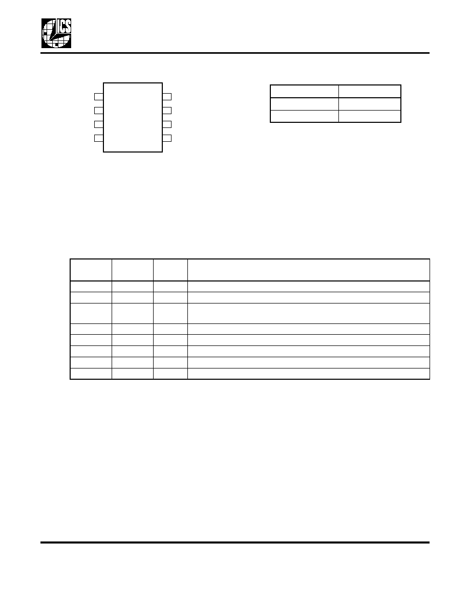
Pin Assignment
40/80M Frequency Selection
* Frequency after power up
Pin Descriptions
External Components
Series Termination Resistor
Clock output traces over one inch should use series
termination. To series terminate a 50
trace (a
commonly used trace impedance), place a 33
resistor
in series with the clock line, as close to the clock output
pin as possible. The nominal impedance of the clock
output is 20
.
Decoupling Capacitor
As with any high performance mixed-signal IC, the
ICS408 must be isolated from system power supply
noise to perform optimally.
A decoupling capacitor of 0.01µF must be connected
between VDD and the PCB ground plane.
Crystal Load Capacitors
The device crystal connections should include pads for
small capacitors from X1 to ground and from X2 to
ground. These capacitors are used to adjust the stray
capacitance of the board to match the nominally
required crystal load capacitance. Because load
capacitance can only be increased in this trimming
process, it is important to keep stray capacitance to a
minimum by using very short PCB traces (and no vias)
1
2
3
X 1
4
V D D
G N D
O E / L A T
2 4 . 5 7 6 M
4 0 / 8 0 M
2 5 M
8
7
6
5
X 2
8 P i n ( 1 5 0 m i l ) S O I C
At Power Up
Pin 3* (40/80)
0
40M
1
80M
Pin
Number
Pin
Name
Pin
Type
Pin Description
1
X1
Input
Crystal connection. Connect to 14.31818 MHz parallel mode crystal.
2
24.576M
Output
24.576 MHz clock output. Tri-state when OE/LAT is low.
3
40/80M
Input/
Output
40M or 80M selectable clock output. Latched on rising edge of
OE/LAT. Tri-state when OE/LAT is low.
4
25M
Output
25 MHz clock output.
5
GND
Power
Connect to ground.
6
VDD
Power
Connect to voltage supply.
7
OE/LAT
Input
Disables or latches 40/80 MHz output.
8
X2
Input
Crystal connection. Connect to 14.31818 MHz parallel mode crystal.

PC P
ERIPHERAL
C
LOCK
MDS 408 B
3
Revision 032602
Integrated Circuit Systems, Inc.
q
525 Race Street, San Jose, CA 95126
q
tel (408) 295-9800
q
www.icst.com
ICS408
been the crystal and device. Crystal capacitors must be
connected from each of the pins X1 and X1 to ground.
The value (in pF) of these crystal caps should equal
(C
L
-6pF)*2. In this equation, C
L
= crystal load
capacitance in pF. Example: For a crystal with a 15 pF
load capacitance, each crystal capacitor would be 18
pF [(15-6) x 2] = 18.
PCB Layout Recommendations
For optimum device performance and lowest output
phase noise, the following guidelines should be
observed.
1) The 0.01µF decoupling capacitor should be mounted
on the component side of the board as close to the
VDD pin as possible. No vias should be used between
the decoupling capacitor and VDD pin. The PCB trace
to VDD pin should be kept as short as possible, as
should the PCB trace to the ground via.
2) The external crystal should be mounted just next to
the device with short traces. The X1 and X2 traces
should not be routed next to each other with minimum
spaces, instead they should be separated and away
from other traces.
3) To minimize EMI the 33
series termination resistor,
if needed, should be placed close to the clock output.
4) An optimum layout is one with all components on the
same side of the board, minimizing vias through other
signal layers. Other signal traces should be routed
away from the ICS408. This includes signal traces just
underneath the device, or on layers adjacent to the
ground plane layer used by the device.
Selection of 40M/80M Clock
The 40/80M output clock is selected by a soft pull-upp
or pull-down on 40/80M pin (pin 3). On power up, the
rising edge on OE latches, in the high or low level, on
pin 3 which starts the appropriate frequency. Any
low-to-high transistion on OE/LAT after power up will
latch the logic level on pin 3.

PC P
ERIPHERAL
C
LOCK
MDS 408 B
4
Revision 032602
Integrated Circuit Systems, Inc.
q
525 Race Street, San Jose, CA 95126
q
tel (408) 295-9800
q
www.icst.com
ICS408
Absolute Maximum Ratings
Stresses above the ratings listed below can cause permanent damage to the ICS408. These ratings, which
are standard values for ICS commercially rated parts, are stress ratings only. Functional operation of the
device at these or any other conditions above those indicated in the operational sections of the
specifications is not implied. Exposure to absolute maximum rating conditions for extended periods can
affect product reliability. Electrical parameters are guaranteed only over the recommended operating
temperature range.
Recommended Operation Conditions
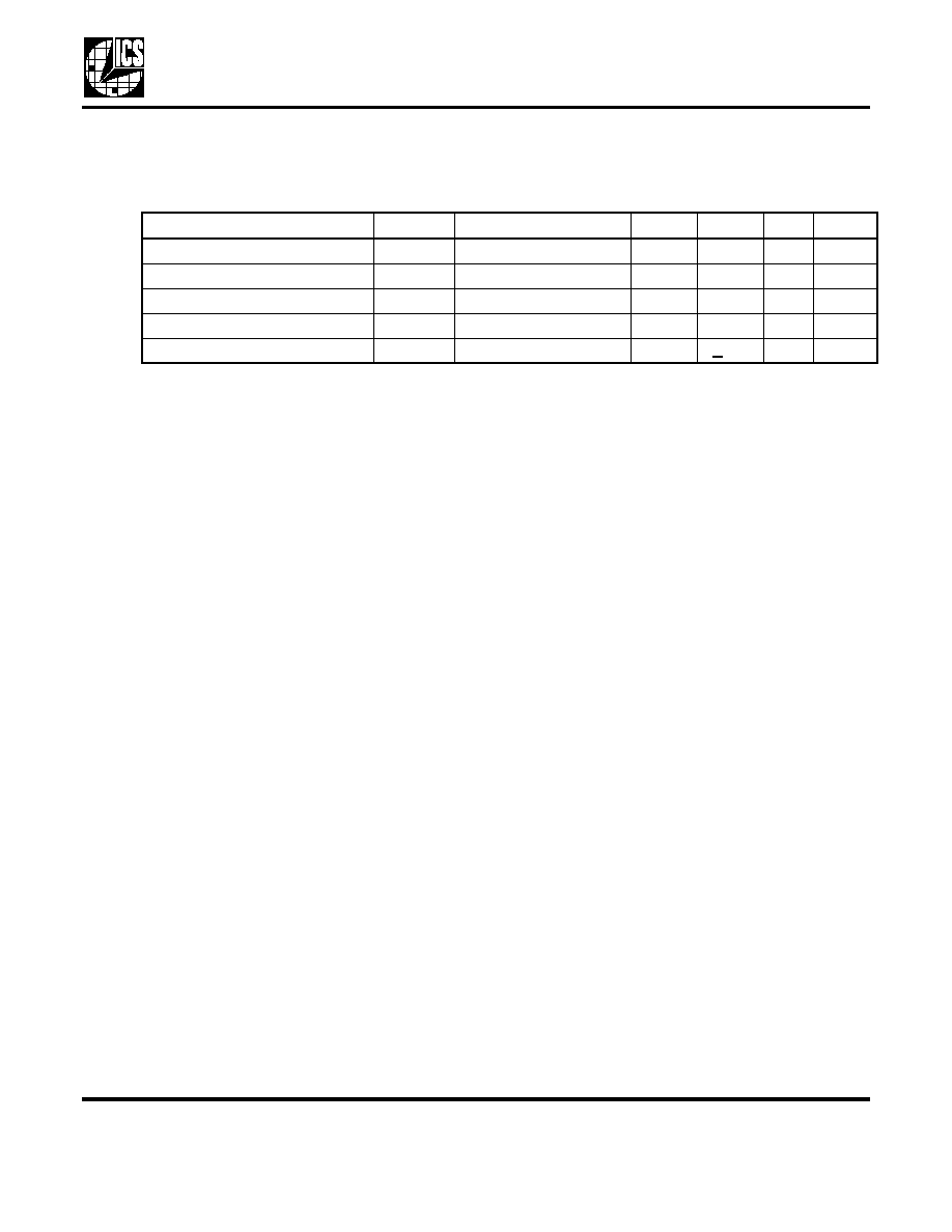
DC Electrical Characteristics
VDD=3.3V
±10%
Item
Rating
Supply Voltage, VDD
7 V
All Inputs and Outputs
-0.5 V to VDD+0.5 V
Ambient Operating Temperature
0 to +70
∞
C
Storage Temperature
-65 to +150
∞
C
Junction Temperature
175
∞
C
Soldering Temperature
260
∞
C
Parameter
Min.
Typ.
Max.
Units
Ambient Operating Temperature
0
≠
+70
∞
C
Power Supply Voltage (measured in respect to GND)
+3.00
+3.60
V
Parameter
Symbol
Conditions
Min.
Typ.
Max.
Units
Operating Voltage
VDD
3.0
3.6
V
Input High Voltage
V
IH
VDD
-
0.5
V
Input Low Voltage
V
IL
0.5
V
Output High Voltage
V
OH
I
OH
= -20 mA
2.4
V
Output Low Voltage
V
OL
I
OL
= 20 mA
0.8
V
Operating Supply Current
IDD
No load on
outputs
15
mA
Short Circuit Current
I
OS
Each output
60
mA
PC P
ERIPHERAL
C
LOCK
MDS 408 B
5
Revision 032602
Integrated Circuit Systems, Inc.
q
525 Race Street, San Jose, CA 95126
q
tel (408) 295-9800
q
www.icst.com
ICS408
AC Electrical Characteristics
VDD = 3.3V ±10%
, Ambient Temperature 0 to +70◊ C
Parameter
Symbol
Conditions
Min.
Typ.
Max.
Units
Input Frequency
14.318
MHz
Output Rise Time
t
OR
0.8 to 2.0 V, C
L
=15 pF
0.8
ns
Output Fall Time
t
OF
2.0 to 0.8 V, C
L
=15 pF
0.6
ns
Output Clock Duty Cycle
at VDD/2
45
50
55
%
Absolute Jitter, Short Term
variation from mean
+250
ps

PC P
ERIPHERAL
C
LOCK
MDS 408 B
6
Revision 032602
Integrated Circuit Systems, Inc.
q
525 Race Street, San Jose, CA 95126
q
tel (408) 295-9800
q
www.icst.com
ICS408
Package Outline and Package Dimensions
(8 pin SOIC, 150 Mil. Narrow Body)
Package dimensions are kept current with JEDEC Publication No. 95
Ordering Information
While the information presented herein has been checked for both accuracy and reliability, Integrated Circuit Systems (ICS)
assumes no responsibility for either its use or for the infringement of any patents or other rights of third parties, which would
result from its use. No other circuits, patents, or licenses are implied. This product is intended for use in normal commercial
applications. Any other applications such as those requiring extended temperature range, high reliability, or other extraordinary
environmental requirements are not recommended without additional processing by ICS. ICS reserves the right to change any
circuitry or specifications without notice. ICS does not authorize or warrant any ICS product for use in life support devices or
critical medical instruments.
Part / Order Number
Marking
Shipping
Packaging
Package
Temperature
ICS408M
ICS408
Tubes
8 pin SOIC
0 to 70
∞
C
ICS408MT
ICS408
Tape and Reel
8 pin SOIC
0 to 70
∞
C
D
E
H
c
h x 4 5
0
b
e
Q
A
P in 1
In d e x
A r e a
Millimeters
Inches
Symbol
Min
Max
Min
Max
A
1.35
1.75
0.0532
0.0688
A1
1.10
0.25
0.0040
0.0098
B
0.33
0.51
0.013
0.020
C
0.19
0.25
0.0075
0.0098
D
4.80
5.00
.1890
.1968
E
3.80
4.00
0.1497
0.1574
e
1.27 Basic
0.050 Basic
H
5.80
6.20
0.2284
0.2440
h
0.25
0.50
0.010
0.020
L
0.40
1.27
0.016
0.050
a
0
∞
8
∞
0
∞
8
∞