 | –≠–ª–µ–∫—Ç—Ä–æ–Ω–Ω—ã–π –∫–æ–º–ø–æ–Ω–µ–Ω—Ç: ICS411M | –°–∫–∞—á–∞—Ç—å:  PDF PDF  ZIP ZIP |
ICS411
MDS 411 C
1
Revision 062005
Integrated Circuit Systems
l
525 Race Street, San Jose, CA 95126
l
tel (408) 297-1201
l
www.icst.com
PC P
ERIPHERAL
C
LOCK
Description
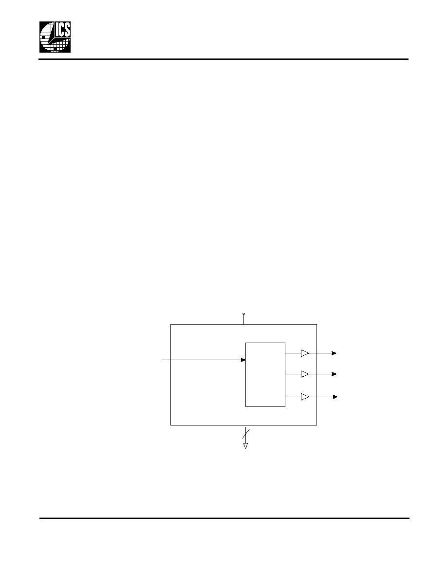
The ICS411 is a cost-effective clock synthesizer
developed to optimize component count for PC
motherboard and peripheral applications. The device
supports a common, low cost 14.31818 MHz crystal.
The device locks all output frequencies to enhance
system performance. By supporting common PC
peripheral interface frequencies including 25 MHz for
Ethernet and 24.576 MHz for audio and other
applications, the device lowers chip count enhancing
system cost and reliability.
The ICS411 utilizes a low pin count 8-pin SOIC
package to optimize board space.
ICS is a leader in low jitter and power consumer
application clock sources. These devices are capable
of supporting CCD, video, audio, USB, CPU, and other
peripherals.
Features
∑
Low operating voltage of 3.3 V
∑
Accepts 14.31818 MHz clock input to lower jitter
∑
Fixed dual 25 MHz clocks for Ethernet
∑
Fixed 24.576 MHz clock
∑
Power consumption of 15 mA (typ) extends battery
life
∑
Duty cycle of 45 to 55% (24.576M)
∑
Packaged in 8-pin SOIC
∑
Available in Pb (lead) free package
∑
Contact ICS for custom frequency requirements
Block Diagram
2 4 .5 7 6 M
IC L K
1 4 .3 1 8 1 8 M H z
P L L
2 5 M
2 5 M
V D D
G N D
2
PC P
ERIPHERAL
C
LOCK
MDS 411 C
2
Revision 062005
Integrated Circuit Systems
l
525 Race Street, San Jose, CA 95126
l
tel (408) 297-1201
l
www.icst.com
ICS411
Pin Assignment
Pin Descriptions
1
2
3
I CL K
4
2 5 M
2 5 M
GND
VDD
GND
2 4 . 5 7 6 M
8
7
6
5
VDD
8 Pi n ( 150 mi l ) SOI C
Pin
Number
Pin
Name
Pin
Type
Pin Description
1
ICLK
Input
Clock connection. Connect to 14.31818 MHz clock.
2
VDD
Power
Connect to voltage supply.
3
GND
Power
Connect to ground.
4
24.576M
Output
24.576 MHz clock output.
5
25M
Output
25 MHz clock output.
6
25M
Output
25 MHz clock output.
7
GND
Power
Connect to ground.
8
VDD
Power
Connect to voltage supply.
PC P
ERIPHERAL
C
LOCK
MDS 411 C
3
Revision 062005
Integrated Circuit Systems
l
525 Race Street, San Jose, CA 95126
l
tel (408) 297-1201
l
www.icst.com
ICS411
External Components
Series Termination Resistor
Clock output traces over one inch should use series
termination. To series terminate a 50
trace (a
commonly used trace impedance), place a 33
resistor
in series with the clock line, as close to the clock output
pin as possible. The nominal impedance of the clock
output is 20
.
Decoupling Capacitor
As with any high performance mixed-signal IC, the
ICS411 must be isolated from system power supply
noise to perform optimally.
Decoupling capacitors of 0.01µF must be connected
between each VDD pin and the PCB ground plane.
PCB Layout Recommendations
For optimum device performance and lowest output
phase noise, the following guidelines should be
observed.
1) 0.01µF decoupling capacitors should be mounted on
the component side of the board as close to the VDD
pin as possible. No vias should be used between
decoupling capacitor and VDD pin. The PCB trace to
VDD pin should be kept as short as possible, as should
the PCB trace to the ground via.
2) To minimize EMI the 33
series termination resistor,
if needed, should be placed close to the clock output.
3) An optimum layout is one with all components on the
same side of the board, minimizing vias through other
signal layers. Other signal traces should be routed
away from the ICS411. This includes signal traces just
underneath the device, or on layers adjacent to the
ground plane layer used by the device.
Absolute Maximum Ratings
Stresses above the ratings listed below can cause permanent damage to the ICS411. These ratings, which
are standard values for ICS commercially rated parts, are stress ratings only. Functional operation of the
device at these or any other conditions above those indicated in the operational sections of the
specifications is not implied. Exposure to absolute maximum rating conditions for extended periods can
affect product reliability. Electrical parameters are guaranteed only over the recommended operating
temperature range.
Recommended Operation Conditions
Item
Rating
Supply Voltage, VDD
7 V
All Inputs and Outputs
-0.5 V to VDD+0.5 V
Ambient Operating Temperature
0 to +70
∞C
Storage Temperature
-65 to +150
∞C
Junction Temperature
125
∞C
Soldering Temperature
260
∞C
Parameter
Min.
Typ.
Max.
Units
Ambient Operating Temperature
0
≠
+70
∞C
Power Supply Voltage (measured in respect to GND)
+3.00
+3.60
V
PC P
ERIPHERAL
C
LOCK
MDS 411 C
4
Revision 062005
Integrated Circuit Systems
l
525 Race Street, San Jose, CA 95126
l
tel (408) 297-1201
l
www.icst.com
ICS411
DC Electrical Characteristics
VDD=3.3 V
±10%
Notes: 1. Nominal switching threshold is VDD/2
AC Electrical Characteristics
VDD = 3.3 V ±10%
, Ambient Temperature 0 to +70∞ C
Parameter
Symbol
Conditions
Min.
Typ.
Max.
Units
Operating Voltage
VDD
3.0
3.6
V
Input High Voltage
V
IH
Note 1
2.0
V
Input Low Voltage
V
IL
Note 1
0.8
V
Output High Voltage
V
OH
I
OH
= -25 mA
2.4
V
Output Low Voltage
V
OL
I
OL
= 25 mA
0.8
V
Operating Supply Current
IDD
No load
8
mA
Short Circuit Current
I
OS
Each output
80
mA
Parameter
Symbol
Conditions
Min.
Typ.
Max. Units
Input Frequency
14.318
MHz
Output Rise Time
t
OR
0.8 to 2.0 V, C
L
=15 pF
0.60
ns
Output Fall Time
t
OF
2.0 to 0.8 V, C
L
=15 pF
0.60
ns
Output Clock Duty Cycle
At VDD/2, 24.576M
45
50
55
%
Absolute Jitter, Short Term
Variation from mean,
24.576M
150
ps
Absolute Jitter, Short Term
Variation from mean,
25M
115
ps
PC P
ERIPHERAL
C
LOCK
MDS 411 C
5
Revision 062005
Integrated Circuit Systems
l
525 Race Street, San Jose, CA 95126
l
tel (408) 297-1201
l
www.icst.com
ICS411
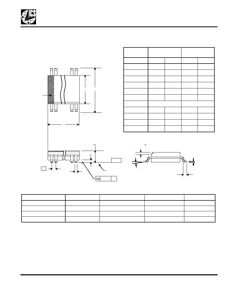
Package Outline and Package Dimensions
(8-pin SOIC, 150 Mil. Narrow Body)
Package dimensions are kept current with JEDEC Publication No. 95
Ordering Information
Parts that are ordered with a "LF" suffix to the part number are the Pb-Free configuration and are RoHS compliant.
While the information presented herein has been checked for both accuracy and reliability, Integrated Circuit Systems (ICS)
assumes no responsibility for either its use or for the infringement of any patents or other rights of third parties, which would
result from its use. No other circuits, patents, or licenses are implied. This product is intended for use in normal commercial
applications. Any other applications such as those requiring extended temperature range, high reliability, or other extraordinary
environmental requirements are not recommended without additional processing by ICS. ICS reserves the right to change any
circuitry or specifications without notice. ICS does not authorize or warrant any ICS product for use in life support devices or
critical medical instruments.
Part / Order Number
Marking
Shipping Packaging
Package
Temperature
ICS411M
ICS411
Tubes
8-pin SOIC
0 to +70
∞C
ICS411MT
ICS411
Tape and Reel
8-pin SOIC
0 to +70
∞C
ICS411MLF
ICS411LF
Tubes
8-pin SOIC
0 to +70
∞C
ICS411MLFT
ICS411LF
Tape and Reel
8-pin SOIC
0 to +70
∞C
INDEX
AREA
1 2
8
D
E
SEATING
PLANE
A1
A
e
- C -
B
.10 (.004)
C
C
L
H
h x 45
*For reference only. Controlling dimensions in mm.
Millimeters
Inches*
Symbol
Min
Max
Min
Max
A
1.35
1.75
.0532
.0688
A1
0.10
0.25
.0040
.0098
B
0.33
0.51
.013
.020
C
0.19
0.25
.0075
.0098
D
4.80
5.00
.1890
.1968
E
3.80
4.00
.1497
.1574
e
1.27 BASIC
0.050 BASIC
H
5.80
6.20
.2284
.2440
h
0.25
0.50
.010
.020
L
0.40
1.27
.016
.050
0
∞
8
∞
0
∞
8
∞