 | ÐлекÑÑоннÑй компоненÑ: ICS508-01 | СкаÑаÑÑ:  PDF PDF  ZIP ZIP |
Untitled Document
MDS 508 D
1
Revision 021103
I n t e g r a t e d C i r cu i t S y st e m s
q
5 2 5 Ra ce S t r e e t , S a n J o s e , C A 9 5 1 2 6
q
t e l ( 4 0 8 ) 2 9 5 - 9 8 0 0
q
w w w. i c s t . c o m
PECL
TO
CMOS C
ONVERTER
ICS508
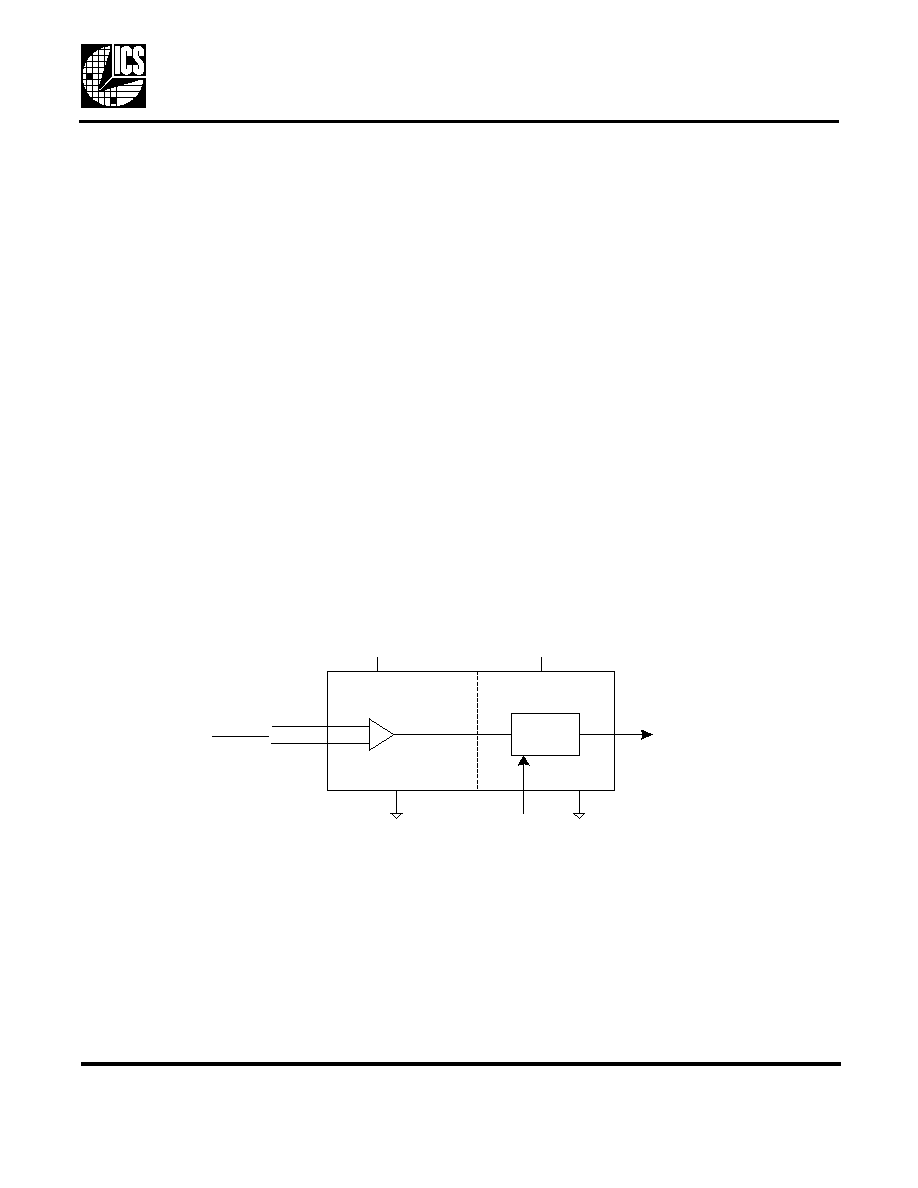
Description
The ICS508 is the most cost effective way to generate
a high quality, high frequency CMOS clock output from
a PECL clock input.
The ICS508 has separate VDD supplies for the PECL
input buffer and the output buffer, allowing different
voltages to be used. For example, the input clock could
use a 3.3 V supply while the output operates from 2.5V.
The device has an Output Enable pin that tri-states the
clock output when the OE pin is taken low.
The ICS508 is a member of ICS' ClockBlocks
TM
family.
Features
·
Packaged in 8 pin SOIC or die
·
Separate VDD supplies allow voltage translation
·
Clock frequency of 0 - 250 MHz
·
Duty cycle of 45/55
·
Operating voltages of 2.375 to 5.5V
·
Tri-state output for board level testing
·
24mA output drive capability
·
Industrial temperature version available
·
Advanced, low power, sub-micron CMOS process
Block Diagram
C LK
O utput
B uffer
V D D C
V D D P
G N D
G N D
O E
P E C LIN
P E C LIN
PECL
TO
CMOS C
ONVERTER
MDS 508 D
2
Revision 021103
I n t e g r a t e d C i r c u i t S y s t e ms
q
5 2 5 R a c e S t r e e t , S a n J o s e , CA 9 5 1 2 6
q
t e l ( 4 0 8 ) 2 9 5 - 9 8 0 0
q
w w w. ic s t . c o m
ICS508
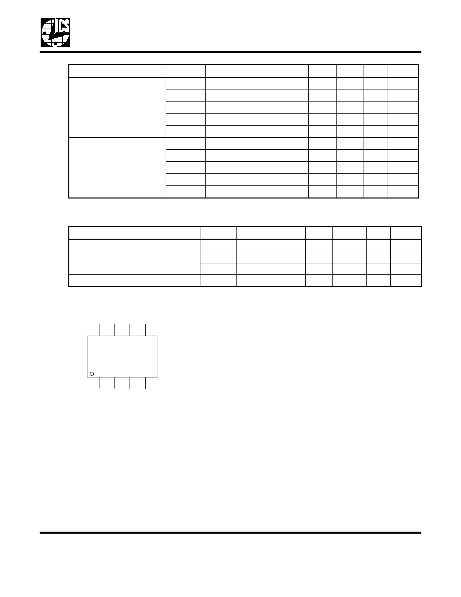
Pin Assignment
Pin Descriptions
External Components
The ICS508 requires two 0.01
µ
F decoupling capacitors to be connected between VDDP and GND and
between VDDC and GND. They must be connected close to the ICS508 to minimize lead inductance. A
33
series terminating resistor can be used next to the CLK pin.
V D D P
P E C L I N
P E C L I N
C L K
G N D
G N D
O E
V D D C
1
2
3
4
8
7
6
5
8 P i n ( 1 5 0 m i l ) S O I C
Pin
Number
Pin
Name
Pin
Type
Pin Description
1
VDDP
Output
Connect to 3.3V or 5V. Supplies PECL input buffer.
2
PECLIN
Input
Complementary PECL clock input.
3
PECLIN
Input
PECL clock input.
4
GND
Power
Connect to ground.
5
OE
Input
Output enable. Tri-states CLK output when low. Internal pull-up to
VDDC.
6
GND
Power
Connect to ground.
7
CLK
Output
Clock output.
8
VDDC
Power
Connect to 2.5V, or 3.3V, or 5V. Supplies output buffer and OE pin.
PECL
TO
CMOS C
ONVERTER
MDS 508 D
3
Revision 021103
I n t e g r a t e d C i r c u i t S y s t e ms
q
5 2 5 R a c e S t r e e t , S a n J o s e , CA 9 5 1 2 6
q
t e l ( 4 0 8 ) 2 9 5 - 9 8 0 0
q
w w w. ic s t . c o m
ICS508
Absolute Maximum Ratings
Stresses above the ratings listed below can cause permanent damage to the ICS508. These ratings, which
are standard values for ICS commercially rated parts, are stress ratings only. Functional operation of the
device at these or any other conditions above those indicated in the operational sections of the
specifications is not implied. Exposure to absolute maximum rating conditions for extended periods can
affect product reliability. Electrical parameters are guaranteed only over the recommended operating
temperature range.
Recommended Operation Conditions
DC Electrical Characteristics
VDDP = VDDC =3.3V ±5%
, Ambient temperature 0 to +70
°
C, unless stated otherwise
Item
Rating
Supply Voltage, VDDP and VDDC
7V
PECL Inputs
-0.5V to VDDP+0.5V
Clock Output and OE Pin
-0.5V to VDDC+0.5V
Ambient Operating Temperature, ICS508
0 to +70
°
C
Ambient Operating Temperature, ICS508MI
-40 to +85
°
C
Storage Temperature
-65 to +150
°
C
Soldering Temperature
260
°
C
Parameter
Min.
Typ.
Max.
Units
Ambient Operating Temperature, ICS508M
0
+70
°
C
Ambient Operating Temperature, ICS508MI
-40
+85
°
C
Power Supply Voltage (measured in respect to GND)
+3.15
+3.45
V
Reference crystal parameters
Refer to page 3
Parameter
Symbol
Conditions
Min.
Typ.
Max.
Units
Operating Voltage
VDD
VDDP
3
5.5
V
VDD
VDDC
2.375
5.5
V
Peak to Peak Input Voltage
PECLIN
0.3
1
V
Common Mode Range
PECLIN
VDDP = 5V
VDDP - 3.7
VDDP - 0.6
V
PECLIN
VDDP = 3.3V
VDDP - 2.0
VDDP - 0.6
V
Input High Voltage
V
IH
OE only
2
VDDC
V
Input Low Voltage
V
IL
OE only
0.8
V
PECL
TO
CMOS C
ONVERTER
MDS 508 D
4
Revision 021103
I n t e g r a t e d C i r c u i t S y s t e ms
q
5 2 5 R a c e S t r e e t , S a n J o s e , CA 9 5 1 2 6
q
t e l ( 4 0 8 ) 2 9 5 - 9 8 0 0
q
w w w. ic s t . c o m
ICS508
Note 1: VDDP must always be greater than or equal to VDDC
AC Electrical Characteristics
VDDP = VDDC = 3.3V±5%
, Ambient Temperature 0 to +70
°
C, unless stated otherwise
Output High Voltage
V
OH
VDDC = 5V
IOH = -24 mA
VDDC - 0.4
V
VDDC = 3.3V
IOH = -18 mA
VDDC - 0.4
V
VDDC = 2.5V
IOH = -8 mA
VDDC - 0.4
V
Output Low Voltage
V
OL
VDDC = 5V
IOL = 24 mA
0.4
V
VDDC = 3.3V
IOL = 18 mA
0.4
V
VDDC = 2.5V
IOL = 8 mA
0.4
V
On Chip Pull-up Resistor
R
PU
OE
250
k
Operating Supply Current
IDDP
100 MHz, no load
1.5
mA
IDDC
100 MHz, no load
8
mA
Parameter
Symbol
Conditions
Min.
Typ.
Max.
Units
Input Frequency
f
IN
0
250
MHz
Output Clock Rise Time
0.8V to 2.0V, VDDC = 5V
0.4
ns
0.8V to 2.0V, VDDC = 3.3V
0.6
ns
0.8V to 2.0V, VDDC = 2.5V
1
ns
Output Clock Fall Time
2.0V to 0.8V, VDDC = 5V
0.4
ns
2.0V to 0.8V, VDDC = 5V
0.6
ns
2.0V to 0.8V, VDDC = 5V
1
ns
Output Enable Time
OE high to output on
7
20
ns
Output Disable Time
OE low to tri-state
7
20
ns
Propagation Delay
VDDP = 5V, VDDC = 5V
4
6
ns
VDDP = 5V, VDDC = 3.3V
4.5
7
ns
VDDP = 5V, VDDC = 2.5V
5.5
9
ns
VDDP = 3.3V, VDDC = 3.3V
4.5
7
ns
VDDP = 3.3V, VDDC = 2.5V
5.5
9
ns
Output Clock Duty Cycle
0 - 100 MHz
Any VDD combination
45
55
%
Parameter
Symbol
Conditions
Min.
Typ.
Max.
Units
PECL
TO
CMOS C
ONVERTER
MDS 508 D
5
Revision 021103
I n t e g r a t e d C i r c u i t S y s t e ms
q
5 2 5 R a c e S t r e e t , S a n J o s e , CA 9 5 1 2 6
q
t e l ( 4 0 8 ) 2 9 5 - 9 8 0 0
q
w w w. ic s t . c o m
ICS508
Thermal Characteristics
Marking Diagram
Notes:
1. ###### is the lot number
2. YYWW is the last two digits of the year and the week number that the part was assembled
Output Clock Duty Cycle
100 - 166 MHz
VDDP = 5V, VDDC = 5V
45
55
%
VDDP = 5V, VDDC = 3.3V
45
55
%
VDDP = 5V, VDDC = 2.5V
40
60
%
VDDP = 3.3V, VDDC = 3.3V
40
60
%
VDDP = 3.3V, VDDC = 2.5V
45
55
%
Output Clock Duty Cycle
166 - 250 MHz
VDDP = 5V, VDDC = 5V
40
60
%
VDDP = 5V, VDDC = 3.3V
40
60
%
VDDP = 5V, VDDC = 2.5V
35
65
%
VDDP = 3.3V, VDDC = 3.3V
35
65
%
VDDP = 3.3V, VDDC = 2.5V
40
60
%
Parameter
Symbol
Conditions
Min.
Typ.
Max.
Units
Thermal Resistance Junction to
Ambient
JA
Still air
150
°
C/W
JA
1 m/s air flow
140
°
C/W
JA
3 m/s air flow
120
°
C/W
Thermal Resistance Junction to Case
JC
40
°
C/W
Parameter
Symbol
Conditions
Min.
Typ.
Max.
Units
ICS508M
######
YYW W
PECL
TO
CMOS C
ONVERTER
MDS 508 D
6
Revision 021103
I n t e g r a t e d C i r c u i t S y s t e ms
q
5 2 5 R a c e S t r e e t , S a n J o s e , CA 9 5 1 2 6
q
t e l ( 4 0 8 ) 2 9 5 - 9 8 0 0
q
w w w. ic s t . c o m
ICS508
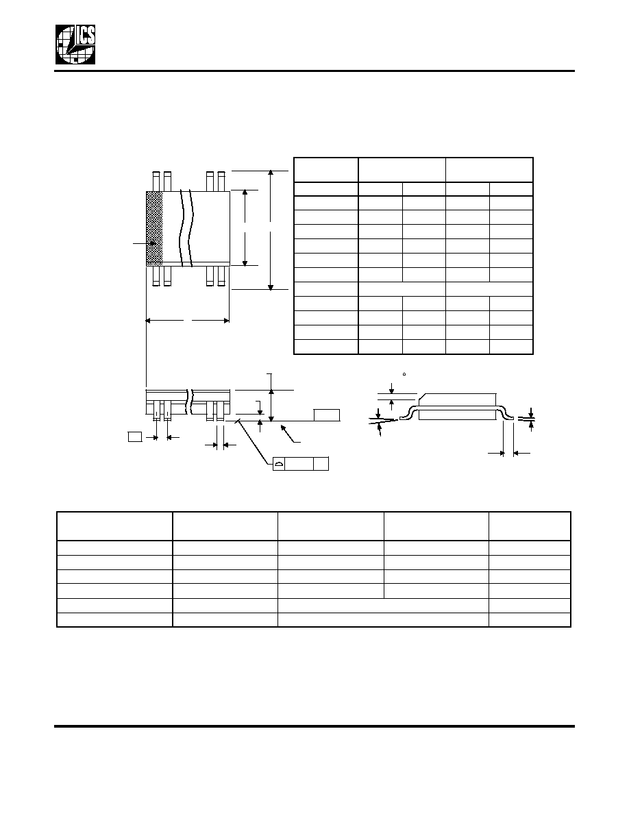
Package Outline and Package Dimensions (8 pin SOIC, 150 Mil. Narrow Body)
Package dimensions are kept current with JEDEC Publication No. 95
Ordering Information
While the information presented herein has been checked for both accuracy and reliability, Integrated Circuit Systems (ICS) assumes no
responsibility for either its use or for the infringement of any patents or other rights of third parties, which would result from its use. No other
circuits, patents, or licenses are implied. This product is intended for use in normal commercial applications. Any other applications such as
those requiring extended temperature range, high reliability, or other extraordinary environmental requirements are not recommended without
additional processing by ICS. ICS reserves the right to change any circuitry or specifications without notice. ICS does not authorize or warrant
any ICS product for use in life support devices or critical medical instruments.
Part / Order Number
Marking
Shipping
packaging
Package
Temperature
ICS508M
ICS508M
Tubes
8 pin SOIC
0 to +70
°
C
ICS508MT
ICS508M
Tape and Reel
8 pin SOIC
0 to +70
°
C
ICS508MI
ICS508I
Tubes
8 pin SOIC
-40 to +85
°
C
ICS508MIT
ICS508I
Tape and Reel
8 pin SOIC
-40 to +85
°
C
ICS508-DWF
-
Die on uncut, probed wafers
0 to +70
°
C
ICS508-DPK
-
Tested die in waffle pack
0 to +70
°
C
INDEX
AREA
1 2
8
D
E
SEATING
PLANE
A1
A
e
- C -
B
.10 (.004)
C
C
L
H
h x 45
Millimeters
Inches
Symbol
Min
Max
Min
Max
A
1.35
1.75
.0532
.0688
A1
0.10
0.25
.0040
.0098
B
0.33
0.51
.013
.020
C
0.19
0.25
.0075
.0098
D
4.80
5.00
.1890
.1968
E
3.80
4.00
.1497
.1574
e
1.27 BASIC
0.050 BASIC
H
5.80
6.20
.2284
.2440
h
0.25
0.50
.010
.020
L
0.40
1.27
.016
.050
0
°
8
°
0
°
8
°
Document Outline