 | –≠–ª–µ–∫—Ç—Ä–æ–Ω–Ω—ã–π –∫–æ–º–ø–æ–Ω–µ–Ω—Ç: ICS513 | –°–∫–∞—á–∞—Ç—å:  PDF PDF  ZIP ZIP |

ICS513
LOCOTM PLL Clock Generator
MDS 513 B
1
Revision 080699
Printed 12/4/00
Integrated Circuit Systems ∑ 525 Race Street ∑ San Jose ∑ CA∑ 95126 ∑ (408)295-9800tel∑ (408)295-9818fax
∑ Packaged as 8 pin SOIC
∑ ICS' lowest cost PLL clock plus reference
∑ Produces common computer frequencies
∑ Input crystal frequency typically 14.3182 MHz
∑ Output clock frequencies up to 100 MHz
∑ Low jitter - 40 ps one sigma
∑ Compatible with all popular CPUs
∑ Duty cycle of 45/55
∑ Custom frequencies available
∑ Operating voltages of 3.0 to 5.5 V
∑ Power down mode turns off chip
∑ 25mA drive capability at TTL levels
∑ Advanced, low power CMOS process
The ICS513 LOCOTM is the most cost effective
way to generate a high quality, high frequency
clock output from a 14.31818 MHz crystal or
clock input. The name LOCO stands for LOw
Cost Oscillator, as it is designed to replace crystal
oscillators in many electronic systems. Using
Phase-Locked-Loop (PLL) techniques, the device
uses a standard, inexpensive crystal to produce
output clocks up to 100 MHz.
Stored in the chip's ROM is the ability to generate
5 different output frequencies, allowing one chip
to work in different speed processor systems.
The device also has a power down mode that turns
off the clock outputs when both select pins are low.
In this mode, the internal PLL is not running.
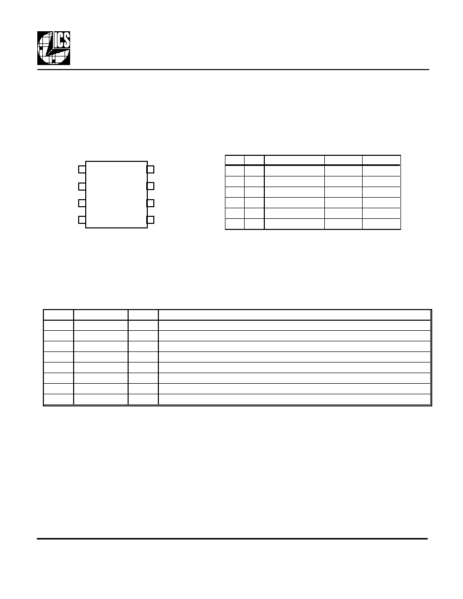
Block Diagram
Description
Features
CLK
Crystal
Oscillator
VDD GND
PLL
Clock
Synthesis
and Control
Circuitry
Output
Buffer
14.31818 MHz
crystal
or clock
REF
X2
X1/ICLK
Output
Buffer
S1, S0
2
Optional crystal capacitors
ICS513
LOCOTM PLL Clock Generator
MDS 513 B
2
Revision 080699
Printed 12/4/00
Integrated Circuit Systems ∑ 525 Race Street ∑ San Jose ∑ CA∑ 95126 ∑ (408)295-9800tel∑ (408)295-9818fax
S1
S0
CLK
Multiplier
Accuracy
0
0
Power Down CLK
-
-
0
1
100
6.984
1 ppm
M
0
24
1.676
1 ppm
M
1
14.31818
1
0 ppm
1
0
48
3.353
0.017%
1
1
3.6864
0.2576
0.044%
Pin Assignment
1
8
2
3
4
7
6
5
X1/ICLK
VDD
GND
REF
X2
S1
S0
CLK
Number
Name
Type
Description
1
X1/ICLK
I
Crystal connection to 14.31818 MHz crystal or clock input.
2
VDD
P
Connect to +3.3 V or +5 V.
3
GND
P
Connect to ground.
4
REF
O
Reference 14.31818 MHz crystal oscillator buffered clock output.
5
CLK
O
Clock output per table above.
6
S0
TI
Select 0 for output clock. Connect to GND or VDD or float. See table above.
7
S1
TI
Select 1 for output clock. Connect to GND or VDD or float. See table above.
8
X2
O
Crystal connection to 14.31818 MHz crystal. Leave unconnected for clock input.
Pin Descriptions
Key: I = Input, TI = Tri-Level Input, O = output, P = power supply connection
Clock Decoding Table (MHz) with
14.31818MHz Crystal or Clock Input
0 = connect directly to ground.
1 = connect directly to VDD.
M = leave unconnected (floating).
CLK and REF stop low in power down state.
Notes: 1. With S1 = S0 = 0, the internal PLL is turned off and the CLK output stops low.
The crystal oscillator and REF output are still active.
2. With a clock input, the phase relationship between the input and output clocks can change
each time the device is powered on.
If a fixed phase relationship is required, please use our ICS571 or other zero delay multiplier.
ICS513
LOCOTM PLL Clock Generator
MDS 513 B
3
Revision 080699
Printed 12/4/00
Integrated Circuit Systems ∑ 525 Race Street ∑ San Jose ∑ CA∑ 95126 ∑ (408)295-9800tel∑ (408)295-9818fax
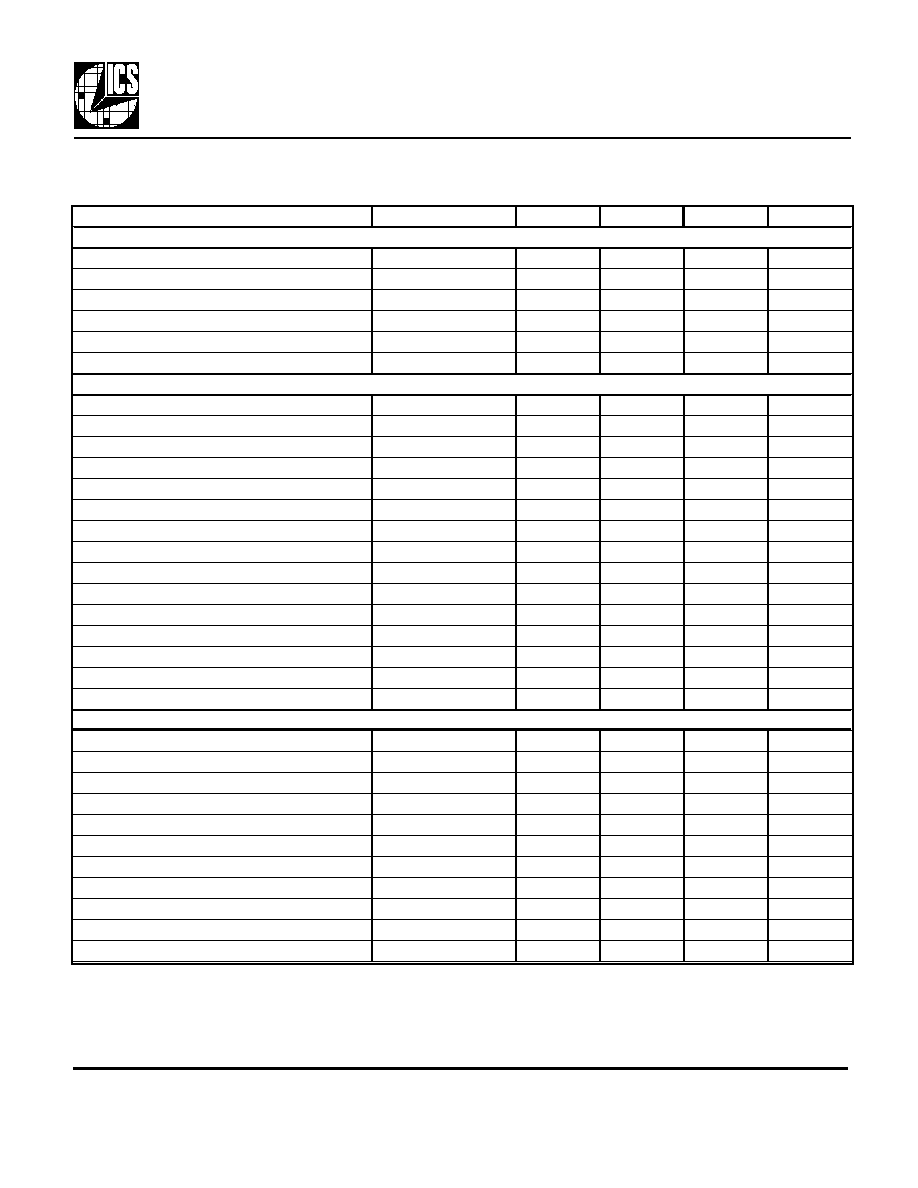
Electrical Specifications
Parameter
Conditions
Minimum
Typical
Maximum
Units
ABSOLUTE MAXIMUM RATINGS (stresses beyond these can permanently damage the device)
ABSOLUTE MAXIMUM RATINGS (stresses beyond these can permanently damage the device)
ABSOLUTE MAXIMUM RATINGS (stresses beyond these can permanently damage the device)
ABSOLUTE MAXIMUM RATINGS (stresses beyond these can permanently damage the device)
Supply Voltage, VDD
Referenced to GND
7
V
Inputs
Referenced to GND
-0.5
VDD+0.5
V
Clock Output
Referenced to GND
-0.5
VDD+0.5
V
Ambient Operating Temperature
0
70
∞C
Soldering Temperature
Max of 10 seconds
260
∞C
Storage temperature
-65
150
∞C
DC CHARACTERISTICS (VDD = 5.0 V unless otherwise noted)
DC CHARACTERISTICS (VDD = 5.0 V unless otherwise noted)
Operating Voltage, VDD
3
5.5
V
Input High Voltage, VIH, ICLK only
ICLK (Pin 1)
(VDD/2)+1
VDD/2
V
Input Low Voltage, VIL, ICLK only
ICLK (Pin 1)
VDD/2
(VDD/2)-1
V
Input High Voltage, VIH
S0
2
V
Input Low Voltage, VIL
S0
0.8
V
Input High Voltage, VIH
S1
VDD-0.5
V
Input Low Voltage, VIM
S1
VDD/2
V
Input Low Voltage, VIL
S1
0.5
V
Output High Voltage, VOH
IOH=-25mA
2.4
V
Output Low Voltage, VOL
IOL=25mA
0.4
V
IDD Operating Supply Current
No Load, 100 MHz
20
mA
IDD Power Down Supply Current, 3.3 V
S1 = S0 = 0
1.5
mA
Short Circuit Current
CLK output
±70
mA
On-Chip Pull-up Resistor
Pin 6
270
k
Input Capacitance, S1, S0
Pins 6, 7
4
pF
AC CHARACTERISTICS (VDD = 5.0V unless otherwise noted)
AC CHARACTERISTICS (VDD = 5.0V unless otherwise noted)
Input Frequency, crystal input
5
14.31818
27
MHz
Input Frequency, clock input
2
14.31818
50
MHz
Output Frequency
VDD = 4.5 to 5.5 V
14
100
140
MHz
Output Frequency
VDD = 3.0 to 3.6 V
14
100
100
MHz
Output Clock Rise Time
0.8 to 2.0V
1
ns
Output Clock Fall Time
2.0 to 0.8V
1
ns
Output Clock Duty Cycle
1.5V, up to 140 MHz
45
49 to 51
55
%
Power up time, from PD to outputs stable
5
10
ms
Power down time, from running to PD state
50
ns
Absolute Clock Period Jitter
Deviation from mean
±110
ps
One Sigma Clock Period Jitter
40
ps

ICS513
LOCOTM PLL Clock Generator
MDS 513 B
4
Revision 080699
Printed 12/4/00
Integrated Circuit Systems ∑ 525 Race Street ∑ San Jose ∑ CA∑ 95126 ∑ (408)295-9800tel∑ (408)295-9818fax
While the information presented herein has been checked for both accuracy and reliability, Integrated Circuit Systems, Incorporated (ICS) assumes no responsibility for either its
use or for the infringement of any patents or other rights of third parties, which would result from its use. No other circuits, patents, or licenses are implied. This product is
intended for use in normal commercial applications. Any other applications such as those requiring extended temperature range, high reliability, or other extraordinary
environmental requirements are not recommended without additional processing by ICS. ICS reserves the right to change any circuitry or specifications without notice. ICS does
not authorize or warrant any ICS product for use in life support devices or critical medical instruments.
Package Outline and Package Dimensions
Inches
Inches
Millimeters
Millimeters
Symbol
Min
Max
Min
Max
A
0.055
0.068
1.397
1.7272
b
0.013
0.019
0.330
0.483
D
0.185
0.200
4.699
5.080
E
0.150
0.160
3.810
4.064
H
0.225
0.245
5.715
6.223
e .050 BSC
.050 BSC
1.27 BSC
1.27 BSC
h
0.015
0.381
L
0.016
0.035
0.406
0.889
Q
0.004
0.01
0.102
0.254
8 pin SOIC
Ordering Information
Part/Order Number
Marking
Package
Temperature
ICS513M
ICS513M
8 pin SOIC
0-70∞C
ICS513MT
ICS513M
8 pin SOIC on tape and reel
0-70∞C
External Components / Crystal Selection
The ICS513 requires a 0.01µF decoupling capacitor to be connected between VDD and GND. It must be
connected close to the ICS513 to minimize lead inductance. No external power supply filtering is required
for this device. A 33
terminating resistor can be used next to the CLK and REF pins. The total on-chip
capacitance is approximately 12 pF, so a parallel resonant, fundamental mode crystal should be used. For
crystals with a specified load capacitance greater than 12 pF, crystal capacitors should be connected from
each of the pins X1 and X2 to Ground as shown in the Block Diagram on page 1. The value (in pF) of
these crystal caps should be = (CL-12)*2, where CL is the crystal load capacitance in pF. These external
capacitors are only required for applications where the exact frequency is critical. For a clock input,
connect to X1 and leave X2 unconnected (no capacitors on either).
c
A
b
D
E
H
e
h x 45∞
Q
Pin 1
LOCO is a trademark of ICS
L