ICS525-07/08
MDS 525-07/08 A
1
Revision 101105
Integrated Circuit Systems, Inc.
525 Race Street, San Jose, CA 95126
tel (408) 297-1201
www.icst.com
LVCMOS User Configurable Clock
PRELIMINARY INFORMATION
Description
The ICS525-07/08 are the most flexible way to
generate a high-quality clock output from an
inexpensive crystal or clock input at low supply
voltages. The user can configure the device to produce
nearly any output frequency from any input frequency
by grounding or floating the select pins or by driving or
hard wiring the select pins high or low. Neither
microcontroller, software, nor device programmer are
needed to set the frequency. Using Phase-Locked
Loop (PLL) techniques, the device accepts a standard
fundamental mode, inexpensive crystal to produce
output clocks up to 250 MHz. It can also produce a
highly accurate output clock from a given input clock,
keeping them frequency locked.
For similar capability with a serial interface, use the
ICS307.
This product is intended for clock generation. It has low
output jitter (variation in the output period), but input to
output skew is not defined nor guaranteed.
Features
∑
Packaged as 28-pin SSOP (150 mil body)
∑
Available in Pb (lead) free package
∑
User determines the output frequency by setting all
internal dividers
∑
Eliminates need for custom oscillators
∑
Low voltage operation
∑
Pull-ups on all select inputs
∑
Input crystal frequency of 5 - 27 MHz
∑
Input clock frequency of 2 - 50 MHz
∑
Compensated loop bandwidth
∑
Enhanced low frequency operation (-08 version)
∑
Low jitter
∑
Duty cycle of 45/55 up to 200 MHz
∑
Operating voltage of 1.8 V to 2.5 V
∑
Ideal for oscillator replacement
∑
Available in commercial and industrial temperature
ranges
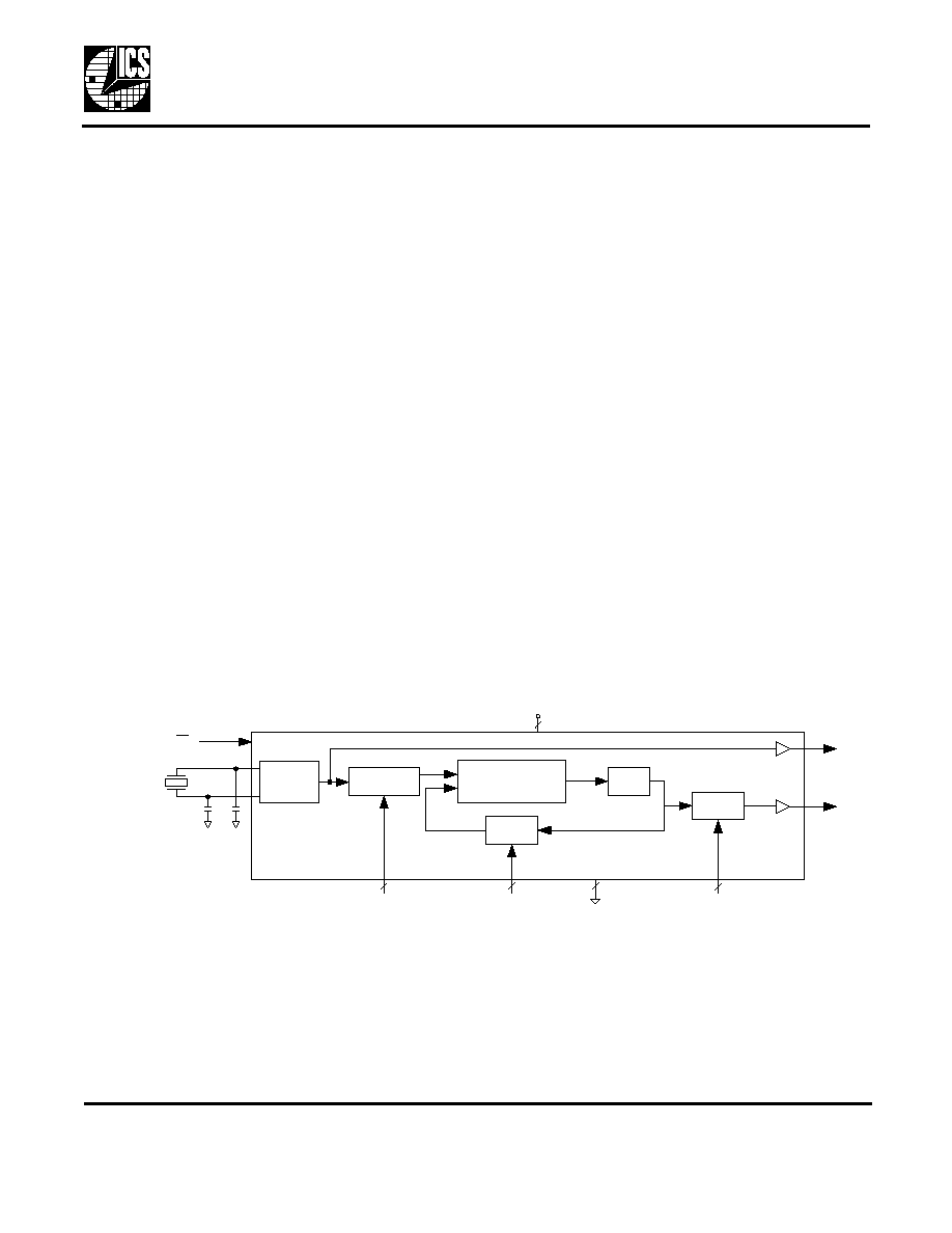
Block Diagram
VDD
GND
2
2
CLK
REF
Reference
Divider
Phase Comparator,
Charge Pump, and
Loop Filter
VCO
VCO
Divider
Output
Divider
R Configuration Pins
V Configuration Pins
S Configuration Pins
X1/ICLK
X2
Crystal or clock
input
Optional crystal capacitors
Crystal
Oscillator
PD
VDD
GND
2
2
CLK
REF
Reference
Divider
Phase Comparator,
Charge Pump, and
Loop Filter
VCO
VCO
Divider
Output
Divider
R Configuration Pins
V Configuration Pins
S Configuration Pins
X1/ICLK
X2
Crystal or clock
input
Optional crystal capacitors
Crystal
Oscillator
PD

LVCMOS User Configurable Clock
MDS 525-07/08 A
2
Revision 101105
Integrated Circuit Systems, Inc.
525 Race Street, San Jose, CA 95126
tel (408) 297-1201
www.icst.com
ICS525-07/08
PRELIMINARY INFORMATION
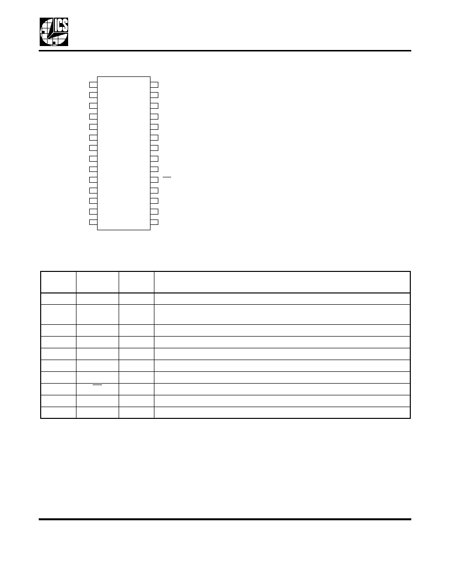
Pin Assignment (ICS525-07)
Pin Descriptions (ICS525-07)
KEY: I(PU) = Input with internal pull-up resistor; X1, X2 = crystal connections
18
7
17
8
16
9
15
X1/ICLK
10
X2
11
GND
12
CLK
13
V0
14
V1
GND
PD
V8
V2
V7
V5
V3
V6
22
21
20
19
V4
REF
5
6
S2
VDD
VDD
24
23
R0
3
4
S0
S1
R1
26
25
R2
1
2
R5
R6
R3
28
27
R4
Pin
Number
Pin
Name
Pin
Type
Pin Description
1, 2,
24-28
R5, R6,
R0-R4
I(PU)
Reference divider word input pins.
3, 4, 5
S0, S1, S2
I(PU)
Select pins for output divider. See table on page 4.
6, 23
VDD
Power
Connect to VDD.
7
X1/ICLK
X1
Crystal connection. Connect to a parallel resonant fundamental crystal or input clock.
8
X2
X2
Crystal connection. Connect to a crystal or leave unconnected for clock.
9, 20
GND
Power
Connect to ground.
10 - 18
V0 - V8
I(PU)
VCO divider word input pins.
19
PD
Input
Power-down. Active low. Turns off entire chip when low. Clock outputs stop low.
21
CLK
Output
PLL output clock.
22
REF
Output
Reference output. Buffered crystal oscillator (or clock) output.
LVCMOS User Configurable Clock
MDS 525-07/08 A
3
Revision 101105
Integrated Circuit Systems, Inc.
525 Race Street, San Jose, CA 95126
tel (408) 297-1201
www.icst.com
ICS525-07/08
PRELIMINARY INFORMATION
Pin Assignment (ICS525-08)
Pin Descriptions (ICS525-08)
18
7
17
8
16
9
15
X1/ICLK
10
X2
11
GND
12
CLK
13
V0
14
V1
GND
PD
V8
V2
V7
V5
V3
V6
22
21
20
19
V4
REF
5
6
S2
VDD
VDD
24
23
R0
3
4
S0
S1
R1
26
25
R2
1
2
R5
S3
R3
28
27
R4
Pin
Number
Pin
Name
Pin
Type
Pin Description
1, 24-28
R5, R0-R4
I(PU)
Reference divider word input pins.
2, 3, 4, 5
S0, S1, S2,
S3
I(PU)
Select pins for output divider. See table on page 4.
6, 23
VDD
Power
Connect to VDD.
7
X1/ICLK
X1
Crystal connection. Connect to a parallel resonant fundamental crystal or input clock.
8
X2
X2
Crystal connection. Connect to a crystal or leave unconnected for clock.
9, 20
GND
Power
Connect to ground.
10 - 18
V0 - V8
I(PU)
VCO divider word input pins.
19
PD
Input
Power-down. Active low. Turns off entire chip when low. Clock outputs stop low.
21
CLK
Output
PLL output clock.
22
REF
Output
Reference output. Buffered crystal oscillator (or clock) output.

LVCMOS User Configurable Clock
MDS 525-07/08 A
4
Revision 101105
Integrated Circuit Systems, Inc.
525 Race Street, San Jose, CA 95126
tel (408) 297-1201
www.icst.com
ICS525-07/08
PRELIMINARY INFORMATION
Output Frequency and Output Divider Table (ICS525-07)
Output Frequency and Output Divider Table (ICS525-08)
S2
Pin 5
S1
Pin 4
S0
Pin 3
CLK Output
Divider
Output Frequency Range (MHz)
VDD = 2.5 V
VDD = 1.8 V
Min
Max
Min
Max
0
0
0
12
8.3
20.8
8.3
20.8
0
0
1
2
50
125
50
125
0
1
0
16
6.25
15.63
6.25
15.63
0
1
1
4
25
62.5
25
62.5
1
0
0
5
20
50
20
50
1
0
1
7
14.3
35.7
14.3
35.7
1
1
0
1
100
250
100
250
1
1
1
3
33.3
83.33
33.3
83.33
S3
Pin 2
S2
Pin 5
S1
Pin 4
S0
Pin 3
CLK Output
Divider
Output Frequency Range (MHz)
VDD = 2.5 V
VDD = 1.8 V
Min
Max
Min
Max
0
0
0
0
2
23.9
200
23.9
200
0
0
0
1
3
15.9
200
15.9
200
0
0
1
0
4
11.9
200
11.9
200
0
0
1
1
5
9.5
158.4
9.5
158.4
0
1
0
0
7
6.8
113.1
6.8
113.1
0
1
0
1
8
6.0
99.0
6.0
99.0
0
1
1
0
9
5.3
88.0
5.3
88.0
0
1
1
1
10
4.8
79.2
4.8
79.2
1
0
0
0
11
4.3
72.0
4.3
72.0
1
0
0
1
13
3.7
60.9
3.7
60.9
1
0
1
0
14
3.4
56.6
3.4
56.6
1
0
1
1
15
3.2
52.8
3.2
52.8
1
1
0
0
17
2.8
46.6
2.8
46.6
1
1
0
1
19
2.5
41.7
2.5
41.7
1
1
1
0
48
1.0
16.5
1.0
16.5
1
1
1
1
128
0.4
6.2
0.4
6.2

LVCMOS User Configurable Clock
MDS 525-07/08 A
5
Revision 101105
Integrated Circuit Systems, Inc.
525 Race Street, San Jose, CA 95126
tel (408) 297-1201
www.icst.com
ICS525-07/08
PRELIMINARY INFORMATION
External Components/Crystal
Selection
Decoupling Capacitors
The ICS525-07/08 require two 0.01ĶF decoupling
capacitors to be connected between VDD and GND,
one on each side of the chip. The capacitor must be
connected close to the device to minimize lead
inductance.
Crystal Load Capacitors
The approximate total on-chip capacitance for a crystal
is 16 pF, so a parallel resonant, fundamental mode
crystal with this value of load (correlation) capacitance
should be used. For crystals with a specified load
capacitance greater than 16 pF, crystal capacitors may
be connected from each of the pins X1 and X2 to
Ground as shown in the block diagram. The value (in
pF) of these crystal caps should be (CL -16)*2, where
CL is the crystal load capacitance in pF. These external
capacitors are only required for applications where the
exact frequency is critical. For a clock input, connect to
X1 and leave X2 unconnected (no capacitors on
either).
Configuring the Frequency
The ICS525-07/08 output frequency is determined by
its internal dividers according to this equation:
V is the feedback divider and can be 8, 9, 10, 12...519
(not 11).
For the ICS525-07, R is the reference divider and can
be 2, 3, 4...129.
For the ICS525-08, R can be 1, 2...64.
For the ICS525-07, OD can be 1, 2, 3, 4, 5, 7, 12, or 16.
For the ICS525-08, OD can be 2, 3, 4, 5, 7, 8, 9, 10, 11,
13, 14, 15, 17, 19, 48, or 128.
The VCO must be kept in its operating range according
to this equation:
The phase detector must be kept in its operating range
according to this equation:
Optimum values for V, R, and OD are found iteratively
by applying the above equations. Choosing a smaller
value of R will give better jitter. A calculator program is
available on the ICS website to automate the process.
After determining V, R, and OD, convert them to the pin
address.
V8...0 = binary(V - 8)
Example: V = 17, V8...0 = 000001001
For the ICS525-07, R6...0 = binary(R - 2)
Example: R = 15, R6...0 = 0001101
For the ICS525-08, R5...0 - binary(R - 2)
Example: R = 15, R5...0 = 001101
S2...0 or S3...0 is configured according to the tables on
page 4.
All of the configuration pins have on-chip pull-up
resistors, so pins can be floated to generate a "1", or
tied to ground for a "0". They can also be driven directly
by logic signals.
Output Termination
The output driver impedance is approximately 17
ohms. Use a 33 ohm series termination resistor on
each output to match a 50 ohm trace.
Reference Source
The initial accuracy and temperature stability of the
output frequency is determined by the reference
frequency source, the crystal, or the input clock. The
PLL will track the input frequency, so if the crystal is
running at +5 ppm the CLK frequency will also be +5
ppm. A low amplitude sinusoidal reference (such as the
1 V p-p signal from a TCXO) can be used by the AC
coupling it to the X1 pin with a 0.1 ĶF capacitor. The X1
pin is self-biasing.
f
OUT =
V
*
f
IN
R
*
OD
V
*
f
IN
R
50MHz
<
<
400MHz
f
IN
R
250kHz
<

LVCMOS User Configurable Clock
MDS 525-07/08 A
6
Revision 101105
Integrated Circuit Systems, Inc.
525 Race Street, San Jose, CA 95126
tel (408) 297-1201
www.icst.com
ICS525-07/08
PRELIMINARY INFORMATION
Absolute Maximum Ratings
Stresses above the ratings listed below can cause permanent damage to the ICS525-07/08. These ratings,
which are standard values for ICS commercially rated parts, are stress ratings only. Functional operation of
the device at these or any other conditions above those indicated in the operational sections of the
specifications is not implied. Exposure to absolute maximum rating conditions for extended periods can
affect product reliability. Electrical parameters are guaranteed only over the recommended operating
temperature range.
DC Electrical Characteristics
Unless stated otherwise, VDD = 1.8 V to 2.5 V
Item
Rating
Supply Voltage, VDD
5 V
All Inputs and Outputs
-0.5 V to VDD+0.5 V
Ambient Operating Temperature, Commercial
0 to +70
įC
Ambient Operating Temperature, Industrial
-40 to +85
įC
Storage Temperature
-65
įC to 150įC
Junction Temperature
125
įC
Soldering Temperature
260
įC (max. of 10 seconds)
Parameter
Symbol
Conditions
Min.
Typ.
Max.
Units
Operating Voltage
VDD
1.6
2.25
V
Operating Supply Current,
15 MHz crystal
IDD
60 MHz out, no load
TBD
mA
Operating Supply Current,
Power-down
IDD
Pin 19 = 0
TBD
mA
Input High Voltage
V
IH
0.65VDD
V
Input Low Voltage
V
IL
0.35VDD
V
Output High Voltage
V
OH
I
OH
= -8 mA
0.75VDD
V
Output Low Voltage
V
OL
I
OL
= 8 mA
0.25VDD
V
Short Circuit Current
CLK and REF outputs
Ī55
mA
Input Capacitance
C
IN
V, R, S pins and pin 19
4
pF
On-chip Pull-up Resistor
R
PU
V, R, S pins and pin 19
270
k

LVCMOS User Configurable Clock
MDS 525-07/08 A
7
Revision 101105
Integrated Circuit Systems, Inc.
525 Race Street, San Jose, CA 95126
tel (408) 297-1201
www.icst.com
ICS525-07/08
PRELIMINARY INFORMATION
AC Electrical Characteristics
Unless stated otherwise, VDD = 1.8 V to 2.5 V
NOTE 1: Phase relationship between input and output can change at power-up.
Parameter
Symbol
Conditions
Min.
Typ.
Max.
Units
Input Frequency
F
IN
Crystal input
5
27
MHz
Clock input
2
50
MHz
Output Frequency (ICS525-07)
F
OUT
-40 to +85
įC
10
200
MHz
Output Frequency (ICS525-08)
F
OUT
-40 to +85
įC
0.4
200
MHz
Output Clock Rise Time
20% to 80%
1
ns
Output Clock Fall Time
80% to 20%
1
ns
Output Clock Duty Cycle
at VDD/2
45
49 to 51
55
%
Power-down Time, PD low to
clocks stopped
50
ns
Power-up Time, PD high to
clocks stable
5
ms
Absolute Clock Period Jitter,
VDD = 2.5 V
t
ja
Deviation from mean
ps
One Sigma Clock Period Jitter,
VDD = 2.5 V
t
js
One Sigma
ps
Absolute Clock Period Jitter,
VDD = 1.8 V
t
ja
Deviation from mean
ps
One Sigma Clock Period Jitter,
VDD = 1.8 V
t
js
One Sigma
ps
LVCMOS User Configurable Clock
MDS 525-07/08 A
8
Revision 101105
Integrated Circuit Systems, Inc.
525 Race Street, San Jose, CA 95126
tel (408) 297-1201
www.icst.com
ICS525-07/08
PRELIMINARY INFORMATION
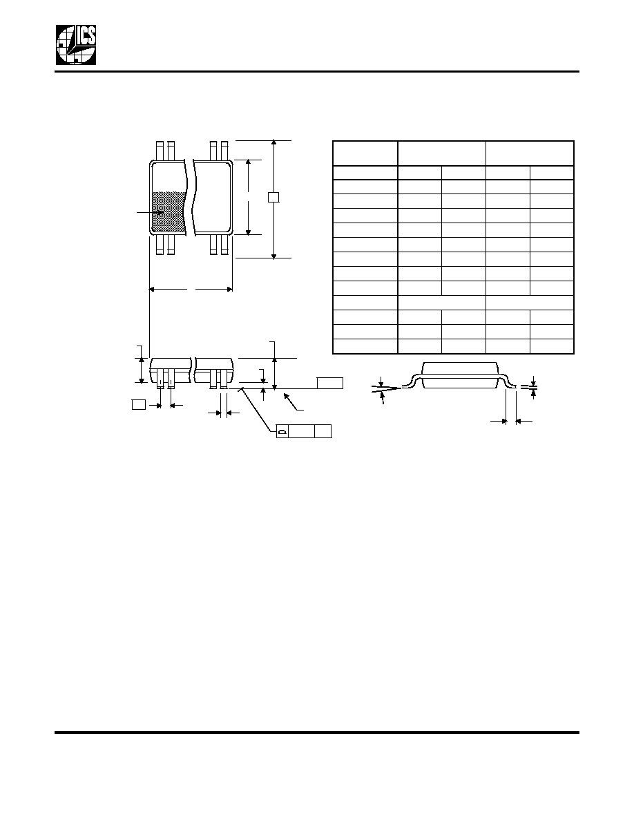
Package Outline and Package Dimensions
(28-pin SSOP, 150 mil Body)
Package dimensions are kept current with JEDEC Publication No. 95, MO-153
INDEX
AREA
1 2
28
D
E1
E
SEATING
PLANE
A
1
A
A
2
e
- C -
b
aaa
C
c
L
Millimeters
Inches
Symbol
Min
Max
Min
Max
A
1.35
1.75
.053
.069
A1
0.10
0.25
.0040
.010
A2
--
1.50
--
.059
b
0.20
0.30
.008
.012
C
0.18
0.25
.007
.010
D
9.80
10.00
.386
.394
E
5.80
6.20
.228
.244
E1
3.80
4.00
.150
.157
e
0.635 Basic
0.025 Basic
L
0.40
1.27
.016
.050
0
į
8
į
0
į
8
į
aaa
--
0.10
--
0.004
LVCMOS User Configurable Clock
MDS 525-07/08 A
9
Revision 101105
Integrated Circuit Systems, Inc.
525 Race Street, San Jose, CA 95126
tel (408) 297-1201
www.icst.com
ICS525-07/08
PRELIMINARY INFORMATION
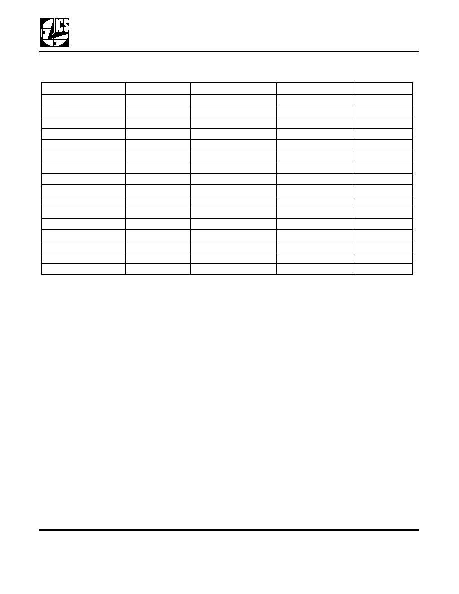
Ordering Information
Parts that are ordered with a "LF" suffix to the part number are the Pb-Free configuration and are RoHS compliant.
While the information presented herein has been checked for both accuracy and reliability, Integrated Circuit Systems (ICS)
assumes no responsibility for either its use or for the infringement of any patents or other rights of third parties, which would
result from its use. No other circuits, patents, or licenses are implied. This product is intended for use in normal commercial
applications. Any other applications such as those requiring extended temperature range, high reliability, or other extraordinary
environmental requirements are not recommended without additional processing by ICS. ICS reserves the right to change any
circuitry or specifications without notice. ICS does not authorize or warrant any ICS product for use in life support devices or
critical medical instruments.
Part / Order Number
Marking
Shipping Packaging
Package
Temperature
ICS525R-07
ICS525R-07
Tubes
28-pin SSOP
0 to +70
įC
ICS525R-07T
ICS525R-07
Tape and Reel
28-pin SSOP
0 to +70
įC
ICS525R-07LF
ICS525R-07LF
Tubes
28-pin SSOP
0 to +70
įC
ICS525R-07LFT
ICS525R-07LF
Tape and Reel
28-pin SSOP
0 to +70
įC
ICS525RI-07
ICS525R-I07
Tubes
28-pin SSOP
-40 to +85
įC
ICS525RI-07T
ICS525RI-07
Tape and Reel
28-pin SSOP
-40 to +85
įC
ICS525RI-07LF
ICS525RI07LF
Tubes
28-pin SSOP
-40 to +85
įC
ICS525RI-07LFT
ICS525RI07LF
Tape and Reel
28-pin SSOP
-40 to +85
įC
ICS525R-08
ICS525R-08
Tubes
28-pin SSOP
0 to +70
įC
ICS525R-08T
ICS525R-08
Tape and Reel
28-pin SSOP
0 to +70
įC
ICS525R-08LF
ICS525R-08LF
Tubes
28-pin SSOP
0 to +70
įC
ICS525R-08LFT
ICS525R-08LF
Tape and Reel
28-pin SSOP
0 to +70
įC
ICS525RI-08
ICS525RI-08
Tubes
28-pin SSOP
-40 to +85
įC
ICS525RI-08T
ICS525RI-08
Tape and Reel
28-pin SSOP
-40 to +85
įC
ICS525RI-08LF
ICS525RI08LF
Tubes
28-pin SSOP
-40 to +85
įC
ICS525RI-08LFT
ICS525RI08LF
Tape and Reel
28-pin SSOP
-40 to +85
įC