
ICS527-03
MDS 527-03 B
1
Revision 122804
Integrated Circuit Systems, Inc.
525 Race Street, San Jose, CA 95126
tel (408) 297-1201
www.icst.com
Clock Slicer User Configurable PECL Output Zero Delay Buffer
P r e l i m i n a r y I n f o r m a t i o n
Description
The ICS527-03 is the most flexible way to generate an
output clock from an input clock with zero skew. The
user can easily configure the device to produce nearly
any output clock that is multiplied or divided from the
input clock. The part supports non-integer
multiplications and divisions. Using Phase-Locked
Loop (PLL) techniques, the device accepts an input
clock up to 200 MHz and produces an output clock up
to 160 MHz.
The ICS527-03 aligns rising edges on CLKIN with
FBPECL at a ratio determined by the reference and
feedback dividers.
For a PECL input and output clock with zero delay, use
the ICS527-04.
Features
∑
Packaged as 28 pin SSOP (150 mil body)
∑
Synchronizes fractional clocks rising edges
∑
CMOS in to PECL out
∑
Pin selectable dividers
∑
Zero input to output skew
∑
User determines the output frequency - no software
needed
∑
Slices frequency or period
∑
Input clock frequency of 1.5 MHz to 200 MHz
∑
Output clock frequencies from 2.5 MHz to 160 MHz
∑
Very low jitter
∑
Duty cycle of 45/55
∑
Operating voltage of 3.3 V
∑
Advanced, low power CMOS process
Block Diagram
PECL
VDD
GND
2
2
Reference
Divider
Phase Comparator,
Charge Pump, and
Loop Filter
VCO
Output
Divider
7
7
2
R6:R0
F6:F0
S1:S0
PDTS
Feedback
Divider
FBPECL
FBPECL
PECL
CLKIN
1
0
Divide
by 2
1
0
Divide
by 2
DIV2
68 ohm
180 ohm
68 ohm
180 ohm
VDD
VDD
Clock Slicer User Configurable PECL Output Zero Delay Buffer
MDS 527-03 B
2
Revision 122804
Integrated Circuit Systems, Inc.
525 Race Street, San Jose, CA 95126
tel (408) 297-1201
www.icst.com
P r e l i m i n a r y I n f o r m a t i o n
ICS527-03
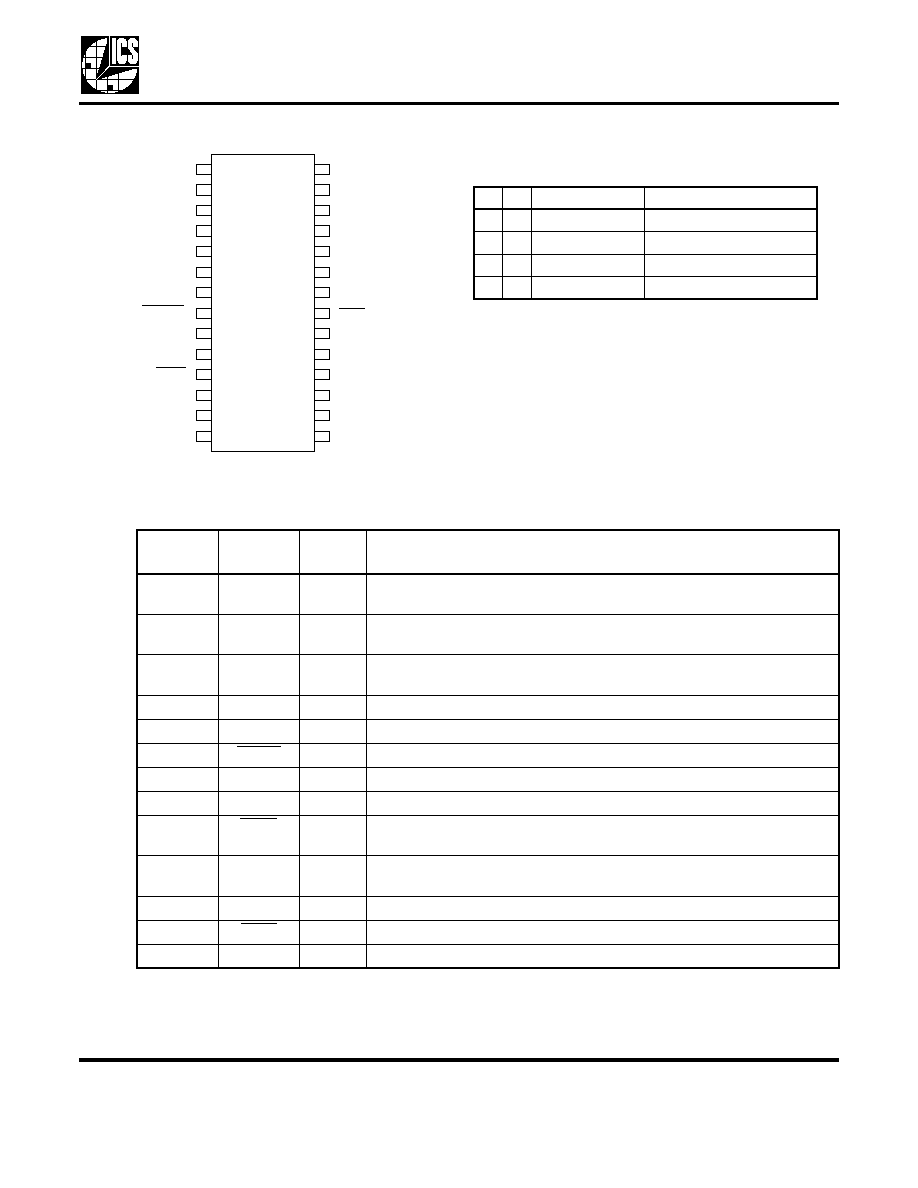
Pin Assignment
28 pin 150 mil body SSOP
Output Frequency and Output
Divider Table
Pin Descriptions
18
7
17
8
16
9
15
FBPECL
10
FBPECL
11
GND
12
PECL
13
CLKIN
14
PDTS
GND
F6
F0
F5
F3
F1
F4
22
21
20
19
F2
PECL
5
6
S1
VDD
VDD
24
23
R0
3
4
DIV2
S0
R1
26
25
R2
1
2
R5
R6
R3
28
27
R4
RES
S1 S0
Output Divider
Output Frequency (MHz)
0
0
2
10 - 80
0
1
4
5 - 40
1
0
8
2.5 - 20
1
1
1
20 -160
Pin
Number
Pin
Name
Pin
Type
Pin Description
1,2, 24-28
R5, R6,
R0-R4
Input
Reference divider word input pins determined by user. Forms a binary number
from 0 to 127. Internal pull-up.
3
DIV2
Input
Selects CLK2 function to output a SYNC signal or a divide by 2 of CLK1 based
on the table above. Internal pull-up.
4, 5
S0, S1
Input
Select pins for output divider determined by user. See table above. Internal
pull-up.
6, 23
VDD
Power
Connect to +3.3 V.
7
FPECL
Input
PECL feedback input.
8
FPECL
Input
Complementary PECL feedback input.
9, 20
GND
Power
Connect to ground
10
CLKIN
Input
Clock input.
11
PDTS
Input
Power Down. Active low. Turns off entire chip when low, both clock outputs are
tri-stated. Internal pull-up.
12-18
F0-F6
Input
Feedback divider word input pins determined by user. Forms a binary number
from 0 to 127. Internal pull-up
19
RES
BIAS
Resistor connection to VDD for setting level of PECL outputs.
21
PECL
Output
Complementary PECL input clock.
22
PECL
Output
PECL input clock.

Clock Slicer User Configurable PECL Output Zero Delay Buffer
MDS 527-03 B
3
Revision 122804
Integrated Circuit Systems, Inc.
525 Race Street, San Jose, CA 95126
tel (408) 297-1201
www.icst.com
P r e l i m i n a r y I n f o r m a t i o n
ICS527-03
External Components
Decoupling Capacitors
As with any high performance mixed-signal IC, the
ICS527-03 must be isolated from system power supply
noise to perform optimally.
Decoupling capacitors of 0.01µF must be connected
between each VDD and the PCB ground plane. They
must be connected close to the device to minimize lead
inductance.
Series Termination Resistor
Clock output traces over one inch should use series
termination. To series terminate a 50
trace (a
commonly used trace impedance), place a 33
resistor
in series with the clock line, as close to the clock output
pin as possible. The nominal impedance of the clock
output is 20
.
Determining (setting) the ICS527-03
Dividers
The user has full control in setting the desired output
clock over the range shown in the table on page 2. The
user should connect the divider select input pins
directly to ground (or VDD, although this is not required
because of internal pull-ups) during Printed Circuit
Board layout, so the ICS527-03 automatically produces
the correct clock when all components are soldered. It
is also possible to connect the inputs to parallel I/O
ports in order to switch frequencies.
The output of the ICS527-03 can be determined by the
following simple equation:
Where:
Reference Divider Word (RDW) = 0 to 127
Feedback Divider Word (FDW) = 0 to 127
FB Frequency is the same as either CLK1 or
CLK2 depending on feedback connection
Also, the following operating ranges should be
observed:
The output divide should be selected depending on
the frequency of CLK1. The table on page 2 gives
the ranges.
The dividers are expressed as integers. For example, if
a 50 MHz output on CLK1 is desired from a 40 MHz
input, the reference divider word (RDW) should be 2
and the feedback divider word (FDW) should be 3
which gives the required 5/4 multiplication. If multiple
choices of dividers are available, then the lowest
numbers should be used. In this example, the output
divide (OD) should be selected to be 2. Then R6:R0 is
0000010, F6:F0 is 0000011 and S1:S0 is 00. Also, this
example assumes CLK1 is connected to FBIN.
If you need assistance determining the optimum divider
settings, please send an e-mail to ics-mk@icst.com
with the desired input clock and the desired output
frequency.
FB Frequency
Input Frequency
FDW
2
+
RDW
2
+
------------------------
◊
=
300kHz
Input Frequency
RDW
2
+
-------------------------------------------
20 MHz
<
<
Clock Slicer User Configurable PECL Output Zero Delay Buffer
MDS 527-03 B
4
Revision 122804
Integrated Circuit Systems, Inc.
525 Race Street, San Jose, CA 95126
tel (408) 297-1201
www.icst.com
P r e l i m i n a r y I n f o r m a t i o n
ICS527-03
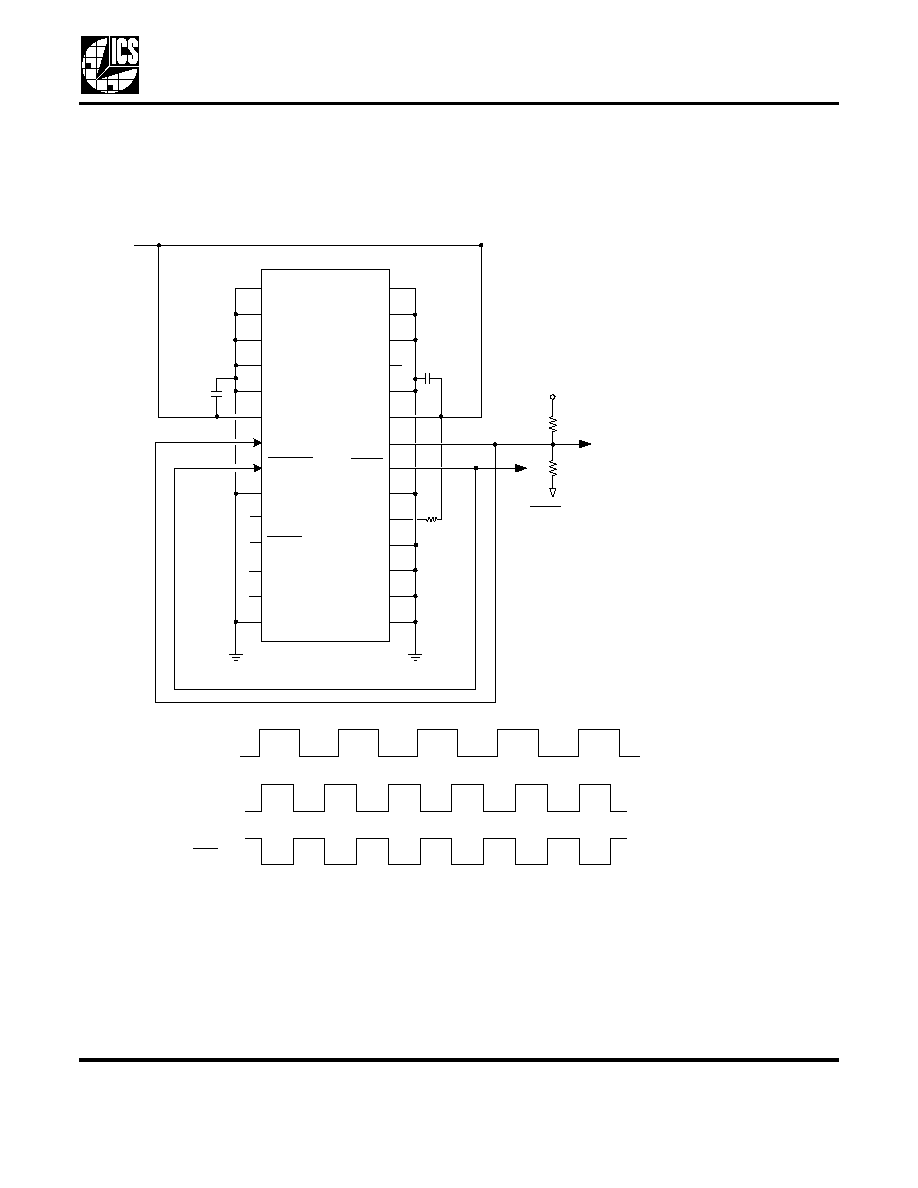
Typical Example
The following connection diagram shows the implementation of the example from the previous section.
This will generate a 50 MHz clock synchronously with a 40 MHz input. The layout diagram below will
produce the waveforms shown on the right.
Note: The series termination resistor is located before
the feedback
F6
FBPECL
F5
F4
GND
F3
CLKIN
PDTS
F0
F1
F2
PECL
PECL
GND
S1
VDD
R0
VDD
DIV2
S0
R2
R1
R5
R6
R4
R3
FBPECL
RES
0.01
F
0.01
F
VDD
560
50 MHz
PECL output resistor network is not shown, but
is identical to PECL
VDD
40 MHz
(PECLIN shown)
50 MHz PECL
50 MHz PECL

Clock Slicer User Configurable PECL Output Zero Delay Buffer
MDS 527-03 B
5
Revision 122804
Integrated Circuit Systems, Inc.
525 Race Street, San Jose, CA 95126
tel (408) 297-1201
www.icst.com
P r e l i m i n a r y I n f o r m a t i o n
ICS527-03
Multiple Output Example
In this example, an output clock of 125 MHz is used. Four copies of 50 MHz are required, de-skewed and
aligned to the 125 MHz input clock. The following solution uses the ICS554-01A which has buffers with low
pin to pin skew. The layout diagram below will produce the waveforms shown on the bottom.
PCB Layout Recommendations
For optimum device performance and lowest output
phase noise, the following guidelines should be
observed.
1) Each 0.01µF decoupling capacitor should be
mounted on the component side of the board as close
to the VDD pin as possible. No via's should be used
between decoupling capacitor and VDD pin. The PCB
trace to VDD pin should be kept as short as possible,
as should the PCB trace to the ground via.
2) PECL termination networks should be located as
close to the outputs as possible.
3) An optimum layout is one with all components on the
same side of the board, minimizing vias through other
signal layers. Other signal traces should be routed
away from the ICS527-03. This includes signal traces
just underneath the device, or on layers adjacent to the
ground plane layer used by the device.
Clock Slicer User Configurable PECL Output Zero Delay Buffer
MDS 527-03 B
6
Revision 122804
Integrated Circuit Systems, Inc.
525 Race Street, San Jose, CA 95126
tel (408) 297-1201
www.icst.com
P r e l i m i n a r y I n f o r m a t i o n
ICS527-03
Absolute Maximum Ratings
Stresses above the ratings listed below can cause permanent damage to the ICS527-03. These ratings,
which are standard values for ICS commercially rated parts, are stress ratings only. Functional operation of
the device at these or any other conditions above those indicated in the operational sections of the
specifications is not implied. Exposure to absolute maximum rating conditions for extended periods can
affect product reliability. Electrical parameters are guaranteed only over the recommended operating
temperature range.
Recommended Operation Conditions
DC Electrical Characteristics
Unless stated otherwise, VDD = 3.3V ±5%, Ambient Temperature 0 to +70
∞C
Item
Rating
Supply Voltage, VDD
7V
All Inputs and Outputs
-0.5V to VDD+0.5V
Ambient Operating Temperature
0 to +70
∞C
Storage Temperature
-65 to +150
∞C
Junction Temperature
175
∞C
Soldering Temperature
260
∞C
Parameter
Min.
Typ.
Max.
Units
Ambient Operating Temperature, ICS527R-02
0
+70
∞C
Ambient Operating Temperature, ICS527R-02I
0
+70
∞C
Power Supply Voltage (measured in respect to GND)
+3.15
+3.3
+3.45
V
Parameter
Symbol
Conditions
Min.
Typ.
Max.
Units
Operating Voltage
VDD
3.15
3.3
3.45
V
Supply Current
IDD
15 MHz in, 60MHz out,
no load
15
mA
Supply Current, Power Down
IDDPD
PDTS=0
20
µA
Input High Voltage
V
IH
2
V
Input Low Voltage
V
IL
0.8
V
Input High Voltage, PECLIN
and FBIN
V
IH
VDD/2+1
V
Input Low Voltage, PECLIN
and FBIN
V
IL
VDD/2-1
V
Output High Voltage
V
OH
I
OH
= -12 mA
2.4
V
Output Low Voltage
V
OL
I
OL
= 12 mA
0.4
V
Clock Slicer User Configurable PECL Output Zero Delay Buffer
MDS 527-03 B
7
Revision 122804
Integrated Circuit Systems, Inc.
525 Race Street, San Jose, CA 95126
tel (408) 297-1201
www.icst.com
P r e l i m i n a r y I n f o r m a t i o n
ICS527-03
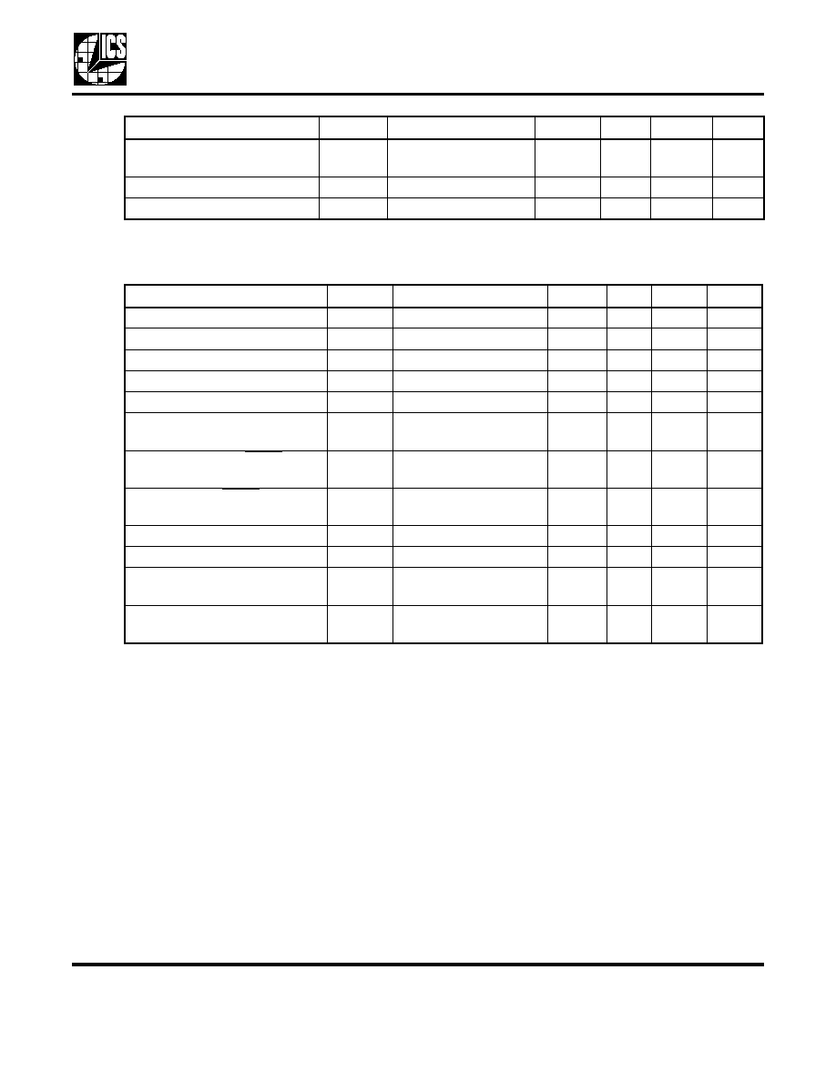
AC Electrical Characteristics
Unless stated otherwise, VDD = 3.3V ±5%, Ambient Temperature 0 to +70
∞C
Note 1: Assumes clocks with same rise time, measured from rising edges at VDD/2.
Input Capacitance, except
PECLIN and FBIN
C
IN
5
pF
Short Circuit Current
I
OS
±70
mA
On-chip pull-up resistor
R
PU
270
k
Parameter
Symbol
Conditions
Min.
Typ.
Max.
Units
Input Frequency
F
IN
1.5
200
MHz
Output Frequency, CLK1
F
OUT
0 to +70
∞C
2.5
160
MHz
-40 to +85
∞C
4
140
MHz
Output Rise Time
t
OR
0.8 to 2.0V, C
L
=15pF
1
ns
Output Fall Time
t
OF
2.0 to 0.8V, C
L
=15pF
1
ns
Output Duty Cycle (% high
time)
t
OD
Measured at VDD/2,
C
L
=15pF
45
50
55
%
Power Down Time, PDTS low to
clocks tri-stated
50
ns
Power Up ime, PDTS high to
clocks stable
10
ms
Absolute Clock Period Jitter
t
ja
Deviation from mean
± 90
ps
One sigma Clock Period Jitter
t
js
40
ps
Input to output skew
t
IO
PECLIN to CLK1,
Note 1
-250
250
ps
Device to device skew
t
pi
Common PECLIN,
measured at FBIN
0
500
ps
Parameter
Symbol
Conditions
Min.
Typ.
Max.
Units

Clock Slicer User Configurable PECL Output Zero Delay Buffer
MDS 527-03 B
8
Revision 122804
Integrated Circuit Systems, Inc.
525 Race Street, San Jose, CA 95126
tel (408) 297-1201
www.icst.com
P r e l i m i n a r y I n f o r m a t i o n
ICS527-03
Package Outline and Package Dimensions
(28 pin SSOP, 150 mil Body, 0.025 mm Pitch)
Package dimensions are kept current with JEDEC Publication No. 95, MO-153
Ordering Information
While the information presented herein has been checked for both accuracy and reliability, Integrated Circuit Systems (ICS)
assumes no responsibility for either its use or for the infringement of any patents or other rights of third parties, which would
result from its use. No other circuits, patents, or licenses are implied. This product is intended for use in normal commercial
applications. Any other applications such as those requiring extended temperature range, high reliability, or other extraordinary
environmental requirements are not recommended without additional processing by ICS. ICS reserves the right to change any
circuitry or specifications without notice. ICS does not authorize or warrant any ICS product for use in life support devices or
critical medical instruments
Part / Order Number
Marking
Shipping
packaging
Package
Temperature
ICS527R-03
ICS527R-03
Tubes
28 pin SSOP
0 to +70
∞C
ICS527R-03T
ICS527R-03
Tape and Reel
28 pin SSOP
0 to +70
∞C
INDEX
AREA
1 2
28
D
E1
E
SEATING
PLANE
A
1
A
A
2
e
- C -
b
aaa
C
c
L
Millimeters
Inches
Symbol
Min
Max
Min
Max
A
1.35
1.75
.053
.069
A1
0.10
0.25
.0040
.010
A2
--
1.50
--
.059
b
0.20
0.30
.008
.012
C
0.18
0.25
.007
.010
D
9.80
10.00
.386
.394
E
5.80
6.20
.228
.244
E1
3.80
4.00
.150
.157
e
0.635 Basic
0.025 Basic
L
0.40
1.27
.016
.050
0
∞
8
∞
0
∞
8
∞
aaa
--
0.10
--
0.004