ICS554-01
MDS 554-01 A
1
Revision 031901
I n t e g r a t e d C i r cu i t S y st e m s
G
5 2 5 Ra ce S t r e e t , S a n J o s e , C A 9 5 1 2 6
G
t e l ( 4 0 8 ) 2 9 5 - 9 8 0 0
G
w w w. i c s t . c o m
L
OW
S
KEW
1
TO
4 C
LOCK
B
UFFER
PECL I
N
, PECL O
UT
P R E L I M I N A R Y I N F O R M A T I O N
Description
The ICS554-01 is a low skew clock buffer with a single
complimentary PECL input to four PECL outputs. Part
of ICS' Clock Blocks
TM
family, this is our lowest skew
PECL clock buffer. For parts which do not require PECL
inputs or outputs, see the ICS553 for a 1 to 4 low skew
buffer, or the ICS552-02 for a 1 to 8 low skew buffer. For
more than 8 outputs see the MK74CBxxx Buffalo
TM
series of clock drivers.
ICS makes many non-PLL and PLL based low skew
output devices as well as Zero Delay Buffers to
synchronize clocks. Contact us for all of your clocking
needs.
Features
�
Outputs are skew matched to within 50ps
�
Packaged in 16 pin TSSOP
�
One PECL input to 4 PECL output clock drivers
�
Operating Voltages of 3.3V to 5V
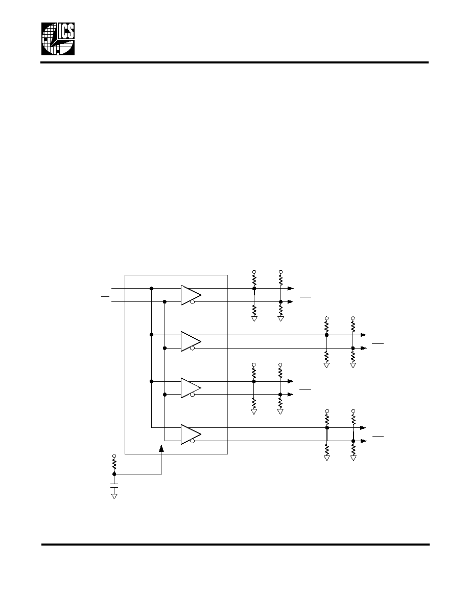
Block Diagram
IN
IN
RES
VDD
0.01mF
1.1k
Q0
Q0
VDD
62
62
270
270
Q1
Q1
VDD
62
62
270
270
Q2
Q2
VDD
62
62
270
270
Q3
Q3
VDD
62
62
270
270
L
OW
S
KEW
1
TO
4 C
LOCK
B
UFFER
PECL I
N
, PECL O
UT
MDS 554-01 A
2
Revision 031901
I n t e g r a t e d C i r c u i t S y s t e ms
G
5 2 5 R a c e S t r e e t , S a n J o s e , CA 9 5 1 2 6
G
t e l ( 4 0 8 ) 2 9 5 - 9 8 0 0
G
w w w. ic s t . c o m
P R E L I M I N A R Y I N F O R M A T I O N
ICS554-01
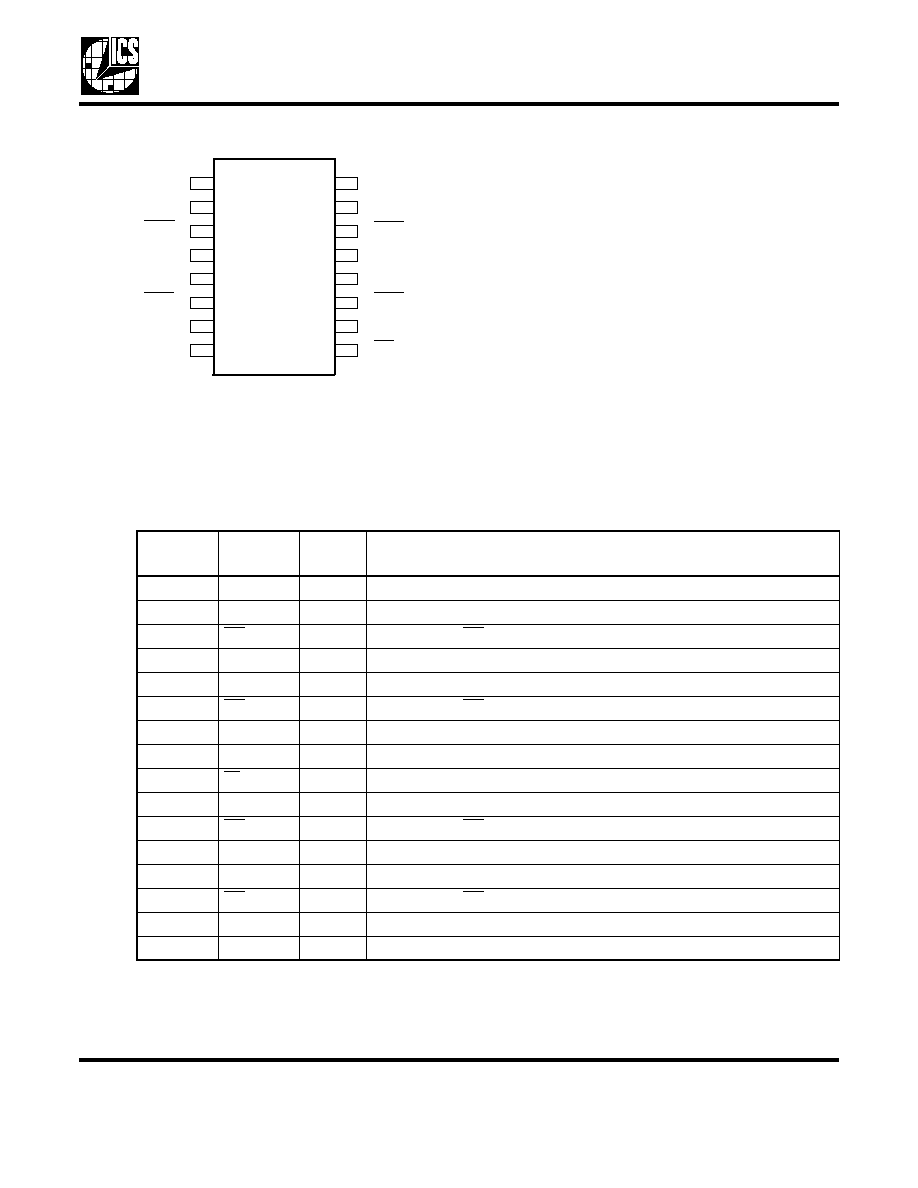
Pin Assignment
Pin Descriptions
1 2
1
1 1
2
1 0
3
9
N C
4
V D D
5
6
V D D
7
Q 0
8
Q 3
Q 3
Q 2
Q 1
IN
G N D
G N D
1 6
1 5
1 4
1 3
IN
R E S
1 6 P in T S S O P
Q 0
Q 1
Q 2
Pin
Number
Pin
Name
Pin
Type
Pin Description
1
NC
-
No Connect.
2
VDD
Power
Connect to +2.5 V, +3.3V or +5.0V. Must be the same as pin 15.
3
Q0
Output
Clock Output Q0
4
Q0
Output
Clock Output Q0
5
Q1
Output
Clock Output Q1
6
Q1
Output
Clock Output Q1
7
GND
Power
Ground
8
IN
Input
PECL Clock Input
9
IN
Input
Complementary PECL Clock Input
10
GND
Power
Ground
11
Q2
Output
Clock Output Q2
12
Q2
Output
Clock Output Q2
13
Q3
Output
Clock Output Q3
14
Q3
Output
Clock Output Q3
15
VDD
Power
Connect to +2.5V, +3.3V or +5.0V. Must be the same as pin 2
16
RES
Input
Bias Resistor Input.
L
OW
S
KEW
1
TO
4 C
LOCK
B
UFFER
PECL I
N
, PECL O
UT
MDS 554-01 A
3
Revision 031901
I n t e g r a t e d C i r c u i t S y s t e ms
G
5 2 5 R a c e S t r e e t , S a n J o s e , CA 9 5 1 2 6
G
t e l ( 4 0 8 ) 2 9 5 - 9 8 0 0
G
w w w. ic s t . c o m
P R E L I M I N A R Y I N F O R M A T I O N
ICS554-01
External Components
The ICS554-01 requires a decoupling capacitor of 0.01
�F to be connected between VDD on pin 2 and
GND on pin 7, as well as between VDD on pin 15 and GND on pin 10. These decoupling capacitors should
be placed as close to the device as possible. A 0.01
�F capacitor must be placed between the RES (pin 16)
and Ground, also, a resistor must be connected between the RES (pin 16) and VDD. Another eight
resistors are needed for the PECL outputs as shown on the block diagram on page 1. Suggested values of
these resistors are shown in the Block Diagram, but they can be varied to change the differential pair
output swing, and the DC level. Refer to Application Note, MAN09.
To achieve the low output skews that the ICS554-01 is capable of, careful attention must be paid to board
layout. Essentially, all 8 outputs must have identical terminations, identical loads, and identical trace
geometries. If they do not, the output skew will be degraded. For example, using a 30
series termination
on one output (with 33
on the others) will cause at least 15ps of skew.
Absolute Maximum Ratings
Stresses above the ratings listed below can cause permanent damage to the ICS554-01. These ratings,
which are standard values for ICS commercially rated parts, are stress ratings only. Functional operation of
the device at these or any other conditions above those indicated in the operational sections of the
specifications is not implied. Exposure to absolute maximum rating conditions for extended periods can
affect product reliability. Electrical parameters are guaranteed only over the recommended operating
temperature range.
Recommended Operation Conditions
Item
Rating
Supply Voltage, VDD
7V
All Inputs and Outputs
-0.5V to VDD+0.5V
Ambient Operating Temperature
0 to +70
�C
Storage Temperature
-65 to +150
�C
Junction Temperature
175
�C
Soldering Temperature
260
�C
Parameter
Min.
Typ.
Max.
Units
Ambient Operating Temperature
0
�
+70
�C
Power Supply Voltage (measured in respect to GND)
+3.15
+5.25
V

L
OW
S
KEW
1
TO
4 C
LOCK
B
UFFER
PECL I
N
, PECL O
UT
MDS 554-01 A
4
Revision 031901
I n t e g r a t e d C i r c u i t S y s t e ms
G
5 2 5 R a c e S t r e e t , S a n J o s e , CA 9 5 1 2 6
G
t e l ( 4 0 8 ) 2 9 5 - 9 8 0 0
G
w w w. ic s t . c o m
P R E L I M I N A R Y I N F O R M A T I O N
ICS554-01
DC Electrical Characteristics
VDD=3.3V �5%, Ambient temperature 0 to +70
�C, unless stated otherwise
Notes: 1. V
OH
and V
OL
can be set by the external resistor values on the PECL outputs.
2. IDD includes the current through the external resistors which can be modified.
AC Electrical Characteristics
VDD = 3.3V �5%
, Ambient Temperature 0 to +70
� C, unless stated otherwise
Parameter
Symbol
Conditions
Min.
Typ.
Max.
Units
Operating Voltage
VDD
3.15
5.25
V
Peak to Peak Input Voltage
IN
0.3
1.0
V
Input Common Mode Range
IN
VDD=3.3V
VDD-2.0
VDD-0.6
V
Input Common Mode Range
IN
VDD=5V
VDD-3.7
VDD-0.6
V
Input High Voltage, OE
V
IH
�
2
�
VDD
V
Input Low Voltage, OE
V
IL
�
�
�
0.4
V
Output High Voltage
V
OH
Note 1
VDD-1.2
V
Output Low Voltage
V
OL
Note 1
�
�
VDD-2.0
V
Operating Supply Current
IDD
No load, 135 MHz
67
mA
Short Circuit Current, 2.5V
I
OS
�40
mA
Short Circuit Current, 3.3V
I
OS
�50
mA
Short Circuit Current, 5V
I
OS
�60
mA
Parameter
Symbol
Conditions
Min.
Typ.
Max.
Units
Input Frequency
0
200
MHz
Propagation Delay (VDD=3.3V)
4
ns
Propagation Delay (VDD=5V)
3
ns
Output to output skew.
Crossing point of pair
0
50
ps

L
OW
S
KEW
1
TO
4 C
LOCK
B
UFFER
PECL I
N
, PECL O
UT
MDS 554-01 A
5
Revision 031901
I n t e g r a t e d C i r c u i t S y s t e ms
G
5 2 5 R a c e S t r e e t , S a n J o s e , CA 9 5 1 2 6
G
t e l ( 4 0 8 ) 2 9 5 - 9 8 0 0
G
w w w. ic s t . c o m
P R E L I M I N A R Y I N F O R M A T I O N
ICS554-01
Package Outline and Package Dimensions
(16 pin TSSOP, 173 Mil. Narrow Body)
Package dimensions are kept current with JEDEC Publication No. 95
Ordering Information
While the information presented herein has been checked for both accuracy and reliability, Integrated Circuit Systems (ICS)
assumes no responsibility for either its use or for the infringement of any patents or other rights of third parties, which would
result from its use. No other circuits, patents, or licenses are implied. This product is intended for use in normal commercial
applications. Any other applications such as those requiring extended temperature range, high reliability, or other extraordinary
environmental requirements are not recommended without additional processing by ICS. ICS reserves the right to change any
circuitry or specifications without notice. ICS does not authorize or warrant any ICS product for use in life support devices or
critical medical instruments.
Part / Order Number
Marking (both)
Shipping
packaging
Package
Temperature
ICS554G-01
ICS (top line)
Tubes
16 pin TSSOP
0 to +70
� C
ICS554G-01T
554G-01 (2nd line)
Tape and Reel
16 pin TSSOP
0 to +70
� C
D
E
H
c
b
e
a
A
L
Millimeters
Inches
Symbol
Min
Max
Min
Max
A
--
1.20
--
0.047
a
0.05
0.15
0.002
0.006
b
0.19
0.30
0.007
0.012
c
0.09
0.20
0.0035
0.008
D
4.90
5.10
0.193
0.201
E
4.30
4.50
0.169
0.177
e
0.65 Basic
0.0256 Basic
H
6.40 Basic
0.252 Basic
L
0.45
0.75
0.018
0.030