MDS 556-03 B
1
Revision 030204
I n t e gra t e d C i r c u i t S y s t e m s
5 2 5 R a c e S t r e e t , S a n J o s e, C A 9 5 1 2 6
t e l ( 4 0 8 ) 2 9 7 - 1 2 0 1
w w w. i c s t . c o m
Q
UAD
LVDS O
SCILLATOR
/B
UFFER
ICS556-03
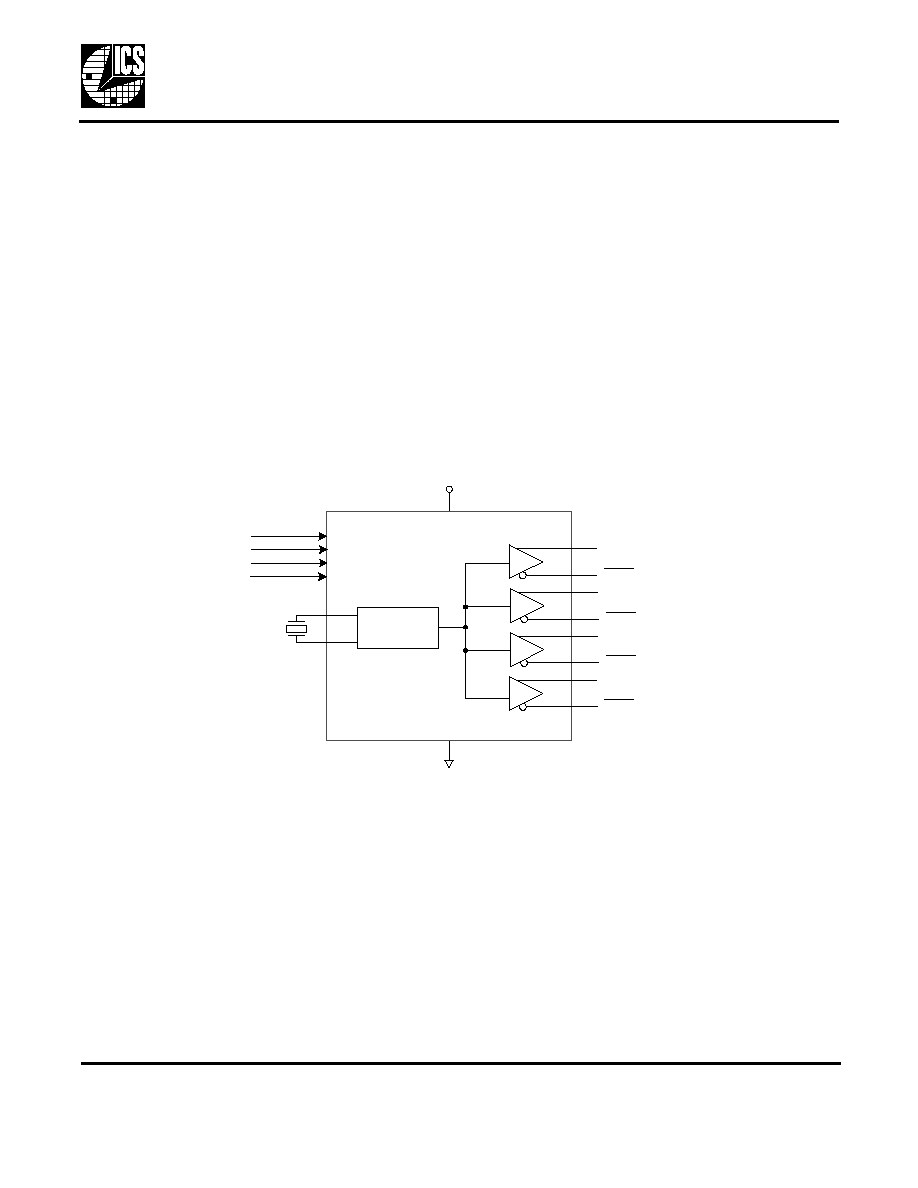
Description
The ICS556-03 is a clock oscillator with quad LVDS
outputs. Using a standard 25 MHz crystal, no additional
external components are required to generate quad
LVDS outputs at 25 MHz.
This product is intended for clock generation. It has low
output jitter (variation in the output period), but input to
output skew and jitter are not defined nor guaranteed.
Features
∑
Packaged in 16-pin TSSOP
∑
Requires no external components
∑
Low Phase Jitter: <1ps from 10 kHz to 10 MHz
∑
Quad, Differential LVDS outputs
∑
Operating voltage of 2.5 Volt
∑
Advanced, low-power, sub-micron CMOS process
Block Diagram
25MHz
Crystal
Oscillator
VDD
GND
CLKA
CLKA
LVDS
CLKB
CLKB
CLKC
CLKC
CLKD
CLKD
EN1
EN2
EN3
EN4
MDS 556-03 B
2
Revision 030204
I n t e gr a t e d C i r c u i t S y s t e m s
5 2 5 R a c e S t r e e t , S a n J o s e, C A 9 5 1 2 6
t e l ( 4 0 8 ) 2 9 7 - 1 2 0 1
w w w. i c s t . c o m
Quad LVDS Oscillator/Buffer
ICS556-03
Pin Assignment
Pin Descriptions
12
1
11
2
10
3
9
4
5
6
7
8
16
15
14
13
16-Pin (150 mil) SOIC
EN1
VDD
A
A
B
B
EN2
X2
EN4
EN3
D
D
C
C
GND
X1
Pin
Number
Pin
Name
Pin
Type
Pin Description
1
EN1
Input
Enable pin for Outputs A and A. EN1 high enables A, A outputs.
EN1 low tri states A, A outputs. No Pull-Up resistor.
2
VDD
Power
Power supply. Connect to 2.5 V.
3
A
Output
Differential clock output.
4
A
Output
Inverting differential clock output.
5
B
Output
Inverting differential clock output.
6
B
Output
Differential clock output.
7
EN2
Input
Enable pin for Outputs B and B. EN2 high enables B, B outputs.
EN2 low tri states B, B outputs. No Pull-Up resistor.
8
X2
Input
Crystal connection.
9
X1
Input
Crystal input.
10
GND
Power
Connect to ground.
11
C
Output
Differential clock output.
12
C
Output
Inverting differential clock output.
13
D
Output
Inverting differential clock output.
MDS 556-03 B
3
Revision 030204
I n t e gr a t e d C i r c u i t S y s t e m s
5 2 5 R a c e S t r e e t , S a n J o s e, C A 9 5 1 2 6
t e l ( 4 0 8 ) 2 9 7 - 1 2 0 1
w w w. i c s t . c o m
Quad LVDS Oscillator/Buffer
ICS556-03
External Component Selection
The ICS556-03 requires a minimum number of external
components for proper operation.
Decoupling Capacitors
A decoupling capacitor of 0.01
µF should be connected
between VDD and GND on pins 2 and 10 as close to
the ICS556-03 possible. For optimum device
performance, the decoupling capacitor should be
mounted on the component side of the PCB. Avoid the
use of vias in the decoupling circuit.
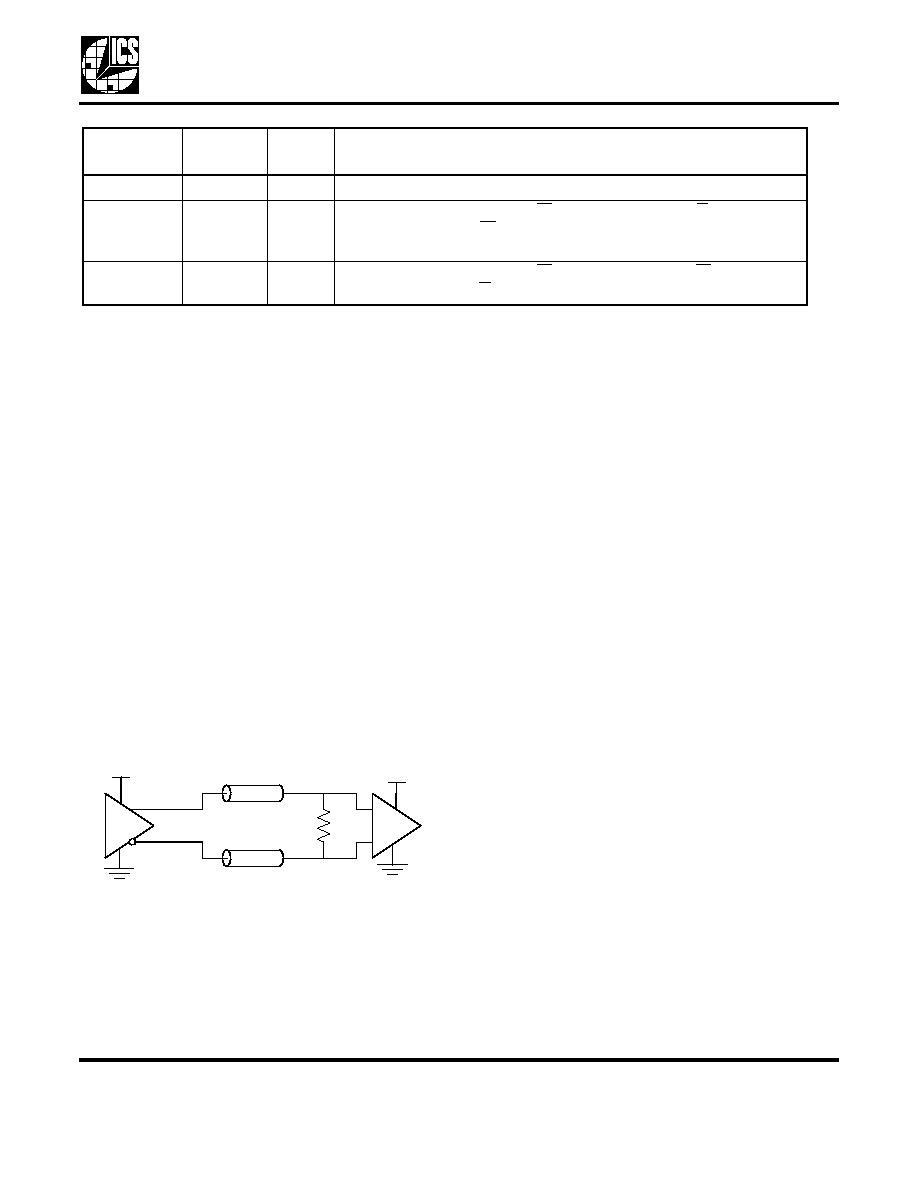
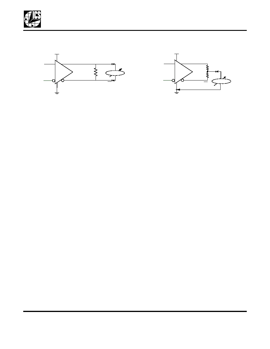
LVDS Driver Termination
A general LVDS interface is shown in Figure 2. In a 100
ohm differential transmission line environment, LVDS
drivers require a matched load termination of 100
across near the receiver input. For a multiple LVDS
outputs buffer, if only partial outputs are used, it is
recommended to terminate the un-used outputs.
Quartz Crystal
The ICS556-03, a quad 25 MHz LVDS Clock utilizes an
external crystal to generate 4 pairs of low phase noise
outputs. The crystal should be a fundamental mode,
parallel resonant. Crystal capacitors should be
connected from pins X1 to ground and X2 to ground to
optimize the initial accuracy. The value of these
capacitors is given by the following equation
Crystal Caps (pf)= (C
L
-12)x2
In the equation, CL is the crystal Load capacitance. So
for the crystal with 16pF load capacitance, two 8
pF[(16-12)x2] capacitors should be used.
The external crystal must be connected as close to the
chip as possible and should be on the same side of the
PCB as the ICS556-03. There should be no via's
between the crystal pins and the X1 and X2 device
pins. There should be no signal traces underneath or
close to the crystal.
14
D
Output
Differential clock output.
15
EN3
Input
Enable pin for Outputs C and C. EN4 high enables C, C outputs.
EN3 low tri states C, C outputs.No Pull-Up resistor.
16
EN4
Input
Enable pin for Outputs D and D. EN4 high enables D, D outputs.
EN4 low tri states D, D outputs.No Pull-Up resistor.
Pin
Number
Pin
Name
Pin
Type
Pin Description
R1
100 ohm
+
-
2.5V
2.5V
100 Ohm Differential Transmission Line
LVDS_Driver
Figure 2. Typical LVDS Driver
Termination

MDS 556-03 B
4
Revision 030204
I n t e gr a t e d C i r c u i t S y s t e m s
5 2 5 R a c e S t r e e t , S a n J o s e, C A 9 5 1 2 6
t e l ( 4 0 8 ) 2 9 7 - 1 2 0 1
w w w. i c s t . c o m
Quad LVDS Oscillator/Buffer
ICS556-03
Absolute Maximum Ratings
Stresses above the ratings listed below can cause permanent damage to the ICS556-03. These ratings,
which are standard values for ICS commercially rated parts, are stress ratings only. Functional operation of
the device at these or any other conditions above those indicated in the operational sections of the
specifications is not implied. Exposure to absolute maximum rating conditions for extended periods can
affect product reliability. Electrical parameters are guaranteed only over the recommended operating
temperature range.
Recommended Operation Conditions
Item
Rating
Supply Voltage, VDD
7 V
All Inputs and Outputs
-0.5 V to VDD+0.5 V
Ambient Operating Temperature
0 to +70
∞C
Storage Temperature
-65 to +150
∞C
Soldering Temperature
260
∞C
Parameter
Min.
Typ.
Max.
Units
Ambient Operating Temperature
0
+70
∞C
Power Supply Voltage (measured in respect to GND)
+2.375
+2.625
V
Reference crystal parameters
Refer to page 3

MDS 556-03 B
5
Revision 030204
I n t e gr a t e d C i r c u i t S y s t e m s
5 2 5 R a c e S t r e e t , S a n J o s e, C A 9 5 1 2 6
t e l ( 4 0 8 ) 2 9 7 - 1 2 0 1
w w w. i c s t . c o m
Quad LVDS Oscillator/Buffer
ICS556-03
DC Electrical Characteristics
VDD=2.5 V ±5%
, Ambient temperature 0 to +70
∞C, unless stated otherwise
Note 1: Outputs terminated with 50
to VDD/2
AC Electrical Characteristics
VDD = 2.5 V ±5%, Ambient Temperature 0 to +70
∞ C, CL=5 pF, unless stated otherwise
Parameter
Symbol
Conditions
Min.
Typ.
Max.
Units
Operating Voltage
VDD
2.375
2.625
V
Output High Voltage
V
OH
Note 1
1.375
V
Output Low Voltage
V
OL
Note 1
1.125
V
Input High Voltage (EN1,
EN2,EN3 & EN4)
V
IH
2.0
V
Input High Voltage (EN1,
EN2,EN3 & EN4)
V
IL
0.5
V
Operating Supply Current
IDD
OE1:4:1
17
mA
OE1:4:0
4
mA
Short Circuit Current
I
OS
±50
mA
Parameter
Conditions
Min.
Typ.
Max. Units
Input Frequency
25
MHz
Output Frequency
25
MHz
Differential Output Voltages (V
OD
)
250
350
450
mV
V
OD
V
OD
Magnitude Change
-40
0
40
mV
Offset Voltage (V
OS
)
1.125
1.25
1.375
V
V
OS
V
OS
Magnitude Change
3
25
mV
Differential Output Short Circuit Current (I
OSD
)
-3.5
mA
Output Short Circuit Current (I
OS
)
-3.5
mA
Output Rise Time
20% to 80%, no load
0.8
1.2
ns
Output Fall Time
20% to 80%, no load
0.8
1.2
ns
Output Clock Duty Cycle
Measured at 1.25V,
45
50
55
%
Output Short Circuit Current
±50
mA
Channel Output to output Skew
20
100
ps
Part to Part Skew
1.5
ns
Maximum Output Jitter (p-p)
40
ps
Phase Jitter (RMS)
Phase Noise integrated
from 10 kHz to 10 MHz
2
1.0
ps
MDS 556-03 B
6
Revision 030204
I n t e gr a t e d C i r c u i t S y s t e m s
5 2 5 R a c e S t r e e t , S a n J o s e, C A 9 5 1 2 6
t e l ( 4 0 8 ) 2 9 7 - 1 2 0 1
w w w. i c s t . c o m
Quad LVDS Oscillator/Buffer
ICS556-03
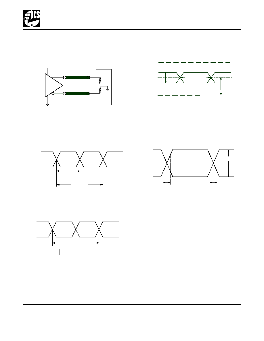
Parameter Measurement Information
2.5V O
UTPUT
L
OAD
AC T
EST
C
IRCUIT
LVDS
V
DD
= 2.5V±5%
SCOPE
50
50
Z = 50
Z = 50
Qx
nQx
tPW & tPERIOD
nCLK
CLK
t
PERIOD
Pulse Width
P
HASE
J
ITTER
nCLK
CLK
t(
)
V
OH
V
OL
t
jit(
) =
t
(
) -
t
(
)
mean
= Phase Jitter
D
IFFERENTIAL
I
NPUT
L
EVEL
VOS
Cross Points
VDD
VOD
nCLK
CLK
GND
Clock
Outputs
80%
80%
20%
20%
t
OR
t
OF
O
UTPUT
R
ISE
/F
ALL
T
IME
V
OD
MDS 556-03 B
7
Revision 030204
I n t e gr a t e d C i r c u i t S y s t e m s
5 2 5 R a c e S t r e e t , S a n J o s e, C A 9 5 1 2 6
t e l ( 4 0 8 ) 2 9 7 - 1 2 0 1
w w w. i c s t . c o m
Quad LVDS Oscillator/Buffer
ICS556-03
V
OD
S
ETUP
LVDS
V
DD
100
out
out
DC Input
V
OD
/
V
OD
V
OS
S
ETUP
LVDS
V
DD
50
out
DC Input
V
OS
/
V
OS
out
50
MDS 556-03 B
8
Revision 030204
I n t e gr a t e d C i r c u i t S y s t e m s
5 2 5 R a c e S t r e e t , S a n J o s e, C A 9 5 1 2 6
t e l ( 4 0 8 ) 2 9 7 - 1 2 0 1
w w w. i c s t . c o m
Quad LVDS Oscillator/Buffer
ICS556-03
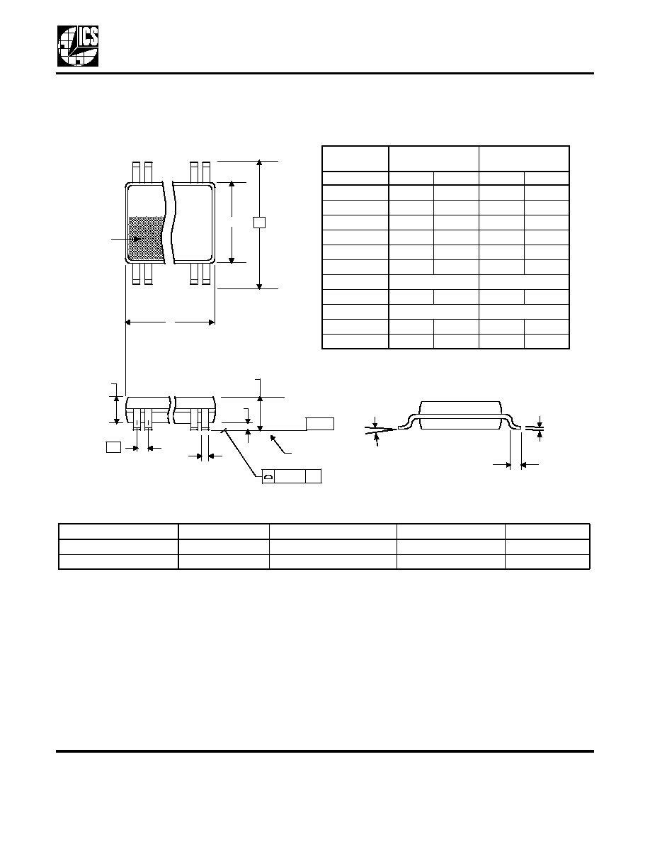
Package Outline and Package Dimensions
(16-pin TSSOP, 4.40 mm Body, 0.65 mm Pitch)
Package dimensions are kept current with JEDEC Publication No. 95
Ordering Information
While the information presented herein has been checked for both accuracy and reliability, Integrated Circuit Systems (ICS)
assumes no responsibility for either its use or for the infringement of any patents or other rights of third parties, which would
result from its use. No other circuits, patents, or licenses are implied. This product is intended for use in normal commercial
applications. Any other applications such as those requiring extended temperature range, high reliability, or other extraordinary
environmental requirements are not recommended without additional processing by ICS. ICS reserves the right to change any
circuitry or specifications without notice. ICS does not authorize or warrant any ICS product for use in life support devices or
critical medical instruments.
Part / Order Number
Marking
Shipping/Packaging
Package
Temperature
ICS556G-03I
ICS556-03I
Tubes
16-pin TSSOP
-40∞ to +85∞C
ICS556G-03IT
ICS556-03I
Tape and Reel
16-pin TSSOP
-40∞ to +85∞C
INDEX
AREA
1 2
16
D
E1
E
SEATING
PLANE
A
1
A
A
2
e
- C -
b
.10 (.004)
C
c
L
Millimeters
Inches
Symbol
Min
Max
Min
Max
A
--
1.20
--
0.047
A1
0.05
0.15
0.002
0.006
A2
0.80
1.05
0.032
0.041
b
0.19
0.30
0.007
0.012
C
0.09
0.20
0.0035
0.008
D
4.90
5.1
0.193
0.201
E
6.40 BASIC
0.252 BASIC
E1
4.30
4.50
0.169
0.177
e
0.65 Basic
0.0256 Basic
L
0.45
0.75
0.018
0.030
0
∞
8
∞
0
∞
8
∞