ICS556-04
MDS 556-04 C
1
Revision 030905
I n t e gra t e d C i r c u i t S y s t e m s
5 2 5 R a c e S t r e e t , S a n J o s e, C A 9 5 1 2 6
t e l ( 4 0 8 ) 2 9 7 - 1 2 0 1
w w w. i c s t . c o m
L
OW
S
KEW
1
TO
4 C
LOCK
B
UFFER
Description
The ICS556-04 is a low-skew, crystal input compatible
clock buffer with oscillator. This device offers the lowest
skew.
See the ICS552-02 for a 1-to-8 low skew buffer. For
more than eight outputs see the MK74CBxxx Buffalo
TM
series of clock drivers.
ICS makes many non-PLL and PLL-based low-skew
output devices. Contact ICS for all of your clocking
needs.
Features
∑
Extremely low-skew outputs (50 ps maximum)
∑
Packaged in 8-pin SOIC
∑
Operating voltages of 2.5 to 5.0 V
∑
Low-power CMOS technology
∑
Industrial temperature range
∑
Available in Pb (lead) free package
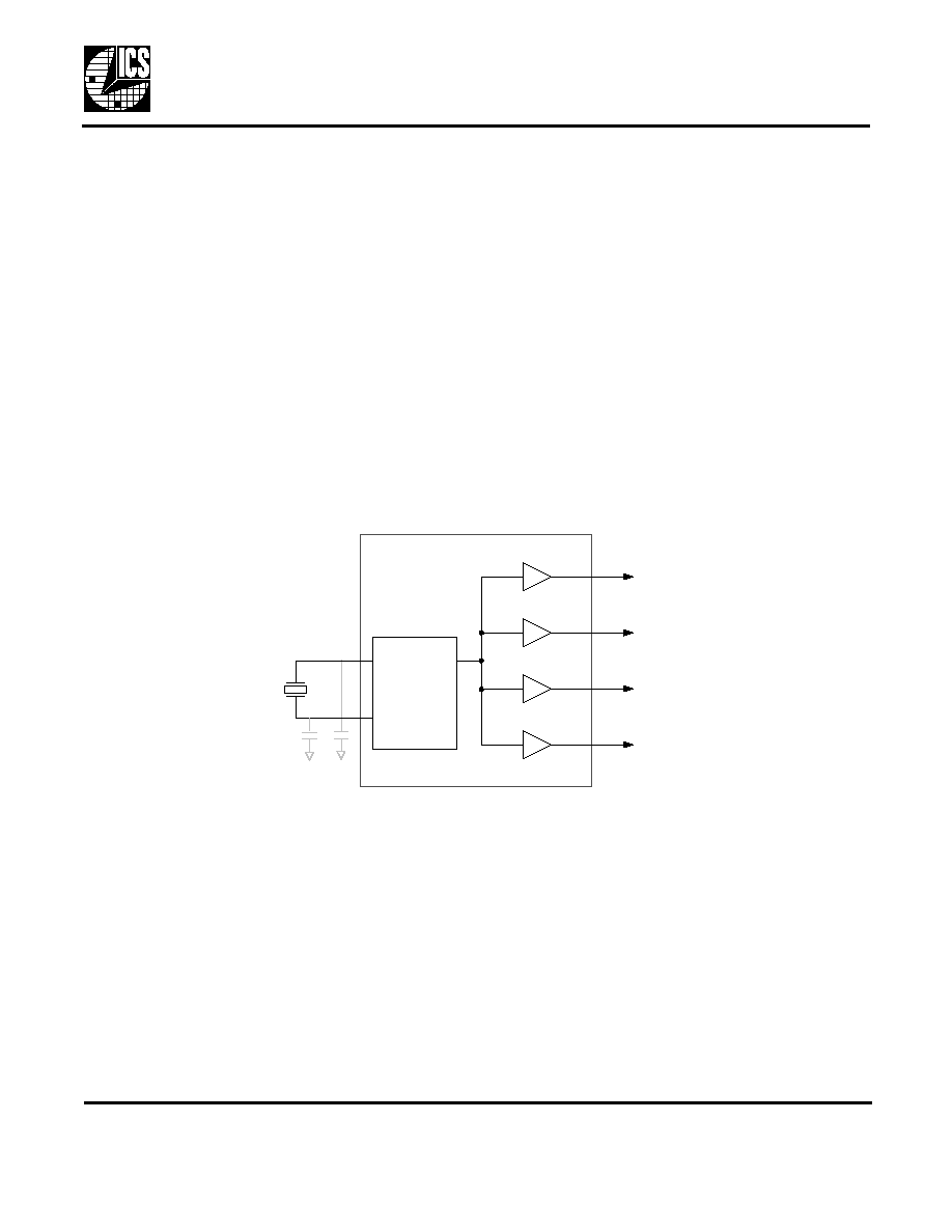
Block Diagram
Q0
Q1
Q2
Q3
X1/ICLK
X2
5 to 27 MHz
Crystal or clock
Crystal
Oscillator/
Buffer
Optional crystal
capacitors
L
OW
S
KEW
1
TO
4 C
LOCK
B
UFFER
MDS 556-04 C
2
Revision 030905
I n t e gr a t e d C i r c u i t S y s t e m s
5 2 5 R a c e S t r e e t , S a n J o s e, C A 9 5 1 2 6
t e l ( 4 0 8 ) 2 9 7 - 1 2 0 1
w w w. i c s t . c o m
ICS556-04
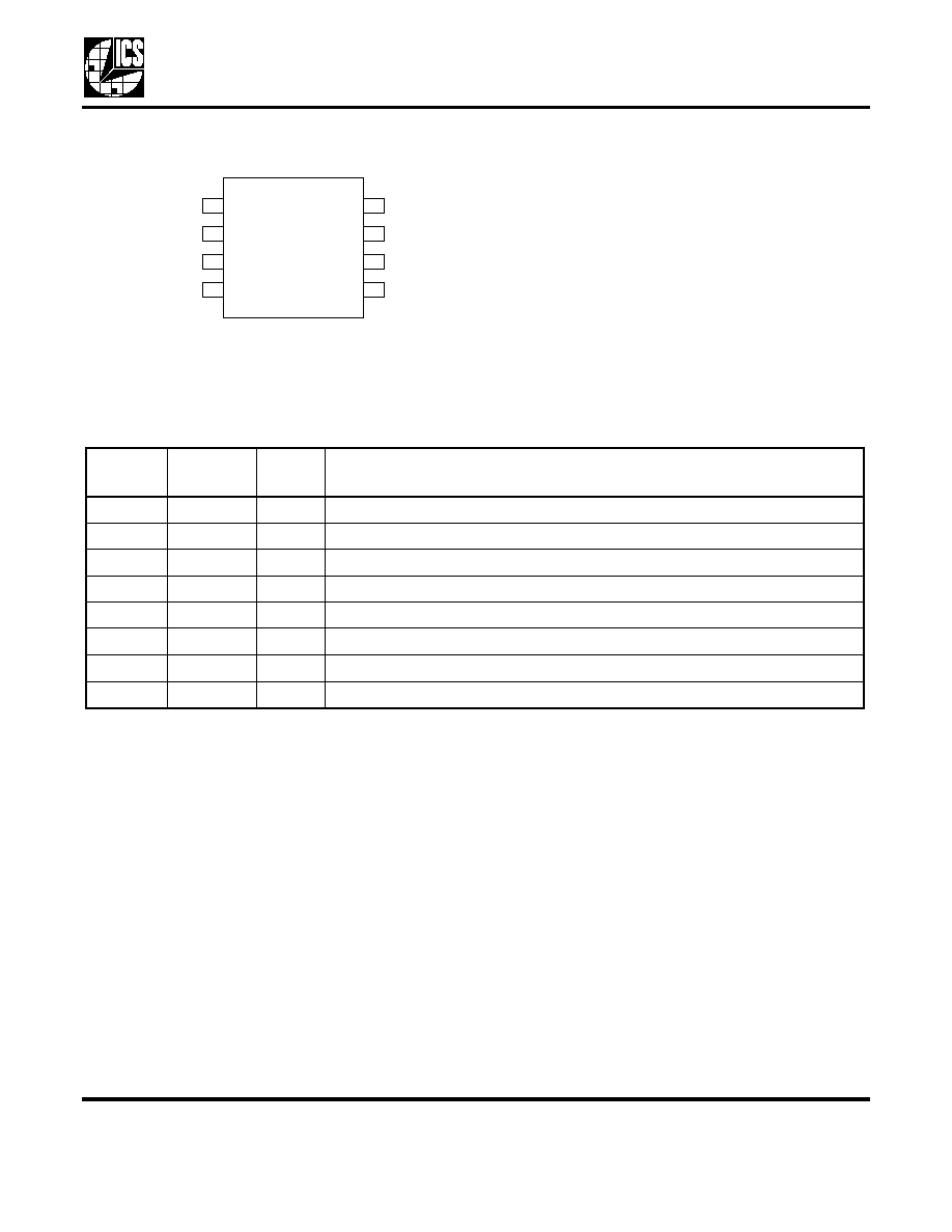
Pin Assignment
Pin Descriptions
External Components
A minimum number of external components are required for proper operation. A decoupling capacitor of 0.01
µF
should be connected between VDD on pin 1 and GND on pin 4, as close to the device as possible. A 33
series
terminating resistor may be used on each clock output if the trace is longer than 1 inch.
To achieve the low output skew that the ICS556-04 is capable of, careful attention must be paid to board layout.
Essentially, all four outputs must have identical terminations, identical loads, and identical trace geometries. If not,
the output skew will be degraded. For example, using a 30
series termination on one output (with 33 on the
others) will cause at least 15 ps of skew.
Crystal Information
The crystal used should be a fundamental mode (do not use third overtone), parallel resonant. Crystal capacitors
should be connected from pins X1 to ground and X2 to ground to optimize the initial accuracy. The value of these
capacitors is given by the following equation:
Crystal caps (pF) = (CL - 6) x 2
In the equation, CL is the crystal load capacitance. So, for a crystal with a 16 pF load capacitance, two 20 pF [(16-6)
x 2] capacitors should be used.
1
2
3
X 1 / I CL K
4
V DD
GND
Q4
Q3
8
7
6
5
X2
8 - p i n ( 1 5 0 mi l ) S OI C
Q1
Q2
Pin
Number
Pin
Name
Pin
Type
Pin Description
1
VDD
Power
Connect to +2.5 V, +3.3 V or +5.0 V.
2
X1/ICLK
Input
Crystal or clock input (5 V tolerant input). Connect to 5 to 27 MHz input.
3
X2
Input
Connect to a fundamental mode crystal. Leave open for clock input.
4
GND
Power
Connect to ground.
5
Q1
Output
Clock Output 1.
6
Q2
Output
Clock Output 2.
7
Q3
Output
Clock Output 3.
8
Q4
Output
Clock Output 3.

L
OW
S
KEW
1
TO
4 C
LOCK
B
UFFER
MDS 556-04 C
3
Revision 030905
I n t e gr a t e d C i r c u i t S y s t e m s
5 2 5 R a c e S t r e e t , S a n J o s e, C A 9 5 1 2 6
t e l ( 4 0 8 ) 2 9 7 - 1 2 0 1
w w w. i c s t . c o m
ICS556-04
Absolute Maximum Ratings
Stresses above the ratings listed below can cause permanent damage to the ICS556-04. These ratings,
which are standard values for ICS commercially rated parts, are stress ratings only. Functional operation of
the device at these or any other conditions above those indicated in the operational sections of the
specifications is not implied. Exposure to absolute maximum rating conditions for extended periods can
affect product reliability. Electrical parameters are guaranteed only over the recommended operating
temperature range.
Recommended Operation Conditions
DC Electrical Characteristics
VDD=2.5 V ±5%, Ambient temperature -40 to +85
∞C, unless stated otherwise
Item
Rating
Supply Voltage, VDD
7 V
Output Enable and All Outputs
-0.5 V to VDD+0.5 V
ICLK
-0.5 V to 5.5 V
Ambient Operating Temperature
-40 to +85
∞C
Storage Temperature
-65 to +150
∞C
Junction Temperature
125
∞C
Soldering Temperature
260
∞C
Parameter
Min.
Typ.
Max.
Units
Ambient Operating Temperature
-40
+85
∞C
Power Supply Voltage (measured in respect to GND)
+2.375
+5.25
V
Parameter
Symbol
Conditions
Min.
Typ.
Max.
Units
Operating Voltage
VDD
2.375
2.625
V
Input High Voltage
V
IH
2.0
V
Input Low Voltage
V
IL
0.8
V
Output High Voltage
V
OH
I
OH
= -12 mA
2
V
Output Low Voltage
V
OL
I
OL
= 12 mA
0.4
V
Operating Supply Current
IDD
No load, 27MHz
25
mA
Nominal Output Impedance
Z
O
20
Short Circuit Current
I
OS
±28
mA

L
OW
S
KEW
1
TO
4 C
LOCK
B
UFFER
MDS 556-04 C
4
Revision 030905
I n t e gr a t e d C i r c u i t S y s t e m s
5 2 5 R a c e S t r e e t , S a n J o s e, C A 9 5 1 2 6
t e l ( 4 0 8 ) 2 9 7 - 1 2 0 1
w w w. i c s t . c o m
ICS556-04
DC Electrical Characteristics (continued)
VDD=3.3 V ±5%
, Ambient temperature -40 to +85
∞C, unless stated otherwise
VDD=5 V ±5%
, Ambient temperature -40 to +85
∞C, unless stated otherwise
Notes:
1. Nominal switching threshold is VDD/2
Parameter
Symbol
Conditions
Min.
Typ.
Max.
Units
Operating Voltage
VDD
3.15
3.45
V
Input High Voltage
V
IH
2.0
V
Input Low Voltage
V
IL
0.8
V
Output High Voltage
V
OH
I
OH
= -25 mA
2.4
V
Output Low Voltage
V
OL
I
OL
= 25 mA
0.4
V
Output High Voltage (CMOS
Level)
V
OH
I
OH
= -12 mA
VDD-0.4
V
Operating Supply Current
IDD
No load, 27 MHz
35
mA
Nominal Output Impedance
Z
O
20
Short Circuit Current
I
OS
±50
mA
Parameter
Symbol
Conditions
Min.
Typ.
Max.
Units
Operating Voltage
VDD
4.75
5.25
V
Input High Voltage
V
IH
2.0
V
Input Low Voltage
V
IL
0.8
V
Output High Voltage
V
OH
I
OH
= -35 mA
2.4
V
Output Low Voltage
V
OL
I
OL
= 35 mA
0.4
V
Output High Voltage (CMOS
Level)
V
OH
I
OH
= -12 mA
VDD-0.4
V
Operating Supply Current
IDD
No load, 27 MHz
45
mA
Nominal Output Impedance
Z
O
20
Short Circuit Current
I
OS
±80
mA

L
OW
S
KEW
1
TO
4 C
LOCK
B
UFFER
MDS 556-04 C
5
Revision 030905
I n t e gr a t e d C i r c u i t S y s t e m s
5 2 5 R a c e S t r e e t , S a n J o s e, C A 9 5 1 2 6
t e l ( 4 0 8 ) 2 9 7 - 1 2 0 1
w w w. i c s t . c o m
ICS556-04
AC Electrical Characteristics
VDD = 2.5 V ±5%, Ambient Temperature -40 to +85
∞C, unless stated otherwise
VDD = 3.3 V ±5%, Ambient Temperature -40 to +85
∞C, unless stated otherwise
VDD = 5 V ±5%, Ambient Temperature -40 to +85
∞C, unless stated otherwise
Notes: 1. Between any two outputs with equal loading.
Thermal Characteristics
Parameter
Symbol
Conditions
Min.
Typ.
Max.
Units
Input Frequency
5
27
MHz
Output Rise Time
t
OR
0.8 to 2.0 V, C
L
=15 pF
1.8
2.5
ns
Output Fall Time
t
OF
2.0 to 0.8 V, C
L
=15 pF
1.8
2.5
ns
Output to output skew
Note 1
Rising edges at VDD/2
0
50
ps
Duty Cycle
Measured at VDD/2
45
50
55
%
Parameter
Symbol
Conditions
Min.
Typ.
Max.
Units
Input Frequency
5
27
MHz
Output Rise Time
t
OR
0.8 to 2.0 V, C
L
=15 pF
0.6
1.0
ns
Output Fall Time
t
OF
2.0 to 0.8 V, C
L
=15 pF
0.6
1.0
ns
Output to output skew
Note 1
Rising edges at VDD/2
0
50
ps
Duty Cycle
Measured at VDD/2
45
50
55
%
Phase Noise at 1MHz from
carrier
-125
dBc/Hz
Clock Jitter RMS 1KHz to 1MHz
6
ps
Parameter
Symbol
Conditions
Min.
Typ.
Max.
Units
Input Frequency
5
27
MHz
Output Rise Time
t
OR
0.8 to 2.0 V, C
L
=15 pF
0.3
0.7
ns
Output Fall Time
t
OF
2.0 to 0.8 V, C
L
=15 pF
0.3
0.7
ns
Output to output skew
Note 1
Rising edges at VDD/2
0
50
ps
Duty Cycle
Measured at VDD/2
45
50
55
%
Parameter
Symbol
Conditions
Min.
Typ.
Max.
Units
Thermal Resistance Junction to
Ambient
JA
Still air
150
∞C/W
JA
1 m/s air flow
140
∞C/W
JA
3 m/s air flow
120
∞C/W
Thermal Resistance Junction to Case
JC
40
∞C/W

L
OW
S
KEW
1
TO
4 C
LOCK
B
UFFER
MDS 556-04 C
6
Revision 030905
I n t e gr a t e d C i r c u i t S y s t e m s
5 2 5 R a c e S t r e e t , S a n J o s e, C A 9 5 1 2 6
t e l ( 4 0 8 ) 2 9 7 - 1 2 0 1
w w w. i c s t . c o m
ICS556-04
Package Outline and Package Dimensions
(8-pin SOIC, 150 Mil. Narrow Body)
Package dimensions are kept current with JEDEC Publication No. 95
Ordering Information
"LF" denotes Pb free package.
While the information presented herein has been checked for both accuracy and reliability, Integrated Circuit Systems (ICS)
result from its use. No other circuits, patents, or licenses are implied. This product is intended for use in normal commercial
applications. Any other applications such as those requiring extended temperature range, high reliability, or other extraordinary
environmental requirements are not recommended without additional processing by ICS. ICS reserves the right to change any
circuitry or specifications without notice. ICS does not authorize or warrant any ICS product for use in life support devices or
critical medical instruments.
Part / Order Number
Marking
Shipping Packaging
Package
Temperature
ICS556M-04I
556M-04I
Tubes
8-pin SOIC
-40 to +85
∞C
ICS556M-04IT
556M-04I
Tape and Reel
8-pin SOIC
-40 to +85
∞C
ICS556M-04ILF
556M04IL
Tubes
8-pin SOIC
-40 to +85
∞C
ICS556M-04ILFT
556M04IL
Tape and Reel
8-pin SOIC
-40 to +85
∞C
INDEX
AREA
1 2
8
D
E
SEATING
PLANE
A1
A
e
- C -
B
.10 (.004)
C
C
L
H
h x 45
Millimeters
Inches
Symbol
Min
Max
Min
Max
A
1.35
1.75
.0532
.0688
A1
0.10
0.25
.0040
.0098
B
0.33
0.51
.013
.020
C
0.19
0.25
.0075
.0098
D
4.80
5.00
.1890
.1968
E
3.80
4.00
.1497
.1574
e
1.27 BASIC
0.050 BASIC
H
5.80
6.20
.2284
.2440
h
0.25
0.50
.010
.020
L
0.40
1.27
.016
.050
0
∞
8
∞
0
∞
8
∞