
ICS557-08
MDS 557-08 C
1
Revision 021606
I n t e gra t e d C i r c u i t S y s t e m s
5 2 5 R a c e S t r e e t , S a n J o s e, C A 9 5 1 2 6
t e l ( 4 0 8 ) 2 9 7 - 1 2 0 1
w w w. i c s t . c o m
2:1 M
ULTIPLEXER
C
HIP
FOR
PCI-E
XPRESS
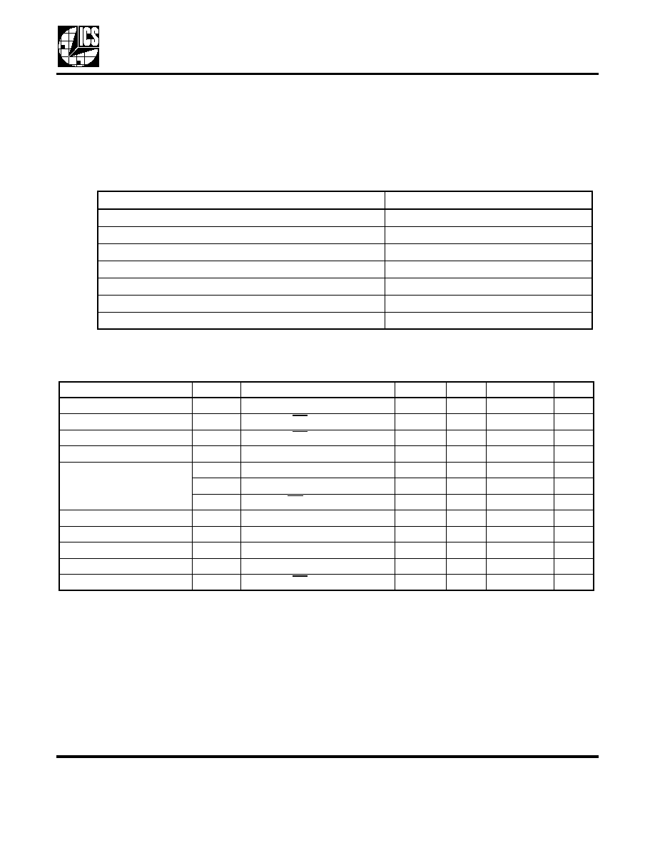
Description
The ICS557-08 is a 2:1 multiplexer chip that allows the
user to select one of the two HCSL (Host Clock Signal
Level) or LVDS input pairs and fan out to one pair of
differential HCSL or LVDS outputs. This chip is suited
especially for PCI-Express applications, where there is
a need to select the PCI-Express clock either locally
from the PCI-E card or from the motherboard.
Features
∑
Packaged in 16-pin TSSOP
∑
Available in Pb (lead) free package
∑
Operating voltage of 3.3 V
∑
Low power consumption
∑
Input clock frequency of up to 200 MHz for HCSL and
up to 100 MHz for LVDS
∑
Jitter 60 ps (cycle-to-cycle)
Block Diagram
VDD
Rr (IREF)
CLK
CLK
SEL
GND
IN1
IN1
IN2
IN2
MUX
2 to 1
OE
3
3
PD
MDS 557-08 C
2
Revision 021606
I n t e gr a t e d C i r c u i t S y s t e m s
5 2 5 R a c e S t r e e t , S a n J o s e, C A 9 5 1 2 6
t e l ( 4 0 8 ) 2 9 7 - 1 2 0 1
w w w. i c s t . c o m
ICS557-08
2:1 Multiplexer Chip for PCI-Express
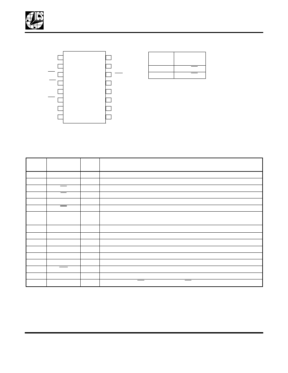
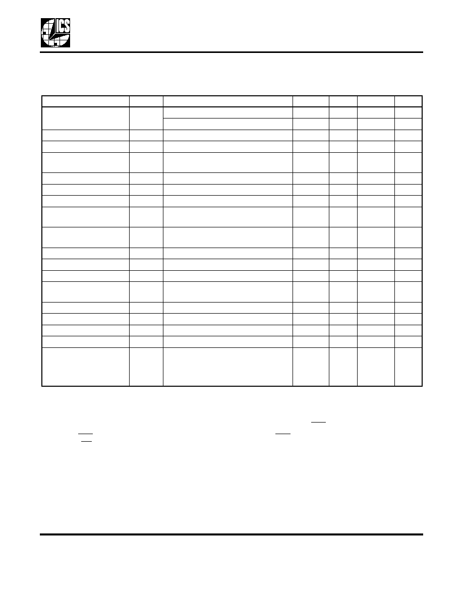
Pin Assignment
Select Table
Pin Descriptions
1
2
3
IN2
4
IN1
5
6
GND
7
8
GND
VDD
SEL
IN2
IN1
16
PD
GND
CLK
VDD
15
14
13
12
11
10
9
16-pin (173 mil) TSSOP
OE
VDD
IREF
CLK
SEL
Input Pair
selected
0
IN2/ IN2
1
IN1/ IN1
Pin
Pin
Name
Pin
Type
Pin Description
1
VDD
Power
Connect to +3.3 V. Supply voltage for Input clocks.
2
IN1
Input
HCSL/LVDS true input signal 1.
3
IN1
Input
HCSL/LVDS complimentary input signal 1.
4
PD
Input
Powers down the chip and tri-states outputs when low. Internal pull-up resistor.
5
IN2
Input
HCSL/LVDS true input signal 2.
6
IN2
Input
HCSL/LVDS complimentary input signal 2.
7
OE
Input
Provides output or, tri-states output (High = enable outputs; Low = disable). Internal
pull-up resistor.
8
GND
Power
Connect to ground.
9
IREF
Output
Precision resistor attached to this pin is connected to the internal current reference.
10
VDD
Power
Connect to +3.3 V. Supply Voltage for Output Clocks.
11
VDD
Power
Connect to +3.3 V. Supply Voltage for Output Clocks.
12
GND
Power
Connect to ground.
13
GND
Power
Connect to ground.
14
CLK
Output
HCSL/LVDS Complimentary output clock .
15
CLK
Output
HCSL/LVDS True output clock.
16
SEL
Input
SEL=1 selects IN1/IN1. SEL =0 selects IN2/ IN2. Internal pull-up resistor.

MDS 557-08 C
3
Revision 021606
I n t e gr a t e d C i r c u i t S y s t e m s
5 2 5 R a c e S t r e e t , S a n J o s e, C A 9 5 1 2 6
t e l ( 4 0 8 ) 2 9 7 - 1 2 0 1
w w w. i c s t . c o m
ICS557-08
2:1 Multiplexer Chip for PCI-Express
Application Information
Decoupling Capacitors
As with any high-performance mixed-signal IC, the
ICS557-08 must be isolated from system power supply
noise to perform optimally.
Decoupling capacitors of 0.01µF must be connected
between each VDD and the PCB ground plane.
PCB Layout Recommendations
For optimum device performance and lowest output
phase noise, the following guidelines should be
observed.
Each 0.01µF decoupling capacitor should be mounted
on the component side of the board as close to the
VDD pin as possible. No vias should be used between
decoupling capacitor and VDD pin. The PCB trace to
VDD pin should be kept as short as possible, as should
the PCB trace to the ground via. Distance of the ferrite
bead and bulk decoupling from the device is less
critical.
2) An optimum layout is one with all components on the
same side of the board, minimizing vias through other
signal layers (the ferrite bead and bulk decoupling
capacitor can be mounted on the back). Other signal
traces should be routed away from the ICS557-08.
This includes signal traces just underneath the device,
or on layers adjacent to the ground plane layer used by
the device.
External Components
A minimum number of external components are
required for proper operation. Decoupling capacitors of
0.01
µF should be connected between VDD and GND
pins as close to the device as possible.
Current Reference Source R
r
(Iref)
If board target trace impedance (Z) is 50
, then Rr =
475
(1%), providing IREF of 2.32 mA, output current
(I
OH
) is equal to 6*IREF.
Load Resistors R
L
Since the clock outputs are open source outputs, 50
external resistors to ground are to be connected at
each clock output.
Output Termination
The PCI-Express differential clock outputs of the
ICS557-08 are open source drivers and require an
external series resistor and a resistor to ground. These
resistor values and their allowable locations are shown
in detail in the PCI-Express Layout Guidelines
section.
The ICS557-08 can also be configured for LVDS
compatible voltage levels. See the LVDS Compatible
Layout Guidelines section.
MDS 557-08 C
4
Revision 021606
I n t e gr a t e d C i r c u i t S y s t e m s
5 2 5 R a c e S t r e e t , S a n J o s e, C A 9 5 1 2 6
t e l ( 4 0 8 ) 2 9 7 - 1 2 0 1
w w w. i c s t . c o m
ICS557-08
2:1 Multiplexer Chip for PCI-Express
Output Structures
General PCB Layout Recommendations
For optimum device performance and lowest output
phase noise, the following guidelines should be
observed.
1. Each 0.01µF decoupling capacitor should be
mounted on the component side of the board as close
to the VDD pin as possible.
2. No vias should be used between decoupling
capacitor and VDD pin.
3. The PCB trace to VDD pin should be kept as short
as possible, as should the PCB trace to the ground via.
Distance of the ferrite bead and bulk decoupling from
the device is less critical.
4. An optimum layout is one with all components on the
same side of the board, minimizing vias through other
signal layers (any ferrite beads and bulk decoupling
capacitors can be mounted on the back). Other signal
traces should be routed away from the ICS557-08.This
includes signal traces just underneath the device, or on
layers adjacent to the ground plane layer used by the
device.
R
R
475
6*IREF
=2.3 mA
IREF
See Output Termination
Sections - Pages 3 ~ 5
MDS 557-08 C
5
Revision 021606
I n t e gr a t e d C i r c u i t S y s t e m s
5 2 5 R a c e S t r e e t , S a n J o s e, C A 9 5 1 2 6
t e l ( 4 0 8 ) 2 9 7 - 1 2 0 1
w w w. i c s t . c o m
ICS557-08
2:1 Multiplexer Chip for PCI-Express
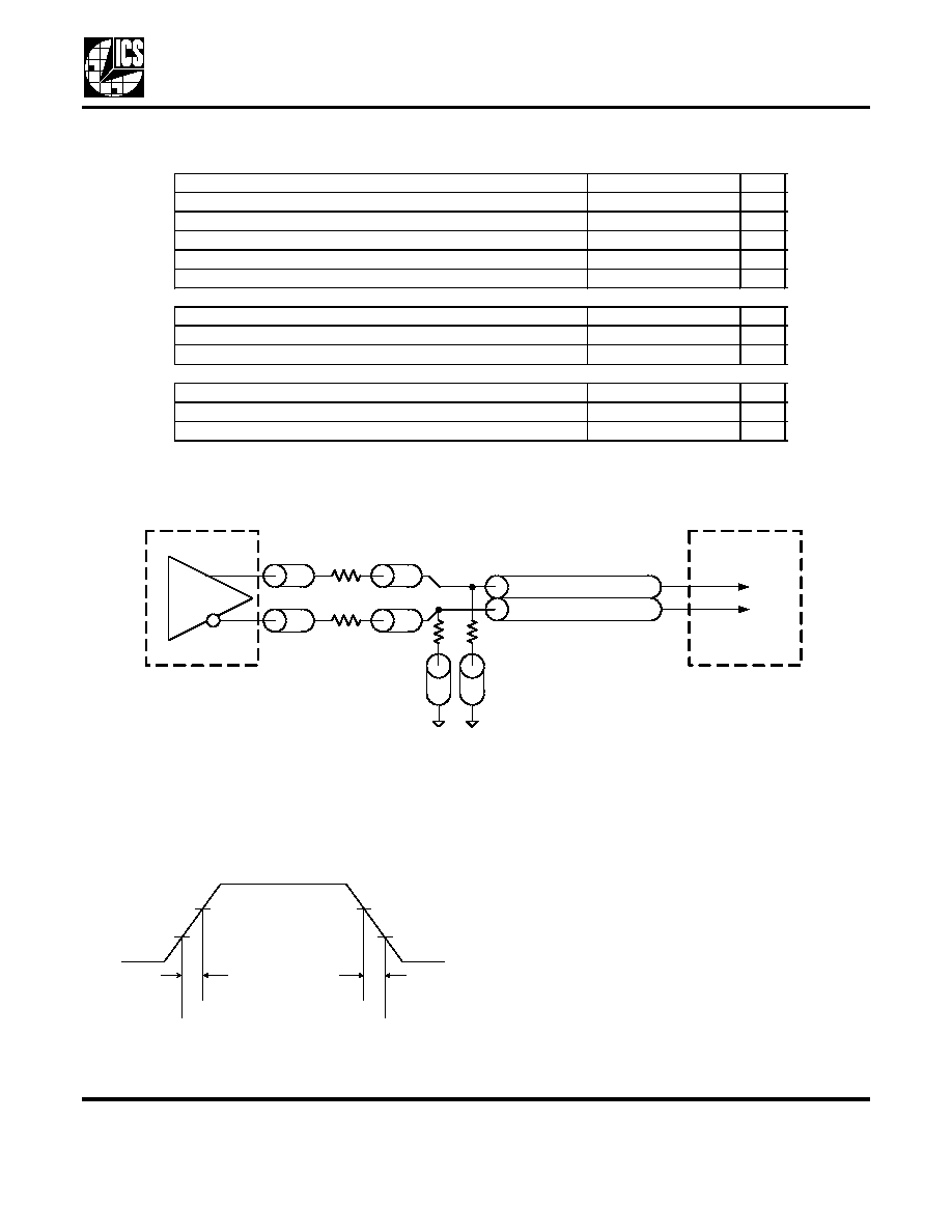
PCI-Express Layout Guidelines
PCI-Express Device Routing
Typical PCI-Express (HCSL)
Waveform
Common Recommendations for Differential Routing
Dimension or Value
Unit
L1 length, Route as non-coupled 50 ohm trace.
0.5 max
inch
L2 length, Route as non-coupled 50 ohm trace.
0.2 max
inch
L3 length, Route as non-coupled 50 ohm trace.
0.2 max
inch
R
S
33
ohm
R
T
49.9
ohm
Differential Routing on a Single PCB
Dimension or Value
Unit
L4 length, Route as coupled microstrip 100 ohm differential trace.
2 min to 16 max
inch
L4 length, Route as coupled stripline 100 ohm differential trace.
1.8 min to 14.4 max
inch
Differential Routing to a PCI Express Connector
Dimension or Value
Unit
L4 length, Route as coupled microstrip 100 ohm differential trace.
0.25 to 14 max
inch
L4 length, Route as coupled stripline 100 ohm differential trace.
0.225 min to 12.6 max inch
R
S
R
S
R
T
R
T
PCI-Express
Load or
Connector
L1
L2
L3'
L4
L1'
L2'
L3
L4'
ICS557-08
Output
Clock
0.175 V
0.525 V
0.175 V
0.525 V
t
OR
t
OF
500 ps
500 ps
700 mV
0
MDS 557-08 C
6
Revision 021606
I n t e gr a t e d C i r c u i t S y s t e m s
5 2 5 R a c e S t r e e t , S a n J o s e, C A 9 5 1 2 6
t e l ( 4 0 8 ) 2 9 7 - 1 2 0 1
w w w. i c s t . c o m
ICS557-08
2:1 Multiplexer Chip for PCI-Express
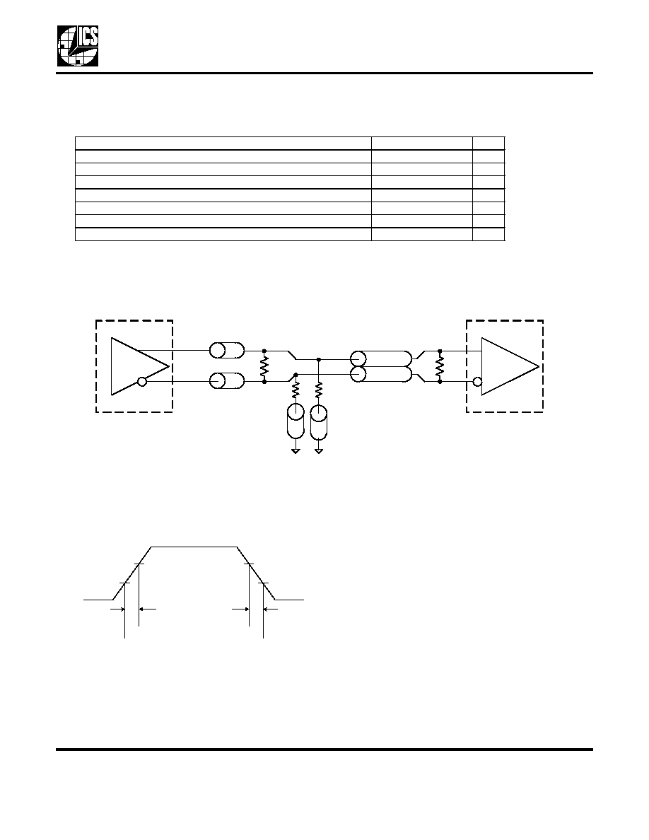
LVDS Compatible Layout Guidelines
LVDS Device Routing
Typical LVDS Waveform
LVDS Recommendations for Differential Routing
Dimension or Value Unit
L1 length, Route as non-coupled 50 ohm trace.
0.5 max
inch
L2 length, Route as non-coupled 50 ohm trace.
0.2 max
inch
R
P
100
ohm
R
Q
100
ohm
R
T
150
ohm
L3 length, Route as coupled 50 ohm differential trace.
L3 length, Route as coupled 50 ohm differential trace.
L1
L2'
L3
L1'
L2
L3'
R
Q
R
P
LVDS
Device
Load
ICS557-08
Clock
Output
R
T
R
T
1150 mV
1250 mV
t
OR
t
OF
500 ps
500 ps
1325 mV
1000 mV
1150 mV
1250 mV
MDS 557-08 C
7
Revision 021606
I n t e gr a t e d C i r c u i t S y s t e m s
5 2 5 R a c e S t r e e t , S a n J o s e, C A 9 5 1 2 6
t e l ( 4 0 8 ) 2 9 7 - 1 2 0 1
w w w. i c s t . c o m
ICS557-08
2:1 Multiplexer Chip for PCI-Express
Absolute Maximum Ratings
Stresses above the ratings listed below can cause permanent damage to the ICS557-08. These ratings are
stress ratings only. Functional operation of the device at these or any other conditions above those
indicated in the operational sections of the specifications is not implied. Exposure to absolute maximum
rating conditions for extended periods can affect product reliability. Electrical parameters are guaranteed
only over the recommended operating temperature range.
DC Electrical Characteristics
Unless stated otherwise, VDD = 3.3 V ±5%, Ambient Temperature -40 to +85
∞C
1
Single edge is monotonic when transitioning through region.
2
Inputs with pull-ups/-downs are not included.
Item
Rating
Supply Voltage, VDD
7 V
All Inputs and Outputs
-0.5 V to VDD+0.5 V
Ambient Operating Temperature
-40 to +85
∞C
Storage Temperature
-65 to +150
∞C
Junction Temperature
125
∞C
Soldering Temperature
260
∞C
ESD Protection (Input)
2000 V min. (HBM)
Parameter
Symbol
Conditions
Min.
Typ.
Max.
Units
Supply Voltage
V
3.135
3.465
V
Input High Voltage
1
V
IH
OE, SEL, PD
2.0
VDD +0.3
V
Input Low Voltage
1
V
IL
OE, SEL, PD
VSS-0.3
0.8
V
Input Leakage Current
2
I
IL
0 < Vin < VDD
-5
5
µA
Operating Supply Current
I
DD
50
, 2 pF
40
mA
I
DDOE
OE =Low
20
mA
I
DDPD
No load, PD =Low
400
µA
Input Capacitance
C
IN
Input pin capacitance
7
pF
Output Capacitance
C
OUT
Output pin capacitance
6
pF
Pin Inductance
L
PIN
5
nH
Output Resistance
R
OUT
CLK outputs
3.0
k
Pull-up Resistor
R
PUP
OE, SEL, PD
110
k
MDS 557-08 C
8
Revision 021606
I n t e gr a t e d C i r c u i t S y s t e m s
5 2 5 R a c e S t r e e t , S a n J o s e, C A 9 5 1 2 6
t e l ( 4 0 8 ) 2 9 7 - 1 2 0 1
w w w. i c s t . c o m
ICS557-08
2:1 Multiplexer Chip for PCI-Express
AC Electrical Characteristics -
Unless stated otherwise, VDD=3.3 V ±5%, Ambient Temperature -40 to +85
∞C
1
Test setup is R
L
=50 ohms with 2 pF, Rr = 475
(1%).
2
Measurement taken from a single-ended waveform.
3
Measurement taken from a differential waveform.
4
Measured at the crossing point where instantaneous voltages of both CLK and CLK are equal.
5
CLK and CLK pins are tri-stated when OE is Low asserted. CLK and CLK are driven differential when OE is High
unless its PD = low.
Parameter
Symbol
Conditions
Min.
Typ.
Max.
Units
Operating Frequency
HCSL termination
200
MHz
LVDS termination
100
MHz
Input High Voltage
1,2
V
IH
HCSL
660
700
850
mV
Input Low Voltage
1,2
V
IL
HCSL
-150
0
mV
Differential Input
Voltages
(V
ID
)
LVDS
250
350
450
mV
Input Offset Voltage
(V
IS
)
LVDS 1.125
1.25
1.375
V
Output High Voltage
1,2
V
OH
HCSL
660
700
850
mV
Output Low Voltage
1,2
V
OL
HCSL
-150
0
mV
Crossing Point
Voltage
1,2
Absolute
250
350
550
mV
Crossing Point
Voltage
1,2,4
Variation over all edges
140
mV
Jitter, Cycle-to-Cycle
1,3
60
ps
Rise Time
1,2
t
OR
From 0.175 V to 0.525 V
175
332
700
ps
Fall Time
1,2
t
OF
From 0.525 V to 0.175 V
175
344
700
ps
Rise/Fall Time
Variation
1,2
125
ps
Duty Cycle
1,3
45
55
%
Output Enable Time
5
All outputs
10
µs
Output Disable Time
5
All outputs
10
µs
Stabilization Time
t
STABLE
From power-up VDD=3.3 V
3.0
ms
Input to Output Delay
Input differential clock to output
differential clock delay measured at
crossing point of input levels to
crossing point of output levels
4
ns

MDS 557-08 C
9
Revision 021606
I n t e gr a t e d C i r c u i t S y s t e m s
5 2 5 R a c e S t r e e t , S a n J o s e, C A 9 5 1 2 6
t e l ( 4 0 8 ) 2 9 7 - 1 2 0 1
w w w. i c s t . c o m
ICS557-08
2:1 Multiplexer Chip for PCI-Express
Thermal Characteristics
Marking Diagram
(ICS557G-08)
Marking Diagram
(ICS557G-08LF)
Marking Diagram
(ICS557GI-08)
Marking Diagram
(ICS557GI-08LF)
Notes:
1. ###### is the lot code.
2. YYWW is the last two digits of the year, and the week number that the part was assembled.
3. "LF" denotes Pb free package.
4. "I" denotes industrial temperature device
5. Bottom marking: (origin). Origin = country of origin if not USA.
Parameter
Symbol
Conditions
Min.
Typ.
Max.
Units
Thermal Resistance Junction to
Ambient
JA
Still air
93
∞C/W
JA
1 m/s air flow
78
∞C/W
JA
3 m/s air flow
65
∞C/W
Thermal Resistance Junction to Case
JC
20
∞C/W
1
8
9
16
557G-08
######
YYWW$$
1
8
9
16
557G08LF
######
YYWW
1
8
9
16
557GI-08
######
YYWW$$
1
8
9
16
557GI08L
######
YYWW
MDS 557-08 C
10
Revision 021606
I n t e gr a t e d C i r c u i t S y s t e m s
5 2 5 R a c e S t r e e t , S a n J o s e, C A 9 5 1 2 6
t e l ( 4 0 8 ) 2 9 7 - 1 2 0 1
w w w. i c s t . c o m
ICS557-08
2:1 Multiplexer Chip for PCI-Express
Package Outline and Package Dimensions
(16-pin TSSOP, 173 Mil. Narrow Body)
Package dimensions are kept current with JEDEC Publication No. 95
Ordering Information
Parts that are ordered with a "LF" suffix to the part number are the Pb-Free configuration and are RoHS compliant.
While the information presented herein has been checked for both accuracy and reliability, Integrated Circuit Systems (ICS)
assumes no responsibility for either its use or for the infringement of any patents or other rights of third parties, which would
result from its use. No other circuits, patents, or licenses are implied. This product is intended for use in normal commercial
applications. Any other applications such as those requiring extended temperature range, high reliability, or other extraordinary
environmental requirements are not recommended without additional processing by ICS. ICS reserves the right to change any
circuitry or specifications without notice. ICS does not authorize or warrant any ICS product for use in life support devices or
critical medical instruments.
Part / Order Number
Marking
Shipping Packaging
Package
Temperature
ICS557G-08
See Page 9
Tubes
16-pin TSSOP
0 to +70
∞ C
ICS557G-08T
Tape and Reel
16-pin TSSOP
0 to +70
∞ C
ICS557G-08LF
Tubes
16-pin TSSOP
0 to +70
∞ C
ICS557G-08LFT
Tape and Reel
16-pin TSSOP
0 to +70
∞ C
ICS557GI-08
See Page 9
Tubes
16-pin TSSOP
-40 to +85
∞ C
ICS557GI-08T
Tape and Reel
16-pin TSSOP
-40 to +85
∞ C
ICS557GI-08LF
Tubes
16-pin TSSOP
-40 to +85
∞ C
ICS557GI-08LFT
Tape and Reel
16-pin TSSOP
-40 to +85
∞ C
INDEX
AREA
1 2
16
D
E1
E
SEATING
PLANE
A1
A
A2
e
- C -
b
aaa
C
c
L
*For reference only. Controlling dimensions in mm.
Millimeters
Inches*
Symbol
Min
Max
Min
Max
A
--
1.20
--
0.047
A1
0.05
0.15
0.002
0.006
A2
0.80
1.05
0.032
0.041
b
0.19
0.30
0.007
0.012
C
0.09
0.20
0.0035
0.008
D
4.90
5.1
0.193
0.201
E
6.40 BASIC
0.252 BASIC
E1
4.30
4.50
0.169
0.177
e
0.65 Basic
0.0256 Basic
L
0.45
0.75
0.018
0.030
0
∞
8
∞
0
∞
8
∞
aaa
--
0.10
--
0.004
MDS 557-08 C
11
Revision 021606
I n t e gr a t e d C i r c u i t S y s t e m s
5 2 5 R a c e S t r e e t , S a n J o s e, C A 9 5 1 2 6
t e l ( 4 0 8 ) 2 9 7 - 1 2 0 1
w w w. i c s t . c o m
ICS557-08
2:1 Multiplexer Chip for PCI-Express
Revision History
Rev.
Originator
Date
Description of Change
C
D.Chan
02/16/06
Added industrial temp range; updated PCI-Express Waveform diagram to include 0.525 V;
changed "Supply Voltage, VDD" spec in Absolute Max. Ratings from 5.5 V to 7 V; changed
CLKOUT to CLK and CLK ; added marking diagrams for I-temp device.