
ICS557-01
MDS 557-01 F
1
Revision 011606
I n t e gra t e d C i r c u i t S y s t e m s
5 2 5 R a c e S t r e e t , S a n J o s e, C A 9 5 1 2 6
t e l ( 4 0 8 ) 2 9 7 - 1 2 0 1
w w w. i c s t . c o m
PCI-E
XPRESS
C
LOCK
S
OURCE
Description
The ICS557-01 is a clock chip designed for use in
PCI-Express Cards as a clock source. It provides a pair
of differential outputs at 100 MHz in a small 8-pin SOIC
package.
Using ICS' patented Phase-Locked Loop (PLL)
techniques, the device takes a 25 MHz crystal input
and produces HCSL (Host Clock Signal Level)
differential outputs at 100 MHz clock frequency. LVDS
signal levels can also be supported via an alternative
termination scheme.
Features
∑
Supports PCI-Express
TM
HCSL Outputs
0.7 V current mode differential pair
∑
Supports LVDS Output Levels
∑
Packaged in 8-pin SOIC
∑
Available in Pb (lead) free package
∑
Operating voltage of 3.3 V
∑
Low power consumption
∑
Input frequency of 25 MHz
∑
Short term jitter 100 ps (peak-to-peak)
∑
Output Enable via pin selection
∑
Industrial temperature range available
Block Diagram
Phase Lock
Loop
Clock
Buffer/
Crystal
Oscillator
VDD
GND
X2
25 MHz
crystal /clock
CLK
OE
CLK
R
R
(IREF)
X1
Crystal Tuning Capacitors

PCI-E
XPRESS
C
LOCK
S
OURCE
MDS 557-01 F
2
Revision 011606
I n t e gr a t e d C i r c u i t S y s t e m s
5 2 5 R a c e S t r e e t , S a n J o s e, C A 9 5 1 2 6
t e l ( 4 0 8 ) 2 9 7 - 1 2 0 1
w w w. i c s t . c o m
ICS557-01
Pin Assignment
Pin Descriptions
1
2
3
X 1
4
X 2
V DD
I RE F
GND
CL K
CL K
8
7
6
5
OE
8 Pi n ( 1 5 0 mi l ) S OI C
Pin
Number
Pin
Name
Pin
Type
Pin Description
1
OE
Input
Output Enable signal
(H = outputs are enabled, L = outputs are disabled/tristated).
Internal pull-up resistor.
2
X1
Input
Crystal or clock input. Connect to a 25 MHz crystal or single ended clock.
3
X2
XO
Crystal Connection. Connect to a parallel mode crystal.
Leave floating if clock input.
4
GND
Power
Connect to ground.
5
IREF
Output
A 475
precision resistor connected between this pin and ground
establishes the external reference current.
6
CLK
Output
HCSL differential complementary clock output.
7
CLK
Output
HCSL differential clock output.
8
VDD
Power
Connect to +3.3 V.

PCI-E
XPRESS
C
LOCK
S
OURCE
MDS 557-01 F
3
Revision 011606
I n t e gr a t e d C i r c u i t S y s t e m s
5 2 5 R a c e S t r e e t , S a n J o s e, C A 9 5 1 2 6
t e l ( 4 0 8 ) 2 9 7 - 1 2 0 1
w w w. i c s t . c o m
ICS557-01
Applications Information
External Components
A minimum number of external components are
required for proper operation.
Decoupling Capacitors
Decoupling capacitors of 0.01
µF should be connected
between VDD and the ground plane (pin 4) as close to
the VDD pin as possible. Do not share ground vias
between components. Route power from power source
through the capacitor pad and then into ICS pin.
Crystal
A 25 MHz fundamental mode parallel resonant crystal
with C
L
= 16 pF should be used. This crystal must have
less than 300 ppm of error across temperature in order
for the ICS557-01 to meet PCI Express specifications.
Crystal Capacitors
Crystal capacitors are connected from pins X1 to
ground and X2 to ground to optimize the accuracy of
the output frequency.
C
L
= Crystal's load capacitance in pF
Crystal Capacitors (pF) = (C
L
- 8) * 2
For example, for a crystal with a 16 pF load cap, each
external crystal cap would be 16 pF. (16-8)*2=16.
Current Source (Iref) Reference Resistor - R
R
If board target trace impedance (Z) is 50
, then R
R
=
475
(1%), providing IREF of 2.32 mA. The output
current (I
OH
) is equal to 6*IREF.
Output Termination
The PCI-Express differential clock outputs of the
ICS557-01 are open source drivers and require an
external series resistor and a resistor to ground. These
resistor values and their allowable locations are shown
in detail in the PCI-Express Layout Guidelines
section.
The ICS557-01can also be configured for LVDS
compatible voltage levels. See the LVDS Compatible
Layout Guidelines section
Output Structures
General PCB Layout Recommendations
For optimum device performance and lowest output
phase noise, the following guidelines should be
observed.
1. Each 0.01µF decoupling capacitor should be
mounted on the component side of the board as close
to the VDD pin as possible.
2. No vias should be used between decoupling
capacitor and VDD pin.
3. The PCB trace to VDD pin should be kept as short
as possible, as should the PCB trace to the ground via.
Distance of the ferrite bead and bulk decoupling from
the device is less critical.
4. An optimum layout is one with all components on the
same side of the board, minimizing vias through other
signal layers (any ferrite beads and bulk decoupling
capacitors can be mounted on the back). Other signal
traces should be routed away from the ICS557-01.This
includes signal traces just underneath the device, or on
layers adjacent to the ground plane layer used by the
device.
R
R
475
6*IREF
=2.3 mA
IREF
See Output Termination
Sections - Pages 3 ~ 5
PCI-E
XPRESS
C
LOCK
S
OURCE
MDS 557-01 F
4
Revision 011606
I n t e gr a t e d C i r c u i t S y s t e m s
5 2 5 R a c e S t r e e t , S a n J o s e, C A 9 5 1 2 6
t e l ( 4 0 8 ) 2 9 7 - 1 2 0 1
w w w. i c s t . c o m
ICS557-01
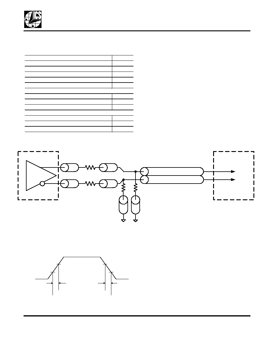
PCI-Express Layout Guidelines
Figure 1: PCI-Express Device Routing
Typical PCI-Express (HCSL)
Waveform
Recommendations for Differential Routing
Dimension
as non-coupled 50 ohm trace.
0.5
as non-coupled 50 ohm trace.
0.2
as non-coupled 50 ohm trace.
0.2
3
49
ferential Routing on a Single PCB
Dimension
as coupled microstrip 100 ohm differential trace.
2 min to
as coupled stripline 100 ohm differential trace.
1.8 min to
ial Routing to a PCI Express Connector
Dimension
as coupled microstrip 100 ohm differential trace.
0.25 to
as coupled stripline 100 ohm differential trace.
0.225 min t
R
S
R
S
R
T
R
T
PCI-Express
Load or
Connector
L1
L2
L3'
L4
L1'
L2'
L3
L4'
ICS557-01
Output
Clock
0.175 V
0.52 V
0.175 V
0.52 V
t
OR
t
OF
500 ps
500 ps
700 mV
0

PCI-E
XPRESS
C
LOCK
S
OURCE
MDS 557-01 F
5
Revision 011606
I n t e gr a t e d C i r c u i t S y s t e m s
5 2 5 R a c e S t r e e t , S a n J o s e, C A 9 5 1 2 6
t e l ( 4 0 8 ) 2 9 7 - 1 2 0 1
w w w. i c s t . c o m
ICS557-01
LVDS Compatible Layout Guidelines
Figure 3: LVDS Device Routing
Typical LVDS Waveform
LVDS Recommendations for Differential Routing
Dimension or Value Unit
L1 length, Route as non-coupled 50 ohm trace.
0.5 max
inch
L2 length, Route as non-coupled 50 ohm trace.
0.2 max
inch
R
P
100
ohm
R
Q
100
ohm
R
T
150
ohm
L3 length, Route as coupled 50 ohm differential trace.
L3 length, Route as coupled 50 ohm differential trace.
L1
L2'
L3
L1'
L2
L3'
R
Q
R
P
LVDS
Device
Load
ICS557-01
Clock
Output
R
T
R
T
1150 mV
1250 mV
t
OR
t
OF
500 ps
500 ps
1325 mV
1000 mV
1150 mV
1250 mV
PCI-E
XPRESS
C
LOCK
S
OURCE
MDS 557-01 F
6
Revision 011606
I n t e gr a t e d C i r c u i t S y s t e m s
5 2 5 R a c e S t r e e t , S a n J o s e, C A 9 5 1 2 6
t e l ( 4 0 8 ) 2 9 7 - 1 2 0 1
w w w. i c s t . c o m
ICS557-01
Absolute Maximum Ratings
Stresses above the ratings listed below can cause permanent damage to the ICS557-01. These ratings are
stress ratings only. Functional operation of the device at these or any other conditions above those
indicated in the operational sections of the specifications is not implied. Exposure to absolute maximum
rating conditions for extended periods can affect product reliability. Electrical parameters are guaranteed
only over the recommended operating temperature range.
DC Electrical Characteristics
Unless stated otherwise, VDD = 3.3 V ±5%, Ambient Temperature -40 to +85
∞C
1
Single edge is monotonic when transitioning through region.
2
Inputs with pull-ups/-downs are not included.
Item
Rating
Supply Voltage, VDD, VDDA
5.5 V
All Inputs and Outputs
-0.5 V to VDD+0.5 V
Ambient Operating Temperature (commercial)
0 to +70
∞C
Ambient Operating Temperature (industrial)
-40 to +85
∞C
Storage Temperature
-65 to +150
∞C
Junction Temperature
125
∞C
Soldering Temperature
260
∞C
ESD Protection (Input)
2000 V min. (HBM)
Parameter
Symbol
Conditions
Min.
Typ.
Max.
Units
Supply Voltage
V
3.135
3.465
Input High Voltage
1
V
IH
2.0
VDD +0.3
V
Input Low Voltage
1
V
IL
VSS-0.3
0.8
V
Input Leakage Current
2
I
IL
0 < Vin < VDD
-5
5
µA
Operating Supply Current
I
DD
With 50
and 2 pF load
55
mA
I
DDOE
OE =Low
35
mA
Input Capacitance
C
IN
Input pin capacitance
7
pF
Output Capacitance
C
OUT
Output pin capacitance
6
pF
Pin Inductance
L
PIN
5
nH
Output Resistance
Rout
CLK outputs
3.0
k
Pull-up Resistor
R
PUP
OE
60
k

PCI-E
XPRESS
C
LOCK
S
OURCE
MDS 557-01 F
7
Revision 011606
I n t e gr a t e d C i r c u i t S y s t e m s
5 2 5 R a c e S t r e e t , S a n J o s e, C A 9 5 1 2 6
t e l ( 4 0 8 ) 2 9 7 - 1 2 0 1
w w w. i c s t . c o m
ICS557-01
AC Electrical Characteristics - CLK/CLK
Unless stated otherwise, VDD=3.3 V ±5%, Ambient Temperature -40 to +85
∞C
1
Test setup is R
L
=50 ohms with 2 pF, R
R
= 475
(1%).
2
Measurement taken from a single-ended waveform.
3
Measurement taken from a differential waveform.
4
Measured at the crossing point where instantaneous voltages of both CLKOUT and CLKOUT are equal.
5
CLKOUT pins are tri-stated when OE is low asserted. CLKOUT is driven differential when OE is high.
Thermal Characteristics
(8-pin SOIC)
Parameter
Symbol
Conditions
Min.
Typ.
Max.
Units
Input Frequency
25
MHz
Output Frequency
100
MHz
Output High Voltage
1,2
V
OH
660
700
850
mV
Output Low Voltage
1,2
V
OL
-150
0
mV
Crossing Point
Voltage
1,2
Absolute
250
350
550
mV
Crossing Point
Voltage
1,2,4
Variation over all edges
140
mV
Jitter, Cycle-to-Cycle
1,3
100
ps
Rise Time
1,2
t
OR
from 0.175 V to 0.525 V
175
332
700
ps
Fall Time
1,2
t
OF
from 0.525 V to 0.175 V
175
344
700
ps
Rise/Fall Time
Variation
1,2
125
ps
Duty Cycle
1,3
45
55
%
Output Enable Time
5
All outputs
30
µs
Output Disable Time
5
All outputs
30
µs
Stabilization Time
t
STABLE
From power-up VDD=3.3 V
3.0
ms
Spread Change Time
t
SPREAD
Settling period after spread change
3.0
ms
Parameter
Symbol
Conditions
Min.
Typ.
Max.
Units
Thermal Resistance Junction to
Ambient
JA
Still air
150
∞C/W
JA
1 m/s air flow
140
∞C/W
JA
3 m/s air flow
120
∞C/W
Thermal Resistance Junction to Case
JC
40
∞C/W

PCI-E
XPRESS
C
LOCK
S
OURCE
MDS 557-01 F
8
Revision 011606
I n t e gr a t e d C i r c u i t S y s t e m s
5 2 5 R a c e S t r e e t , S a n J o s e, C A 9 5 1 2 6
t e l ( 4 0 8 ) 2 9 7 - 1 2 0 1
w w w. i c s t . c o m
ICS557-01
Marking Diagram
(ICS557M-01)
Marking Diagram
(ICS557M-01LF)
Marking Diagram
(ICS557MI-01)
Marking Diagram
(ICS557MI-01LF)
Notes:
1. ###### is the lot code.
2. YYWW is the last two digits of the year, and the week number that the part was assembled.
3. "L" designates Pb (lead) free packaging.
4. Bottom marking: (orgin). Origin = country of origin if not USA.
4
8
5
557M-01
######
YYWW
1
4
8
5
557M-01L
######
YYWW
1
4
8
5
557MI01
######
YYWW
1
4
8
5
557MI01L
######
YYWW
1
PCI-E
XPRESS
C
LOCK
S
OURCE
MDS 557-01 F
9
Revision 011606
I n t e gr a t e d C i r c u i t S y s t e m s
5 2 5 R a c e S t r e e t , S a n J o s e, C A 9 5 1 2 6
t e l ( 4 0 8 ) 2 9 7 - 1 2 0 1
w w w. i c s t . c o m
ICS557-01
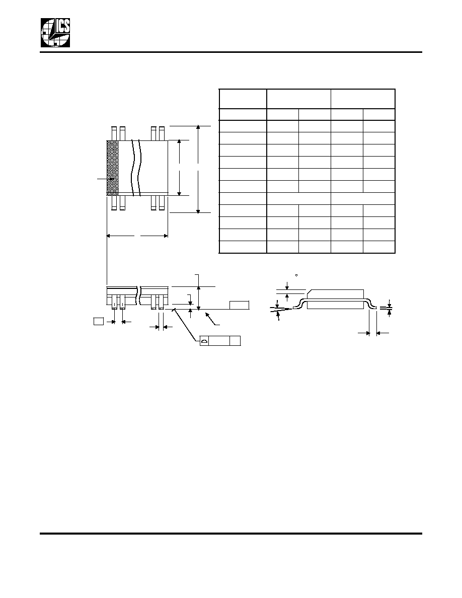
Package Outline and Package Dimensions
(8-pin SOIC, 150 Mil. Narrow Body)
Package dimensions are kept current with JEDEC Publication No. 95
INDEX
AREA
1 2
8
D
E
SEATING
PLANE
A1
A
e
- C -
B
.10 (.004)
C
C
L
H
h x 45
*For reference only. Controlling dimensions in mm.
Millimeters
Inches*
Symbol
Min
Max
Min
Max
A
1.35
1.75
.0532
.0688
A1
0.10
0.25
.0040
.0098
B
0.33
0.51
.013
.020
C
0.19
0.25
.0075
.0098
D
4.80
5.00
.1890
.1968
E
3.80
4.00
.1497
.1574
e
1.27 BASIC
0.050 BASIC
H
5.80
6.20
.2284
.2440
h
0.25
0.50
.010
.020
L
0.40
1.27
.016
.050
0
∞
8
∞
0
∞
8
∞
PCI-E
XPRESS
C
LOCK
S
OURCE
MDS 557-01 F
10
Revision 011606
I n t e gr a t e d C i r c u i t S y s t e m s
5 2 5 R a c e S t r e e t , S a n J o s e, C A 9 5 1 2 6
t e l ( 4 0 8 ) 2 9 7 - 1 2 0 1
w w w. i c s t . c o m
ICS557-01
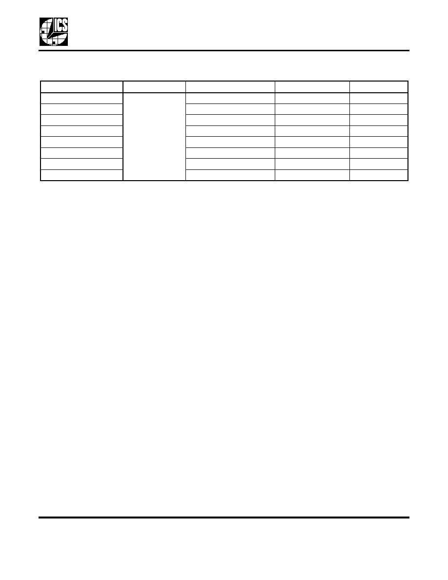
Ordering Information
Parts that are ordered with a "LF" suffix to the part number are the Pb-Free configuration and are RoHS compliant.
While the information presented herein has been checked for both accuracy and reliability, Integrated Circuit Systems (ICS)
assumes no responsibility for either its use or for the infringement of any patents or other rights of third parties, which would
result from its use. No other circuits, patents, or licenses are implied. This product is intended for use in normal commercial
applications. Any other applications such as those requiring extended temperature range, high reliability, or other extraordinary
environmental requirements are not recommended without additional processing by ICS. ICS reserves the right to change any
circuitry or specifications without notice. ICS does not authorize or warrant any ICS product for use in life support devices or
critical medical instruments.
Part / Order Number
Marking
Shipping Packaging
Package
Temperature
ICS557M-01
See Page 8
Tubes
8-pin SOIC
0 to +70
∞ C
ICS557M-01T
Tape and Reel
8-pin SOIC
0 to +70
∞ C
ICS557M-01LF
Tubes
8-pin SOIC
0 to +70
∞ C
ICS557M-01LFT
Tape and Reel
8-pin SOIC
0 to +70
∞ C
ICS557MI-01
Tubes
8-pin SOIC
-40 to +85
∞ C
ICS557MI-01T
Tape and Reel
8-pin SOIC
-40 to +85
∞ C
ICS557MI-01LF
Tubes
8-pin SOIC
-40 to +85
∞ C
ICS557MI-01LFT
Tape and Reel
8-pin SOIC
-40 to +85
∞ C