
ICS558-01
MDS 558-01 C
1
Revision 122105
I n t e gra t e d C i r c u i t S y s t e m s
5 2 5 R a c e S t r e e t , S a n J o s e, C A 9 5 1 2 6
t e l ( 4 0 8 ) 2 9 7 - 1 2 0 1
w w w. i c s t . c o m
PECL/CMOS
TO
CMOS C
LOCK
D
IVIDER
Description
The ICS558-01 accepts a high speed input of either
PECL or CMOS, integrates a divider of 1, 2, 3, or 4, and
provides four CMOS low skew outputs. The chip also
has output enables so that one, three, or all four
outputs can be tri-stated.
The ICS558-01 is a member of the ICS Clock BlocksTM
family of clock generation, synchronization, and
distribution devices.
Features
∑
16-pin TSSOP package
∑
Available in Pb (lead) free package
∑
Selectable PECL or CMOS inputs
∑
Operates up to 250 MHz
∑
Works as a voltage translator
∑
Four low skew (<250 ps) outputs
∑
Selectable internal divider
∑
Operating input voltages of 3.3 V or 5.0 V
∑
Operating output voltages of 2.5 V, 3.3 V or 5.0 V
∑
Ideal for IA64 designs
Block Diagram
OE1
CLK1
CLK2
CLK3
CLK4
PECLIN
Output Divide
PECLIN
S0, S1
GND
VDDP
OE0
GND
VDDC
2
1
0
CMOSIN
SELPECL
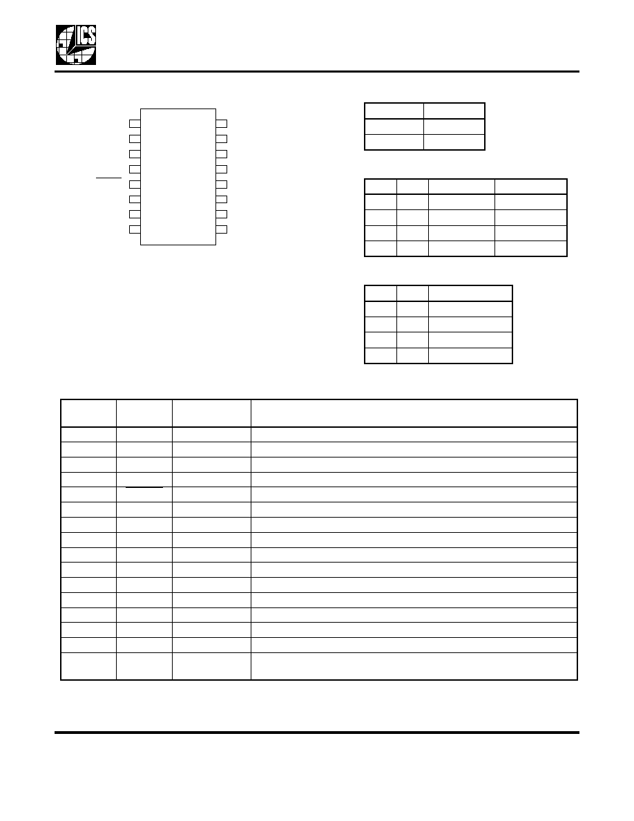
PECL/CMOS
TO
CMOS C
LOCK
D
IVIDER
MDS 558-01 C
2
Revision 122105
I n t e gr a t e d C i r c u i t S y s t e m s
5 2 5 R a c e S t r e e t , S a n J o s e, C A 9 5 1 2 6
t e l ( 4 0 8 ) 2 9 7 - 1 2 0 1
w w w. i c s t . c o m
ICS558-01
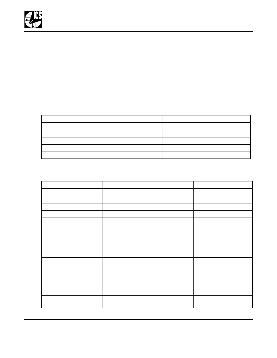
Pin Assignment
Input Clock Selection
Tri-State Table
Output Divide Selection
Pin Descriptions
12
1
11
2
10
3
9
S0
4
S1
5
VDDP
6
VDDC
7
PECLIN
8
PECLIN
CLK1
CLK2
CLK3
GND
CLK4
OE1
CMOSIN
GND
16
15
14
13
OE0
SELPECL
16-pin 173 Mil (0.65mm) TSSOP
SELPECL
Input
0
CMOSIN
1
PECLIN
OE1
OE0
CLK 1
CLK 2, 3, 4
0
0
Tri-state
Tri-state
0
1
Clock ON
Tri-state
1
0
Tri-state
Clock ON
1
1
Clock ON
Clock ON
S1
S0
Output Divide
0
0
/1
0
1
/2
1
0
/3
1
1
/4
Pin
Number
Pin
Name
Pin Type
Pin Description
1
S0
Input
Select 0 for output divider. See table above. Internal pull-up to VDDP.
2
S1
Input
Select 1 for output divider. See table above. Internal pull-up to VDDP.
3
VDDP
Power
Connect to +3.3 V or +5 V. Decouple to pin 6.
4
PECLIN
Clock Input
PECL input. Connect to ground if not used.
5
PECLIN
Clock Input
Complimentary PECL input. Connect to ground if not used.
6
GND
Power
Connect to ground.
7
CMOSIN
Clock Input
CMOS input. Connect to ground if not used.
8
OE0
Input
Output Enable 0. See table above. Internal pull-up to VDDP.
9
OE1
Input
Output Enable 1. See table above. Internal pull-up to VDDP.
10
GND
Power
Connect to ground.
11
CLK4
Output
Low skew clock output.
12
CLK3
Output
Low skew clock output.
13
CLK2
Output
Low skew clock output.
14
CLK1
Output
Low skew clock output.
15
VDDC
Power
Connect to +2.5 V, +3.3 V, or +5 V. Decouple to pin 10.
16
SELPECL
Input
Selects PECL or CMOS input. See table above. Internal pull-up to
VDDP.
PECL/CMOS
TO
CMOS C
LOCK
D
IVIDER
MDS 558-01 C
3
Revision 122105
I n t e gr a t e d C i r c u i t S y s t e m s
5 2 5 R a c e S t r e e t , S a n J o s e, C A 9 5 1 2 6
t e l ( 4 0 8 ) 2 9 7 - 1 2 0 1
w w w. i c s t . c o m
ICS558-01
External Components
The ICS558-01 requires two 0.01
µ
F capacitors between VDDP and GND, and VDDC and GND--one on
each side of the chip. These must be close to the chip to minimize lead inductance. Series termination
resistors of 33
can be used on the outputs (these also must be close to the chip).
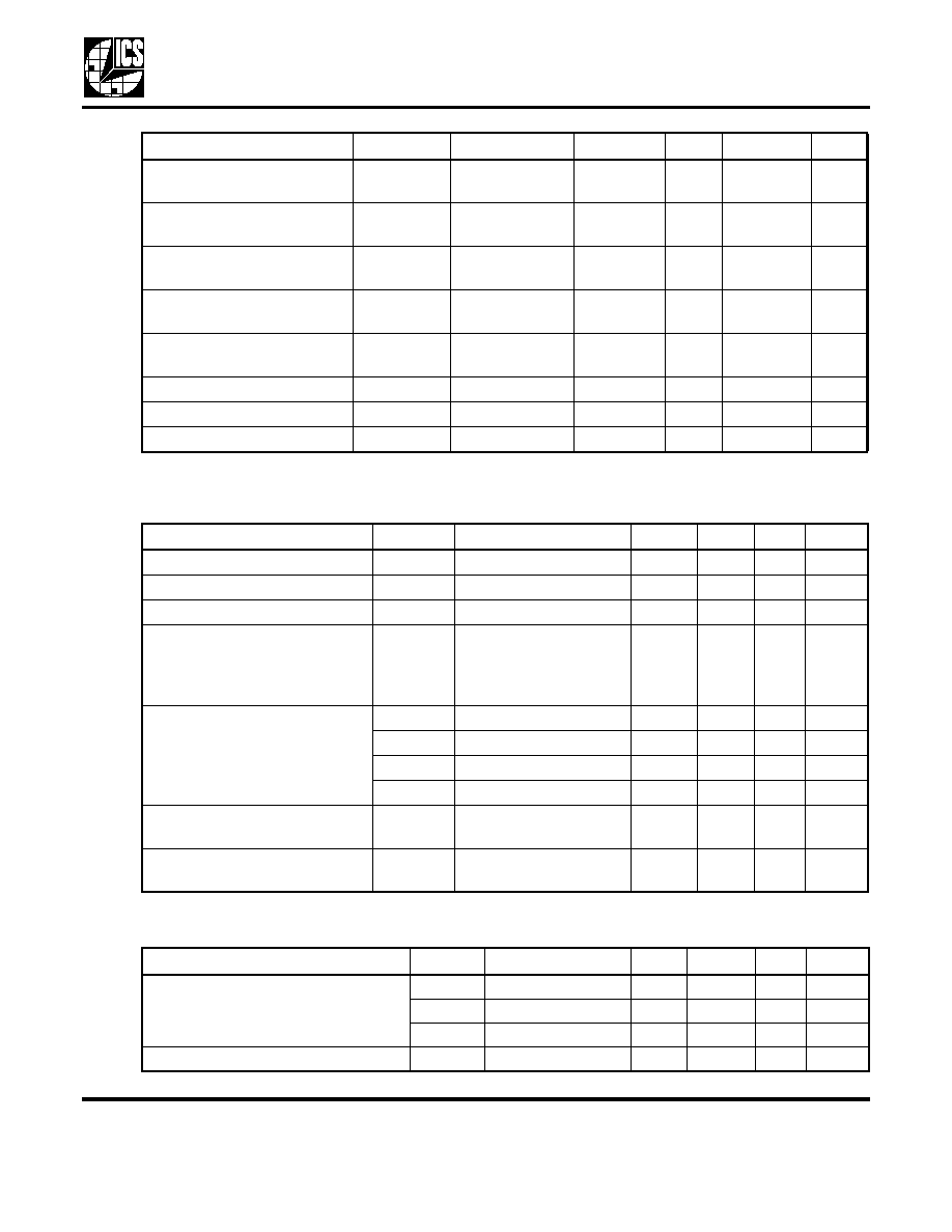
Absolute Maximum Ratings
Stresses above the ratings listed below can cause permanent damage to the ICS558-01. These ratings,
which are standard values for ICS commercially rated parts, are stress ratings only. Functional operation of
the device at these or any other conditions above those indicated in the operational sections of the
specifications is not implied. Exposure to absolute maximum rating conditions for extended periods can
affect product reliability. Electrical parameters are guaranteed only over the recommended operating
temperature range.
DC Electrical Characteristics
VDDP = VDDC = 3.3V (unless stated otherwise), Ambient temperature 0 to +70
∞C
Item
Rating
Supply Voltage; VDDP, VDDC (referenced to ground)
7.0 V
Inputs and Clock Outputs (referenced to ground)
-0.5 V to VDD+0.5 V
Ambient Operating Temperature
0 to +70
∞C
Storage Temperature
-65 to +150
∞C
Soldering Temperature (maximum of 10 seconds)
260
∞C
Parameter
Symbol
Conditions
Min.
Typ.
Max.
Units
Operating Voltage, VDDP
VDDP
VDDC
3.0
5.5
V
Operating Voltage, VDDC
VDDP
VDDC
2.375
VDDP
V
Input High Voltage, CMOSIN
V
IH
(VDDP/2)+1
V
Input Low Voltage, CMOSIN
V
IL
(VDDP/2)-1
V
Input High Voltage
V
IH
non-clock pins
VDDP-0.5
VDDP
V
Input Low Voltage
V
IL
non-clock pins
0.5
V
Common Mode Range,
PECLIN
VDDP=5 V
VDDP-3.7
VDDP-0.6
V
Common Mode Range,
PECLIN
VDDP=3.3 V
VDDP-2.0
VDDP-0.6
V
Peak-to-Peak Input Voltage,
PECLIN
0.3
1.0
V
Output High Voltage
V
OH
VDDC = 5 V,
I
OH
= -24 mA
VDDC-0.4
V
Output Low Voltage
V
OL
VDDC = 5 V,
I
OL
= 24 mA
0.4
V
Output High Voltage
V
OH
VDDC = 3.3 V,
I
OH
= -18 mA
VDDC-0.4
V
PECL/CMOS
TO
CMOS C
LOCK
D
IVIDER
MDS 558-01 C
4
Revision 122105
I n t e gr a t e d C i r c u i t S y s t e m s
5 2 5 R a c e S t r e e t , S a n J o s e, C A 9 5 1 2 6
t e l ( 4 0 8 ) 2 9 7 - 1 2 0 1
w w w. i c s t . c o m
ICS558-01
AC Electrical Characteristics
VDDP = VDDC = 3.3 V (unless stated otherwise), Ambient Temperature 0 to +70
∞C
Thermal Characteristics (16-pin TSSOP)
Output Low Voltage
V
OL
VDDC = 3.3 V,
I
OL
= 18 mA
0.4
V
Output High Voltage
V
OH
VDDC = 2.5 V,
I
OH
= -8 mA
VDDC-0.4
V
Output Low Voltage
V
OL
VDDC = 2.5 V
I
OL
= 8 mA
0.4
V
Operating Supply Current
IDDP
No load, 100
MHz input
22
mA
Operating Supply Current
IDDC
No load, 100
MHz input
18
mA
Short Circuit Current
+70
mA
On-chip pull-up resistor
R
PU
250
k
Input Capacitance
C
IN
4
pF
Parameter
Symbol
Conditions
Min.
Typ.
Max.
Units
Input Frequency
0
250
MHz
Output Rise Time
t
OR
800
ns
Output Fall Time
t
OF
750
ns
Skew, between any output
clocks
(Assumes identically
loaded outputs with
identical rise times,
measured at VDDC/2)
0
250
ps
Propagation Delay
/1
5.0
ns
/2
6.0
ns
/3
ns
/4
7.0
ns
Output Clock Duty Cycle for /2
and /4
45
50
55
%
Output Clock Duty Cycle for /1
and /3
45
50
55
%
Parameter
Symbol
Conditions
Min.
Typ.
Max.
Units
Thermal Resistance Junction to
Ambient
JA
Still air
78
∞C/W
JA
1 m/s air flow
70
∞C/W
JA
3 m/s air flow
68
∞C/W
Thermal Resistance Junction to Case
JC
37
∞C/W
Parameter
Symbol
Conditions
Min.
Typ.
Max.
Units
PECL/CMOS
TO
CMOS C
LOCK
D
IVIDER
MDS 558-01 C
5
Revision 122105
I n t e gr a t e d C i r c u i t S y s t e m s
5 2 5 R a c e S t r e e t , S a n J o s e, C A 9 5 1 2 6
t e l ( 4 0 8 ) 2 9 7 - 1 2 0 1
w w w. i c s t . c o m
ICS558-01
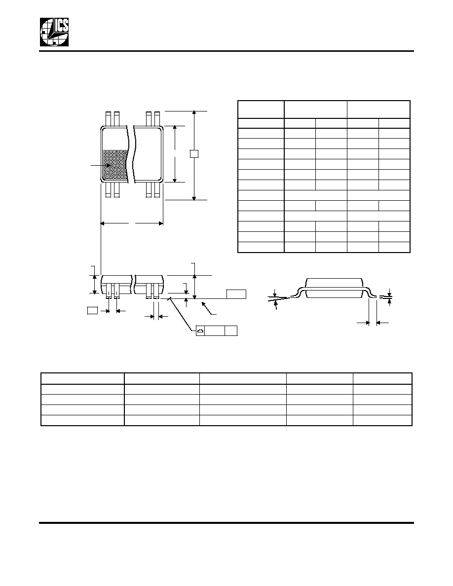
Package Outline and Package Dimensions
(16-pin TSSOP, 4.40 mm Body, 0.65 mm Pitch)
Package dimensions are kept current with JEDEC Publication No. 95, MO-153
Ordering Information
Parts that are ordered with a "LF" suffix to the part number are the Pb-Free configuration and are RoHS compliant.
While the information presented herein has been checked for both accuracy and reliability, Integrated Circuit Systems (ICS)
assumes no responsibility for either its use or for the infringement of any patents or other rights of third parties, which would
result from its use. No other circuits, patents, or licenses are implied. This product is intended for use in normal commercial
applications. Any other applications such as those requiring extended temperature range, high reliability, or other extraordinary
environmental requirements are not recommended without additional processing by ICS. ICS reserves the right to change any
circuitry or specifications without notice. ICS does not authorize or warrant any ICS product for use in life support devices or
critical medical instruments.
Part / Order Number
Marking
Shipping Packaging
Package
Temperature
ICS558G-01
ICS558G-01
Tubes
16-pin TSSOP
0 to +70
∞C
ICS558G-01T
ICS558G-01
Tape and Reel
16-pin TSSOP
0 to +70
∞C
ICS558G-01LF
558G-01LF
Tubes
16-pin TSSOP
0 to +70
∞C
ICS558G-01LFT
558G-01LF
Tape and Reel
16-pin TSSOP
0 to +70
∞C
INDEX
AREA
1 2
16
D
E1
E
SEATING
PLANE
A1
A
A2
e
- C -
b
aaa
C
c
L
Millimeters
Inches
Symbol
Min
Max
Min
Max
A
--
1.20
--
0.047
A1
0.05
0.15
0.002
0.006
A2
0.80
1.05
0.032
0.041
b
0.19
0.30
0.007
0.012
C
0.09
0.20
0.0035
0.008
D
4.90
5.1
0.193
0.201
E
6.40 BASIC
0.252 BASIC
E1
4.30
4.50
0.169
0.177
e
0.65 Basic
0.0256 Basic
L
0.45
0.75
0.018
0.030
0
∞
8
∞
0
∞
8
∞
aaa
--
0.10
--
0.004