 | ÐлекÑÑоннÑй компоненÑ: ICS570A- | СкаÑаÑÑ:  PDF PDF  ZIP ZIP |
Untitled Document
ICS570
MDS 570 E
1
Revision 031403
Integrated Circuit Systems, Inc.
q
525 Race Street, San Jose, CA 95126
q
tel (408) 295-9800
q
www.icst.com
Multiplier and Zero Delay Buffer
Description
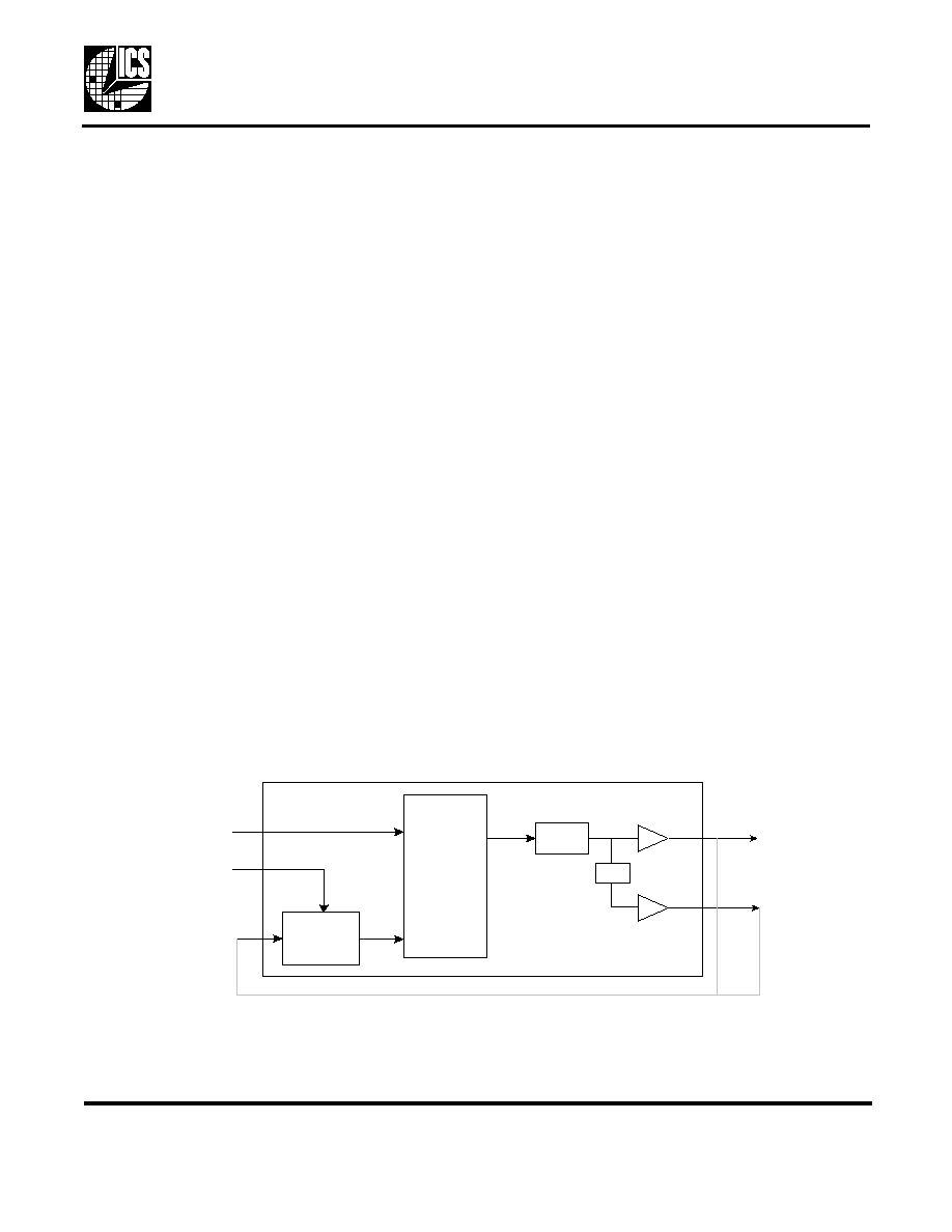
The ICS570 is a high performance Zero Delay Buffer
(ZDB) which integrates ICS' proprietary analog/digital
Phase Locked Loop (PLL) techniques. The A version is
recommended for 5V designs and the B version for
3.3V designs. The chip is part of ICS' ClockBlocks
TM
family, and was designed as a performance upgrade to
meet today's higher speed and lower voltage
requirements. The zero delay feature means that the
rising edge of the input clock aligns with the rising
edges of both output clocks, giving the appearance of
no delay through the device. There are two outputs on
the chip, one being a low-skew divide by two of the
other output. The device incorporates an all-chip power
down/tri-state mode that stops the internal PLL and
puts both outputs into a high impedance state.
The ICS570 is ideal for synchronizing outputs in a large
variety of systems, from personal computers to data
communications to graphics/video. By allowing off-chip
feedback paths, the device can eliminate the delay
through other devices.
The ICS570 A and B versions were designed to
improve input to output jitter from the original ICS570M
version, and are recommended for all new designs.
Features
·
8 pin SOIC package
·
Pin-for-pin replacement and upgrade to ICS570M
·
Functional equivalent to AV9170 (not a pin-for-pin
replacement)
·
Low input to output skew of 300 ps max (>60 MHz
outputs)
·
Ability to choose between 14 different multipliers
from 0.5X to 32X
·
Output clock frequency up to 168 MHz at 3.3V
·
Can recover degraded input clock duty cycle
·
Output clock duty cycle of 45/55
·
Power Down and Tri-State Mode
·
Passes spread spectrum clock modulation
·
Full CMOS clock swings with 25mA drive capability
at TTL levels
·
Advanced, low power CMOS process
·
ICS570B has an operating voltage of 3.3V (±5%)
·
ICS570A has an operating voltage of 5.0V (±5%)
·
Industrial temperature version available
Block Diagram
P h a s e
D e te c to r,
C h a rg e
P u m p ,
a n d L o o p
F ilte r
d ivid e
b y N
C L K
E x te rn a l fe e d b a ck c a n co m e fro m C L K o r C L K /2 (se e ta b le o n p a g e 2 )
IC L K
F B IN
S 1 :0
V C O
C L K 2
/2
Multiplier and Zero Delay Buffer
MDS 570 E
2
Revision 031403
Integrated Circuit Systems, Inc.
q
525 Race Street, San Jose, CA 95126
q
tel (408) 295-9800
q
www.icst.com
ICS570
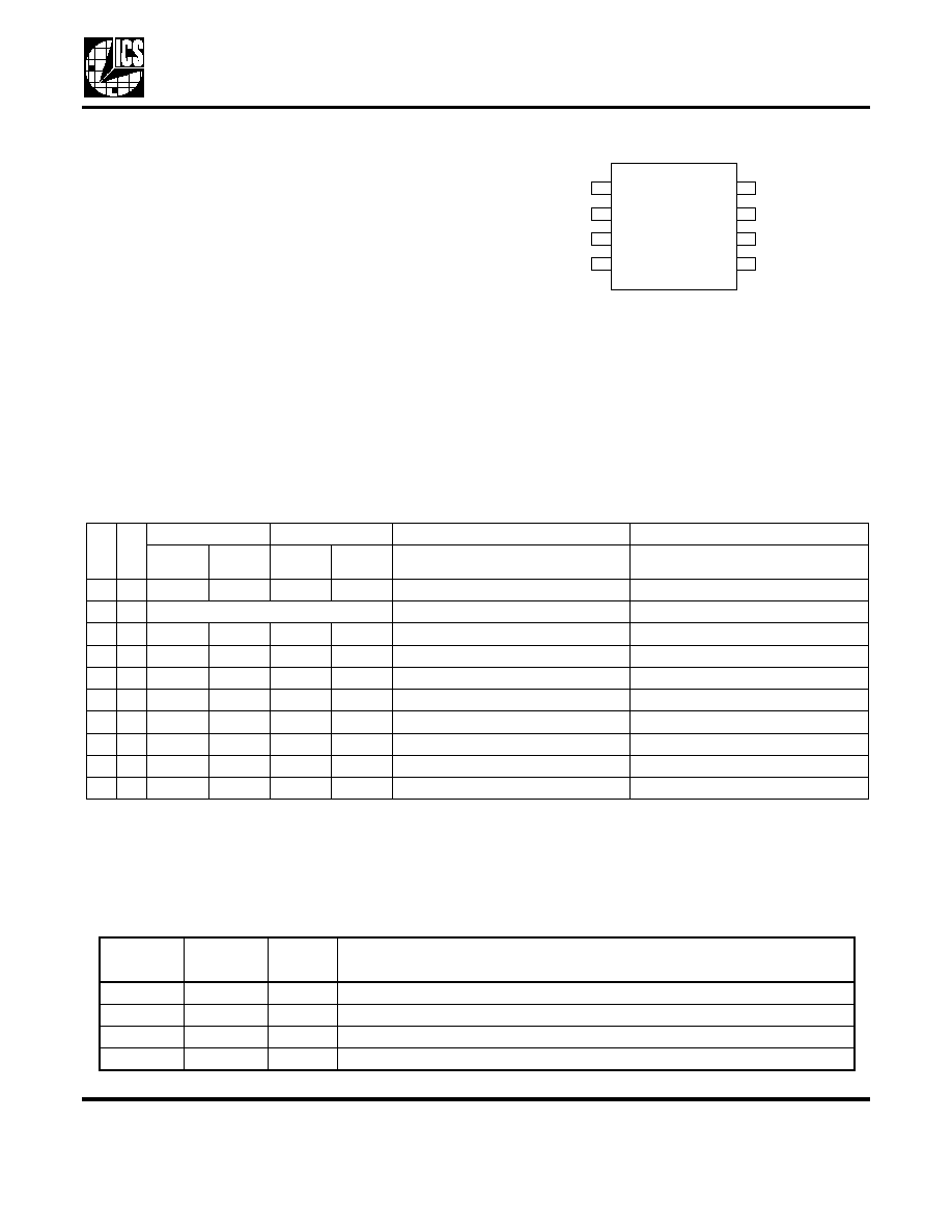
Pin Assignment
Clock Multiplier Decoding Table
(Multiplies Input clock by shown amount)
0 = connect directly to ground
M = leave unconnected (self-biases to VDD/2)
1 = connect directly to VDD
*Input range with CLK feedback is double that for CLK/2
Pin Descriptions
S1
VDD
GND
CLK
ICLK
S0
FBIN
CLK/2
1
2
3
4
8
7
6
5
S1
VDD
GND
CLK
ICLK
S0
FBIN
CLK/2
1
2
3
4
8
7
6
5
8 pin (150 mil) SOIC
S1
S0
FBIN from CLK
FBIN from CLK/2
ICS570B (3.3V)
ICS570A (5.0V)
CLK
CLK2
CLK
CLK2
ICLK Input Range FB from CLK/2*
ICLK Input Range FB from CLK/2*
#1 #6
pin
#7
pin
#8
pin
#7
pin
#8
0
0
Power Down and Tri-State
-
-
0
M
x3
x1.5
x6
x3
3.75 to 28
2.5 to 25
0
1
x4
x2
x8
x4
2.75 to 19
2.5 to 19
M
0
x8
x4
x16
x8
2.5 to 9.5
2.5 to 9.5
M
M
x6
x3
x12
x6
2.5 to 12.5
2.5 to 12.5
M
1
x10
x5
x20
x10
2.5 to 7.5
2.5 to 7.5
1
0
x1
/2
x2
x1
11 to 75
5 to 75
1
M
x16
x8
x32
x16
2.5 to 5
2.5 to 5
1
1
x2
x1
x4
x2
5.5 to 37.5
2.5 to 37.5
Pin
Number
Pin
Name
Pin
Type
Pin Description
1
S1
Input
Select 1 for output clock. Connect to GND, VDD, or float per decoding table above.
2
VDD
Power
Connect to +3.3V (ICS570B). Connect to +5.0V (ICS570A).
3
GND
Power
Connect to ground.
4
ICLK
Input
Reference clock input.
Multiplier and Zero Delay Buffer
MDS 570 E
3
Revision 031403
Integrated Circuit Systems, Inc.
q
525 Race Street, San Jose, CA 95126
q
tel (408) 295-9800
q
www.icst.com
ICS570
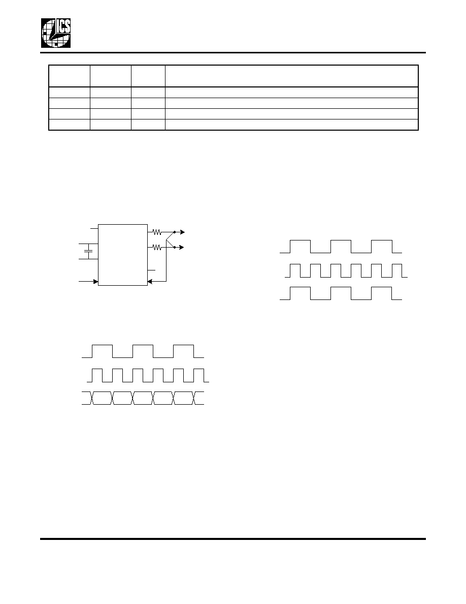
External Components
The ICS570 requires a 0.01µF decoupling capacitor to be connected between VDD and GND. It must be
connected close to the part to minimize lead inductance. No external power supply filtering is required for
this device. A 33
series terminating resistor can be used next to each output pin.
Recommended Circuit
Using CLK as the feedback will always result in synchronized rising edges between ICLK and CLK.
However, the CLK/2 could be a falling edge compared with ICLK. ICS recommends using CLK/2 feedback
whenever possible. This will synchronize the rising edges of all three clocks.
5
FBIN
Input
Feedback clock input.
6
S0
Input
Select 0 for output clock. Connect to GND, VDD, or float per decoding table above.
7
CLK
Output
Clock output per table above.
8
CLK/2
Output
Clock output per table above. Low skew divide by two of pin 7 clock.
Pin
Number
Pin
Name
Pin
Type
Pin Description
CLK
CLK/2
FBIN
S1
VDD
GND
Input
S0
ICLK
x2 Mode (S1, S0 = 1, 1)
CLK Feedback
CLK
CLK/2
ICLK
x2 Mode (S1, S0 = 1, 0)
CLK/2 Feedback
CLK
CLK/2
Multiplier and Zero Delay Buffer
MDS 570 E
4
Revision 031403
Integrated Circuit Systems, Inc.
q
525 Race Street, San Jose, CA 95126
q
tel (408) 295-9800
q
www.icst.com
ICS570
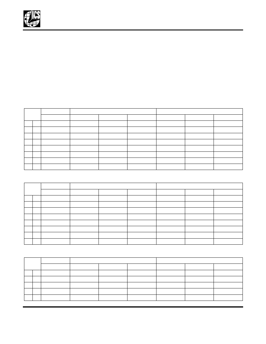
Clock Period Jitter Tables (ICS570A)
All jitter values are considered typical measured at 25
°
C with 27
termination resistor and 15pF loads on
both CLK and CLK/2. The feedback is from CLK/2 to FBIN. Note that if an output is unused, it should be left
unconnected to improve output jitter on the active output clocks.
Absolute and One Sigma Jitter (ps)
Absolute and One Sigma Jitter (ps)
Absolute and One Sigma Jitter (ps)
CLK = 50M
CLK/2 = 25M
S1
S0
CLKIN (MHz)
Multiplier
P to P
1 sigma
Multiplier
P to P
1 sigma
0
M
8.333
6x
±115
80
3x
±65
20
0
1
6.25
8x
±115
80
4x
±60
20
M
0
3.125
16x
±120
80
8x
±55
20
M
M
4.167
12x
±120
90
6x
±60
20
M
1
2.5
20x
±120
80
10x
±60
20
1
0
25
2x
±120
70
1x
±55
20
1
M
1.5625
32x
±120
80
16x
±50
20
1
1
12.5
4x
±120
80
2x
±55
20
CLK = 100M
CLK/2 = 50M
S1
S0
CLKIN (MHz)
Multiplier
P to P
1 sigma
Multiplier
P to P
1 sigma
0
M
16.667
6x
±135
100
3x
±55
20
0
1
12.5
8x
±140
100
4x
±50
20
M
0
6.25
16x
±140
110
8x
±55
20
M
M
8.333
12x
±140
110
6x
±55
20
M
1
5
20x
±135
100
10x
±50
20
1
0
50
2x
±120
90
1x
±50
20
1
M
3.125
32x
±135
100
16x
±55
20
1
1
25
4x
±130
90
2x
±65
20
CLK = 150M
CLK/2 = 75M
S1
S0
CLKIN (MHz)
Multiplier
P to P
1 sigma
Multiplier
P to P
1 sigma
0
M
25
6x
±160
120
3x
±55
20
0
1
18.375
8x
±165
120
4x
±55
20
M
0
9.375
16x
±170
120
8x
±50
20
M
M
12.5
12x
±160
120
6x
±55
20
M
1
7.5
20x
±160
120
10x
±55
20
Multiplier and Zero Delay Buffer
MDS 570 E
5
Revision 031403
Integrated Circuit Systems, Inc.
q
525 Race Street, San Jose, CA 95126
q
tel (408) 295-9800
q
www.icst.com
ICS570
Clock Period Jitter Tables (ICS570B)
All jitter values are considered typical measured at 25
°
C with 27
termination resistor and 15pF loads on
both CLK and CLK/2. The feedback is from CLK/2 to FBIN. Note that if an output is unused, it should be left
unconnected to improve output jitter on the active output clocks.
Absolute and One Sigma Jitter (ps)
Absolute and One Sigma Jitter (ps)
Absolute and One Sigma Jitter (ps)
1
0
75
2x
±155
110
1x
±55
20
1
M
4.6875
32x
±165
120
16x
±55
20
1
1
37.5
4x
±160
110
2x
±50
20
CLK = 50M
CLK/2 = 25M
S1
S0
CLKIN (MHz)
Multiplier
P to P
1 sigma
Multiplier
P to P
1 sigma
0
M
8.333
6x
±110
80
3x
±55
20
0
1
6.25
8x
±125
90
4x
±50
20
M
0
3.125
16x
±130
90
8x
±55
20
M
M
4.167
12x
±120
90
6x
±55
20
M
1
2.5
20x
±115
90
10x
±55
20
1
0
25
2x
±130
50
1x
±55
20
1
M
1.5625
32x
±120
90
16x
±55
20
1
1
12.5
4x
±120
60
2x
±55
20
CLK = 100M
CLK/2 = 50M
S1
S0
CLKIN (MHz)
Multiplier
P to P
1 sigma
Multiplier
P to P
1 sigma
0
M
16.667
6x
±100
70
3x
±45
20
0
1
12.5
8x
±100
70
4x
±45
20
M
0
6.25
16x
±110
80
8x
±45
20
M
M
8.333
12x
±100
70
6x
±45
20
M
1
5
20x
±105
70
10x
±40
20
1
0
50
2x
±90
60
1x
±40
20
1
M
3.125
32x
±95
70
16x
±45
20
1
1
25
4x
±105
70
2x
±60
20
CLK = 150M
CLK/2 = 75M
S1
S0
CLKIN (MHz)
Multiplier
P to P
1 sigma
Multiplier
P to P
1 sigma
0
M
25
6x
±115
70
3x
±50
20
0
1
18.375
8x
±120
80
4x
±50
20
M
0
9.375
16x
±130
90
8x
±50
20
M
M
12.5
12x
±130
90
6x
±45
20
Document Outline