 | –≠–ª–µ–∫—Ç—Ä–æ–Ω–Ω—ã–π –∫–æ–º–ø–æ–Ω–µ–Ω—Ç: ICS570B | –°–∫–∞—á–∞—Ç—å:  PDF PDF  ZIP ZIP |
ICS570B
Multiplier and Zero Delay Buffer
MDS 570B A
1
Revision 053001
Integrated Circuit Systems, Inc . ∑ 525 Race Street ∑ San Jose ∑ CA ∑ 95126 ∑ (408)295-9800tel ∑ www.icst.com
PRELIMINARY INFORMATION
∑ Packaged in 8 pin SOIC.
∑ Pin-for-pin replacement and upgrade to
ICS570/ICS570A
∑ Functional equivalent to AV9170 (not a pin-
for-pin replacement).
∑ Low input to output skew of 300 ps max (>60 MHz
outputs).
∑ Low skew (100 ps) outputs.
∑ Ability to choose between 14 different
multipliers from 0.5X to 32X.
∑ Input clock frequency up to 150 MHz at 3.3V.
∑ Can recover degraded input clock duty cycle.
∑ Output clock duty cycle of 45/55.
∑ Power Down and Tri-State Mode.
∑ Full CMOS clock swings with 25mA drive
capability at TTL levels.
∑ Advanced, low power CMOS process.
∑ Operating voltage of 3.3 V (±5%).
∑ Industrial temperature version available
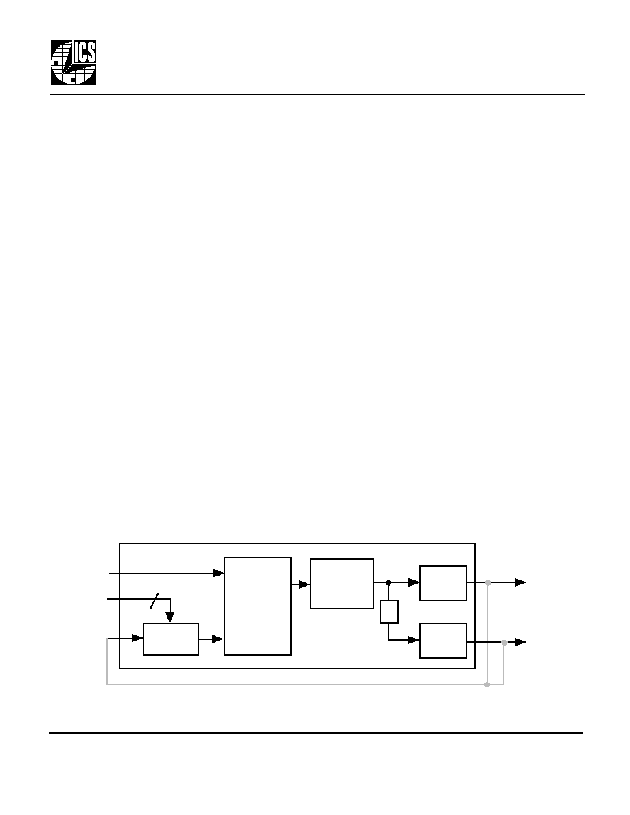
The ICS570B is a high performance Zero Delay Buffer
(ZDB) which integrates ICS' proprietary analog/digital
Phase Locked Loop (PLL) techniques. The ICS570B,
part of ICS' ClockBlocksTM family, was designed as a
performance upgrade to meet today's higher speed and
lower voltage requirements. The zero delay feature
means that the rising edge of the input clock aligns with
the rising edges of both outputs, giving the appearance
of no delay through the device. There are two outputs on
the chip, one being a low-skew divide by two of the other.
The device incorporates an all-chip power down/tri-state
mode that stops the internal PLL and puts both outputs
into a high impedance state.
The ICS570B is ideal for synchronizing outputs in a large
variety of systems, from personal computers to data
communications to graphics/video. By allowing off-chip
feedback paths, the device can eliminate the delay
through other devices.
The ICS570B was done to improve input to output jitter
from the original ICS570M and ICS570A verisons, and is
recommended for all new 3.3 V only designs.
For 5V applications, use the ICS570A.
Block Diagram
Description
Features
divide by N
Phase
Detector,
Charge
Pump, and
Loop Filter
Voltage
Controlled
Oscillator
CLK
Output
Buffer
ICLK
CLK/2
Output
Buffer
FBIN
˜2
S1, S0
2
External feedback can come from CLK or CLK/2 (see table on page 2).
ICS570B
Multiplier and Zero Delay Buffer
MDS 570B A
2
Revision 053001
Integrated Circuit Systems, Inc . ∑ 525 Race Street ∑ San Jose ∑ CA ∑ 95126 ∑ (408)295-9800tel ∑ www.icst.com
PRELIMINARY INFORMATION
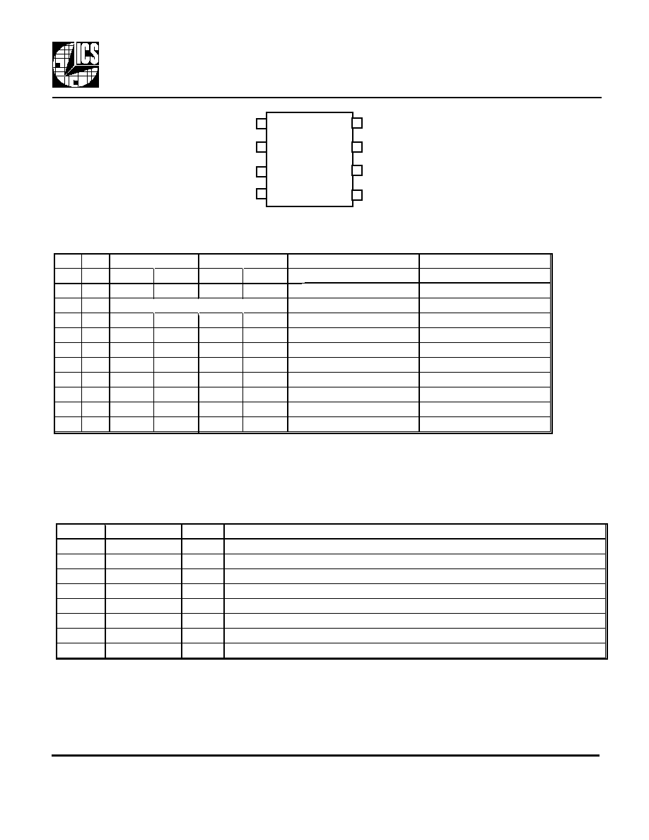
Pin Assignment
Number
Name
Type
Description
1
S1
I
Select 1 for output clock. Connect to GND, VDD, or float per decoding table above.
2
VDD
P
Connect to +3.3V.
3
GND
P
Connect to ground.
4
ICLK
CI
Reference clock input.
5
FBIN
CI
Feedback clock input.
6
S0
I
Select 0 for output clock. Connect to GND, VDD, or float per decoding table above.
7
CLK
O
Clock output per table above.
8
CLK/2
O
Clock output per table above. Low skew divide by two of pin 7 clock.
Pin Descriptions
Key: CI = clock input, I = input, O = output, P = power supply connection
Clock Multiplier Decoding Table
(Multiplies input clock by shown amount)
0 = connect directly to ground.
M = leave unconnected (self-biases to VDD/2).
1 = connect directly to VDD.
*Input range with CLK feedback is double that for CLK/2.
FBIN from CLK
FBIN from CLK
FBIN from CLK/2
FBIN from CLK/2
25∞C ICLK Input Range
85∞C ICLK Input Range
S1
S0
CLK
CLK/2
CLK
CLK/2
FB from CLK/2 *
FB from CLK/2 *
#1
#6
pin # 7
pin # 8
pin # 7
pin # 8
(3.3V, MHz)
(3.3V, MHz)
0
0
Power Down and Tri-State
Power Down and Tri-State
Power Down and Tri-State
Power Down and Tri-State
-
-
0
M
x3
x1.5
x6
x3
2.5 to 25
3 to 25
0
1
x4
x2
x8
x4
2.5 to 19
2.5 to 19
M
0
x8
x4
x16
x8
2.5 to 9.5
2.5 to 9.5
M
M
x6
x3
x12
x6
2.5 to 12.5
2.5 to 12.5
M
1
x10
x5
x20
x10
2.5 to 7.5
2.5 to 7.5
1
0
x1
˜2
x2
x1
5 to 75
8 to 75
1
M
x16
x8
x32
x16
2.5 to 5
2.5 to 5
1
1
x2
x1
x4
x2
2.5 to 37.5
4.5 to 37.5
1
8
2
3
4
7
6
5
S1
GND
CLK
VDD
FBIN
8 pin 150 mil SOIC
ICLK
CLK/2
S0
External Components
The ICS570B requires a 0.01 µF decoupling capacitor to be connected between VDD and GND. It must be
connected close to the ICS570B to minimize lead inductance. No external power supply filtering is required for this
device. A 27
series terminating resistor can be used next to each output pin.
ICS570B
Multiplier and Zero Delay Buffer
MDS 570B A
3
Revision 053001
Integrated Circuit Systems, Inc . ∑ 525 Race Street ∑ San Jose ∑ CA ∑ 95126 ∑ (408)295-9800tel ∑ www.icst.com
PRELIMINARY INFORMATION
Electrical Specifications
Parameter
Conditions
Minimum
Typical
Maximum
Units
ABSOLUTE MAXIMUM RATINGS (Note 1)
ABSOLUTE MAXIMUM RATINGS (Note 1)
Supply Voltage, VDD
Referenced to GND
7
V
Inputs
Referenced to GND
-0.5
VDD+0.5
V
Clock Output
Referenced to GND
-0.5
VDD+0.5
V
Ambient Operating Temperature
ICS570B
0
70
∞C
ICS570BI
-40
85
∞C
Soldering Temperature
Max of 10 seconds
260
∞C
Storage temperature
-65
150
∞C
DC CHARACTERISTICS (VDD = 3.3V)
DC CHARACTERISTICS (VDD = 3.3V)
Operating Voltage, VDD
3.15
3.45
V
Input High Voltage, VIH
ICLK, FBIN
2
V
Input Low Voltage, VIL
ICLK, FBIN
0.8
V
Input High Voltage, VIH
S0, S1
VDD-0.5
V
Input High Voltage, VIM (mid-level)
S0, S1
VDD/2
V
Input Low Voltage, VIL
S0, S1
0.5
V
Output High Voltage, VOH, CMOS level
IOH=-4mA
VDD-0.4
V
Output High Voltage, VOH
IOH=-12mA
2.4
V
Output Low Voltage, VOL
IOL=12mA
0.4
V
IDD Operating Supply Current, 50 in, 100 out
No Load, 3.3V
16
mA
Short Circuit Current
Each Output
±100
mA
Input Capacitance, S1, S0
5
pF
AC CHARACTERISTICS (VDD = 3.3V)
AC CHARACTERISTICS (VDD = 3.3V)
Input Frequency, ICLK (see table on page 2)
FBIN from CLK/2
See Table on Page 2
See Table on Page 2
See Table on Page 2
Output Clock Frequency, CLK
10
150
MHz
Output to output skew
Note 2
100
175
ps
Input to Output Jitter
40-150 MHz
100-250
ps
Input skew, ICLK to FBIN Note 2
CLK>30MHz
-300
300
ps
Input skew, ICLK to FBIN Note 2
VDD=3.3V, CLK<10MHz
-600
600
ps
Output Clock Rise Time, 3.3V
0.8 to 2.0V, note 3
0.75
ns
Output Clock Fall Time, 3.3V
2.0 to 0.8V, note 3
0.75
ns
Output Clock Duty Cycle
at VDD/2
45
49 to 51
55
%
Notes
1. Stresses beyond these can permanently damage the device
2. Assumes clocks with same rise time, measured from rising edges at VDD/2.
3. With 27
terminating resistor and 15 pF loads.

ICS570B
Multiplier and Zero Delay Buffer
MDS 570B A
4
Revision 053001
Integrated Circuit Systems, Inc . ∑ 525 Race Street ∑ San Jose ∑ CA ∑ 95126 ∑ (408)295-9800tel ∑ www.icst.com
PRELIMINARY INFORMATION
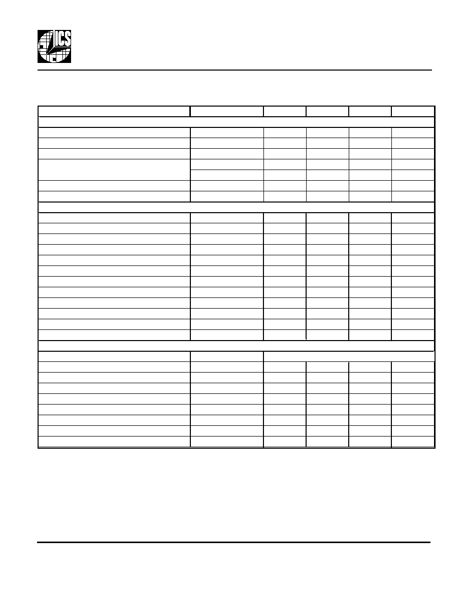
Clock Period Jitter Tables
All jitter values are considered typical measured at 25∞C with 27
series termination resistor and 15pF loads on
both CLK and CLK2. The feedback is from CLK2 to FBIN. Note that if an output is unused, it should be left
unconnected to improve output jitter on the active output clocks.
CLKIN
CLK = 50M
CLK = 50M
CLK = 50M
C L K / 2 = 2 5 M
C L K / 2 = 2 5 M
S 1
S 0
(MHz)
MultiplierAbsolute 1 sigma
Multiplier
Absolute
1 sigma
0
M
8.333
6x
±110
80
3x
±55
20
0
1
6.25
8x
±125
90
4x
±50
20
M
0
3.125
16x
±130
90
8x
±55
20
M
M
4.167
12x
±120
90
6x
±55
20
M
1
2.5
20x
±115
90
10x
±55
20
1
0
25
2x
±130
50
1x
±55
20
1
M
1.5625
32x
±120
90
16x
±55
20
1
1
12.5
4x
±120
60
2x
±55
20
CLKIN
CLK = 100M
CLK = 100M
CLK = 100M
C L K / 2 = 5 0 M
C L K / 2 = 5 0 M
S 1
S 0
(MHz)
MultiplierAbsolute 1 sigma
Multiplier
Absolute
1 sigma
0
M
16.667
6x
±100
70
3x
±45
20
0
1
12.5
8x
±100
70
4x
±45
20
M
0
6.25
16x
±110
80
8x
±45
20
M
M
8.333
12x
±100
70
6x
±45
20
M
1
5
20x
±105
70
10x
±40
20
1
0
50
2x
±90
60
1x
±40
20
1
M
3.125
32x
±95
70
16x
±45
20
1
1
25
4x
±105
70
2x
±60
30
CLKIN
CLK = 150M
CLK = 150M
CLK = 150M
C L K / 2 = 7 5 M
C L K / 2 = 7 5 M
S 1
S 0
(MHz)
MultiplierAbsolute 1 sigma
Multiplier
Absolute
1 sigma
0
M
25
6x
±115
70
3x
±50
20
0
1
18.375
8x
±120
80
4x
±50
20
M
0
9.375
16x
±130
90
8x
±50
20
M
M
12.5
12x
±130
90
6x
±45
20
M
1
7.5
20x
±130
90
10x
±45
20
1
0
75
2x
±115
90
1x
±45
20
1
M
4.6875
32x
±130
90
16x
±50
20
1
1
37.5
4x
±110
70
2x
±60
20
Absolute and One Sigma Jitter (ps), VDD = 3.3V
Absolute and One Sigma Jitter (ps), VDD = 3.3V
Absolute and One Sigma Jitter (ps), VDD = 3.3V
ICS570B
Multiplier and Zero Delay Buffer
MDS 570B A
5
Revision 053001
Integrated Circuit Systems, Inc . ∑ 525 Race Street ∑ San Jose ∑ CA ∑ 95126 ∑ (408)295-9800tel ∑ www.icst.com
PRELIMINARY INFORMATION
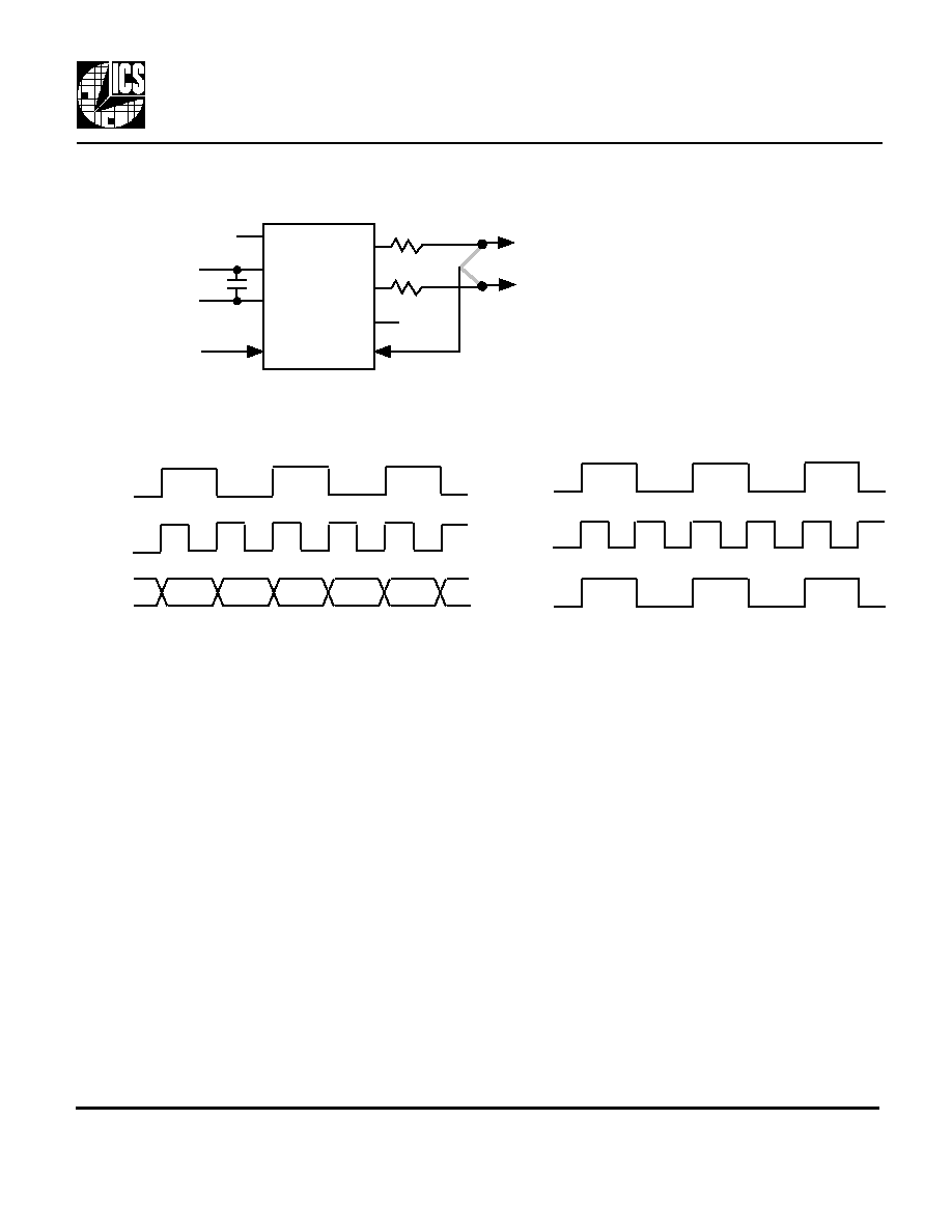
Recommended Circuit:
VDD
GND
INPUT
ICK
CLK
CLK/2
ICLK
CLK
CLK/2
x2 Mode (S1, S0 = 1, 1)
CLK Feedback
x2 Mode (S1, S0 = 1, 0)
CLK/2 Feedback
CLK
CLK/2
S1
S0
Using CLK as the feedback will always result in synchronized rising edges between ICLK and CLK. However, the CLK/2
could be a falling edge compared with ICLK. Therefore, whenever possible, we recommend the use of CLK/2 feedback.
This will synchronize the rising edges of all 3 clocks.
FBIN
ICS570B
Multiplier and Zero Delay Buffer
MDS 570B A
6
Revision 053001
Integrated Circuit Systems, Inc . ∑ 525 Race Street ∑ San Jose ∑ CA ∑ 95126 ∑ (408)295-9800tel ∑ www.icst.com
PRELIMINARY INFORMATION
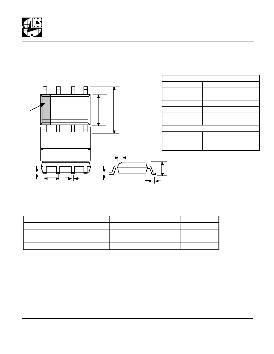
Inches
Inches
Millimeters
Millimeters
Symbol
Min
Max
Min
Max
A
0.0532
0.0688
1.35
1.75
A1
0.004
0.0098
0.10
0.25
B
0.0130
0.0200
0.33
0.51
C
0.0075
0.0098
0.19
0.25
D
0.1890
0.1968
4.80
5.00
E
0.1497
0.1574
3.80
4.00
e
.050 BSC
.050 BSC
1.27 BSC
1.27 BSC
H
0.2284
0.2440
5.80
6.20
h
0.0099
0.0195
0.25
0.50
L
0.0160
0.0500
0.41
1.27
8 pin (150 mil) SOIC
ClockBlocks is a trademark of ICS
Package Outline and Package Dimensions
(For current dimensional specifications, see JEDEC Publication No. 95.)
While the information presented herein has been checked for both accuracy and reliability, Integrated Circuit Systems (ICS) assumes no
responsibility for either its use or for the infringement of any patents or other rights of third parties, which would result from its use. No other
circuits, patents, or licenses are implied. This product is intended for use in normal commercial applications. Any other applications such as those
requiring extended temperature range, high reliability, or other extraordinary environmental requirements are not recommended without additional
processing by ICS. ICS reserves the right to change any circuitry or specifications without notice. ICS does not authorize or warrant any ICS
product for use in life support devices or critical medical instruments.
Ordering Information
Part/Order Number
Marking
Package/Comments
Temperature
ICS570B
ICS570B
8 pin SOIC
0 to 70 ∞C
ICS570BT
ICS570B
8 pin SOIC on tape and reel
0 to 70 ∞C
ICS570BI
ICS570BI
8 pin SOIC
-40 to +85 ∞C
ICS570BIT
ICS570BI
8 pin SOIC on tape and reel
-40 to +85 ∞C
B
D
E
H
e
A1
C
A
h x 45∞
L
INDEX
AREA