 | –≠–ї–µ–Ї—В—А–Њ–љ–љ—Л–є –Ї–Њ–Љ–њ–Њ–љ–µ–љ—В: ICS571 | –°–Ї–∞—З–∞—В—М:  PDF PDF  ZIP ZIP |
ICS571
Low Phase Noise Zero Delay Buffer
MDS 571 B
1
Revision 072899
Printed 11/14/00
Integrated Circuit Systems, Inc.Ј525 Race StreetЈSan JoseЈCAЈ95126Ј(408)295-9800telЈ(408)295-9818fax
PRELIMINARY INFORMATION
Ј Packaged in 8 pin SOIC.
Ј Can function as low phase noise x2 multiplier.
Ј Low skew outputs. One is ч2 of other.
Ј Input clock frequency up to 160 MHz at 3.3V.
Ј Phase noise of better than -100 dBc/Hz from
1kHz to 1MHz offset from carrier
Ј Can recover poor input clock duty cycle.
Ј Output clock duty cycle of 45/55 at 3.3V.
Ј High drive strength for >100 MHz outputs.
Ј Full CMOS clock swings with 25mA drive
capability at TTL levels.
Ј Advanced, low power CMOS process.
Ј Operating voltages of 3.0 to 5.5 V.
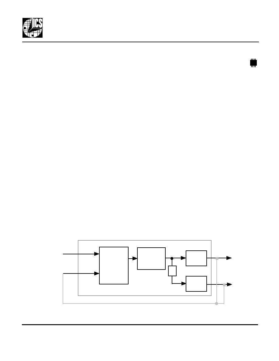
The ICS571 is a high speed, high output drive, low
phase noise Zero Delay Buffer (ZDB) which
integrates ICS' proprietary analog/digital Phase
Locked Loop (PLL) techniques. ICS introduced
the world standard for these devices in 1992 with
the debut of the AV9170, and updated that with
the ICS570. The ICS571, part of ICS'
ClockBlocks
TM
family, was designed to operate at
higher frequencies, with faster rise and fall times,
and with lower phase noise. The zero delay feature
means that the rising edge of the input clock aligns
with the rising edges of both outputs, giving the
appearance of no delay through the device. There
are two outputs on the chip, one being a low-skew
divide by two of the other.
The chip is ideal for synchronizing outputs in a
large variety of systems, from personal computers
to data communications to video. By allowing off-
chip feedback paths, the ICS571 can eliminate the
delay through other devices. The use of dividers in
the feedback path will enable the part to multiply
by more than two.
Block Diagram
Description
Features
Phase
Detector,
Charge
Pump, and
Loop Filter
Voltage
Controlled
Oscillator
CLK
Output
Buffer
ICLK
CLK/2
Output
Buffer
FBIN
ч2
External feedback can come from CLK or CLK/2 (see table on page 2).
ICS571
Low Phase Noise Zero Delay Buffer
MDS 571 B
2
Revision 072899
Printed 11/14/00
Integrated Circuit Systems, Inc.Ј525 Race StreetЈSan JoseЈCAЈ95126Ј(408)295-9800telЈ(408)295-9818fax
PRELIMINARY INFORMATION
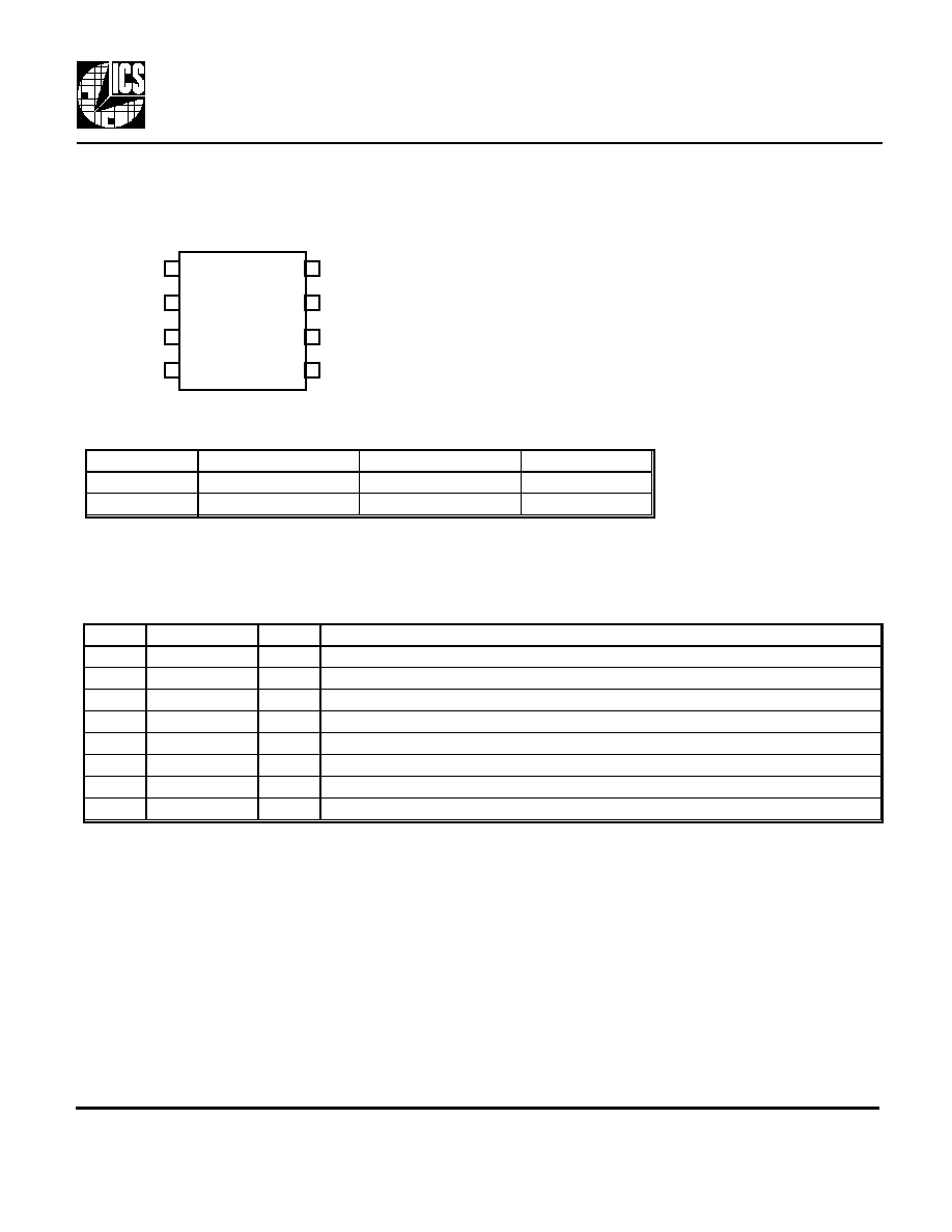
Number
Name
Type
Description
1
ICLK
CI
Reference clock input.
2
VDD
P
Connect to +3.3V or +5V. Must be same as other VDD.
3
GND
P
Connect to ground.
4
CLK/2
O
Clock output per Table above. Low skew divide by two of pin 7 clock.
5
GND
P
Connect to ground.
6
VDD
P
Connect to +3.3V or +5V. Must be same as other VDD.
7
CLK
O
Clock output per Table above.
8
FBIN
CI
Feedback clock input. Connect to CLK or CLK/2 per table above.
Pin Descriptions
Key: CI = clock input, I = input, O = output, P = power supply connection
External Components
The ICS571 requires a 0.01 µF decoupling capacitor to be connected between VDD and GND on each
side of the chip (between pins 2 and 3, and also between pins 6 and 5). They must be connected close to
the ICS571 to minimize lead inductance. No external power supply filtering is required for this device.
A 33
terminating resistor can be used next to each output pin.
Pin Assignment
1
8
2
3
4
7
6
5
ICLK
VDD
GND
CLK/2
FBIN
CLK
VDD
GND
Feedback From
CLK
CLK/2
Input Range
CLK
Input clock frequency
Input clock frequency/2
20 -160 MHz
CLK/2
2xInput clock frequency
Input clock frequency
10 - 80 MHz
Feedback Configuration Table and Frequency Ranges (at 3.3V)
ICS571
Low Phase Noise Zero Delay Buffer
MDS 571 B
3
Revision 072899
Printed 11/14/00
Integrated Circuit Systems, Inc.Ј525 Race StreetЈSan JoseЈCAЈ95126Ј(408)295-9800telЈ(408)295-9818fax
PRELIMINARY INFORMATION
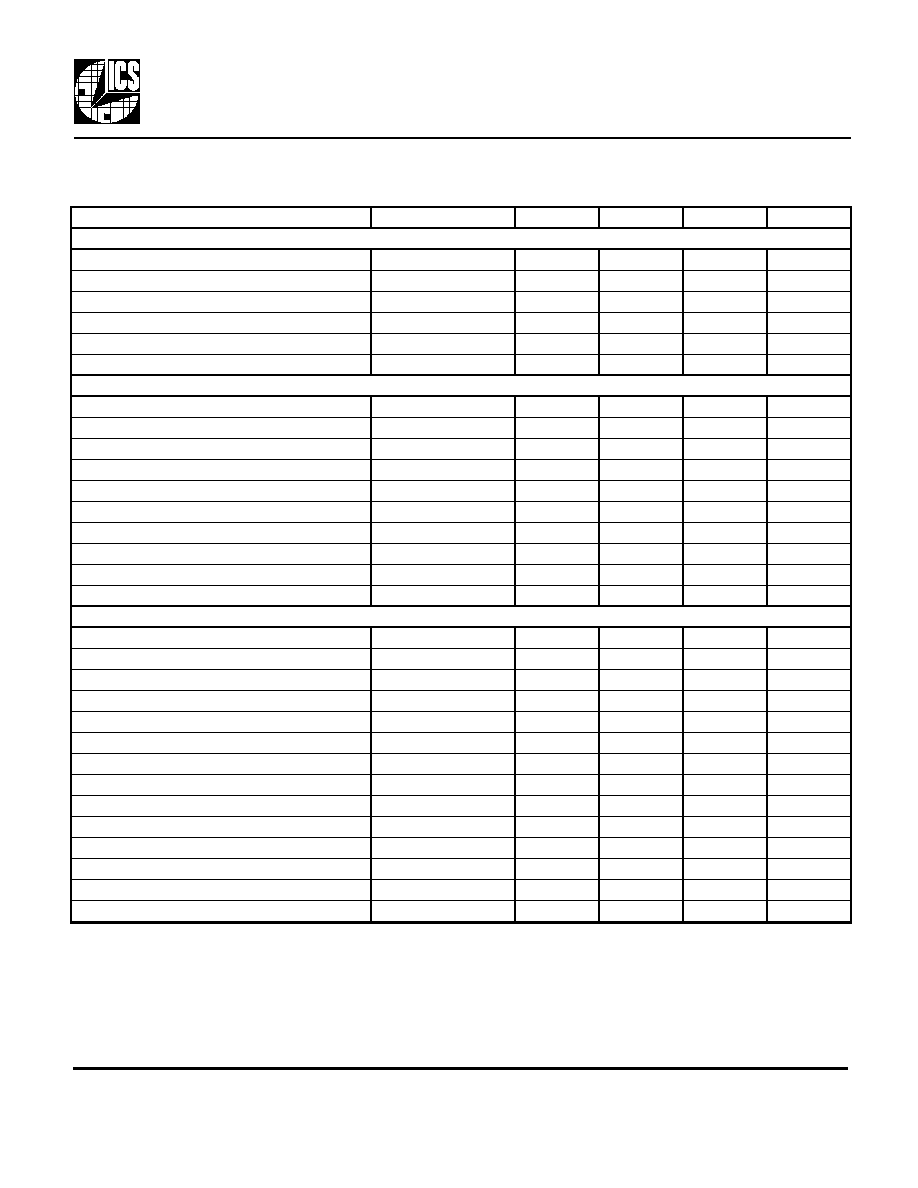
Electrical Specifications
Parameter
Conditions
Minimum
Typical
Maximum
Units
ABSOLUTE MAXIMUM RATINGS (Note 1)
ABSOLUTE MAXIMUM RATINGS (Note 1)
Supply Voltage, VDD
Referenced to GND
7
V
Inputs
Referenced to GND
-0.5
VDD+0.5
V
Clock Output
Referenced to GND
-0.5
VDD+0.5
V
Ambient Operating Temperature
0
70
∞C
Soldering Temperature
Max of 10 seconds
260
∞C
Storage temperature
-65
150
∞C
DC CHARACTERISTICS (VDD = 5.0V or 3.3V unless otherwise noted)
DC CHARACTERISTICS (VDD = 5.0V or 3.3V unless otherwise noted)
DC CHARACTERISTICS (VDD = 5.0V or 3.3V unless otherwise noted)
Operating Voltage, VDD
3
5.5
V
Input High Voltage, VIH, ICLK, FBIN
Pins 1, 8
VDD/2+1
VDD/2
V
Input Low Voltage, VIL, ICLK, FBIN
Pins 1, 8
VDD/2
VDD/2-1
V
Output High Voltage, VOH, CMOS level
IOH=-4mA
VDD-0.4
V
Output High Voltage, VOH
IOH=-25mA
2.4
V
Output Low Voltage, VOL
IOL=25mA
0.4
V
IDD Operating Supply Current, 133 in, 133 out
No Load, 3.3V
34
mA
IDD Operating Supply Current, 50 in, 100 out
No Load, 3.3V
26
mA
Short Circuit Current
Each Output
±100
mA
Input Capacitance, ICLK, FBIN
5
pF
AC CHARACTERISTICS (VDD = 5.0V or 3.3V unless otherwise noted)
AC CHARACTERISTICS (VDD = 5.0V or 3.3V unless otherwise noted)
AC CHARACTERISTICS (VDD = 5.0V or 3.3V unless otherwise noted)
Input Frequency, clock input
FB from CLK
20
160
MHz
Input Frequency, clock input
FB from CLK/2
10
80
MHz
Skew CLK/2 with respect to CLK
Note 2
150
500
850
ps
Input clock to output connected to FBIN
Note 2
-500
500
ps
Output Clock Rise Time, 5V
0.8 to 2.0V, 15 pF load
0.3
ns
Output Clock Fall Time, 5V
2.0 to 0.8V, 15 pF load
0.4
ns
Output Clock Rise Time, 3.3V
0.8 to 2.0V, 15 pF load
0.45
ns
Output Clock Fall Time, 3.3V
2.0 to 0.8V, 15 pF load
0.55
ns
Output Clock Duty Cycle, 5V
at VDD/2
40
52 to 55
60
%
Output Clock Duty Cycle, 3.3V
at VDD/2
45
49 to 51
55
%
Absolute Clock Period Jitter, CLK, note 3
Deviation from mean
±80
ps
One Sigma Clock Period Jitter, CLK, note 3
50
ps
Phase Noise, relative to carrier
1kHz offset
-105
dBc/Hz
Phase Noise, relative to carrier
100kHz offset
-115
dBc/Hz
Notes:
1. Stresses beyond these can permanently damage the device.
2. Assumes clocks with same rise time, measured from rising edges at VDD/2. Measured with 33
termination resistors and 15 pF loads. Applies to both 3.3V and 5V operation.
3. CLK/2 has lower jitter (both absolute and one sigma, in ps) than CLK.

ICS571
Low Phase Noise Zero Delay Buffer
MDS 571 B
4
Revision 072899
Printed 11/14/00
Integrated Circuit Systems, Inc.Ј525 Race StreetЈSan JoseЈCAЈ95126Ј(408)295-9800telЈ(408)295-9818fax
PRELIMINARY INFORMATION
While the information presented herein has been checked for both accuracy and reliability, Integrated Circuit Systems (ICS) assumes no responsibility for either its use or for the
infringement of any patents or other rights of third parties, which would result from its use. No other circuits, patents, or licenses are implied. This product is intended for use in
normal commercial applications. Any other applications such as those requiring extended temperature range, high reliability, or other extraordinary environmental requirements
are not recommended without additional processing by ICS. ICS reserves the right to change any circuitry or specifications without notice. ICS does not authorize or warrant any
ICS product for use in life support devices or critical medical instruments.
Package Outline and Package Dimensions
Inches
Inches
Millimeters
Millimeters
Symbol
Min
Max
Min
Max
A
0.055
0.068
1.397
1.7272
b
0.013
0.019
0.330
0.483
D
0.185
0.200
4.699
5.080
E
0.150
0.160
3.810
4.064
H
0.225
0.245
5.715
6.223
e .050 BSC
.050 BSC
1.27 BSC
1.27 BSC
h
0.015
0.381
L
0.016
0.035
0.406
0.889
Q
0.004
0.01
0.102
0.254
8 pin SOIC
Ordering Information
c
A
b
D
E
H
e
h x 45∞
Q
Pin 1
ClockBlocks is a trademark of ICS
Part/Order Number
Marking
Package
Temperature
ICS571M
ICS571M
8 pin SOIC
0 to 70 ∞C
ICS571MT
ICS571M
8 pin SOIC on tape and reel
0 to 70 ∞C
L