 | –≠–ª–µ–∫—Ç—Ä–æ–Ω–Ω—ã–π –∫–æ–º–ø–æ–Ω–µ–Ω—Ç: ICS581-02 | –°–∫–∞—á–∞—Ç—å:  PDF PDF  ZIP ZIP |
ICS581-01/02
MDS 581-01/02 D
1
Revision 050203
Integrated Circuit Systems, Inc.
q
525 Race Street, San Jose, CA 95126
q
tel (408) 295-9800
q
www.icst.com
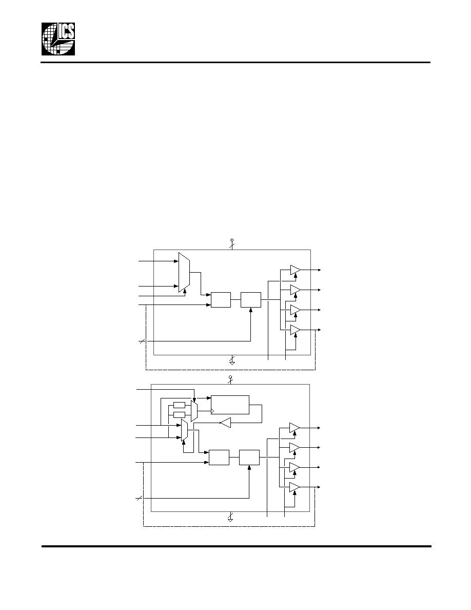
Zero Delay Glitch-Free Clock Multiplexer
Description
The ICS581-01 and ICS581-02 are glitch free, Phase
Locked Loop (PLL) based clock multiplexers (mux) with
zero delay from input to output. They each have four
low skew outputs which can be configured as a single
output, three outputs, or four outputs. The ICS581-01
allows user control over the mux switching, while the
ICS581-02 has automatic switching between the two
clock inputs.
The ICS581-01 and -02 are members of ICS'
ClockBlocks
TM
family of clock generation,
synchronization, and distribution devices. For a
non-PLL based clock mux, see the ICS580-01.
Features
∑
16 pin TSSOP package
∑
No short pulses or glitches on output
∑
Operates from 6 to 200 MHz
∑
Low skew outputs
∑
User controlled (-01) or automatic, timed switch (-02)
∑
Ideal for systems with back-up or redundant clocks
∑
Zero delay, input to output
∑
50% output duty cycle allows duty cycle correction
∑
SpreadSmart
TM
technology works with spread
spectrum parts
∑
Industrial temperature of ICS581-02 available
Block Diagram
PLL
GND
1
0
INA
INB
CLK1
VDD
SELA
Output
Divide
2
S1:0
CLK2
CLK3
CLK4
OE1
FBIN
OE0
2
2
ICS581-01
PLL
GND
INA
INB
CLK1
VDD
Output
Divide
2
S1:0
CLK2
CLK3
CLK4
OE1
FBIN
OE0
2
2
1
0
Transition
Detector
1
0
/3
/48
DIV
IN
ICS581-02
Zero Delay Glitch-Free Clock Multiplexer
MDS 581-01/02 D
2
Revision 050203
Integrated Circuit Systems, Inc.
q
525 Race Street, San Jose, CA 95126
q
tel (408) 295-9800
q
www.icst.com
ICS581-01/02
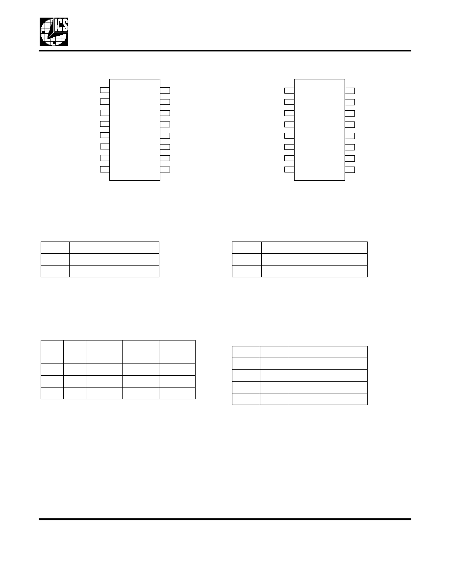
Pin Assignment
Clock Decoding
Tri-State and Power Down
Timeout Selection
Frequency Range Select
12
1
11
2
10
S0
SELA
3
9
S1
4
VDD
VDD
5
INA
6
C LK1
7
INB
8
G ND
C LK2
C LK3
C LK4
FBIN
G N D
O E0
O E1
16
15
14
13
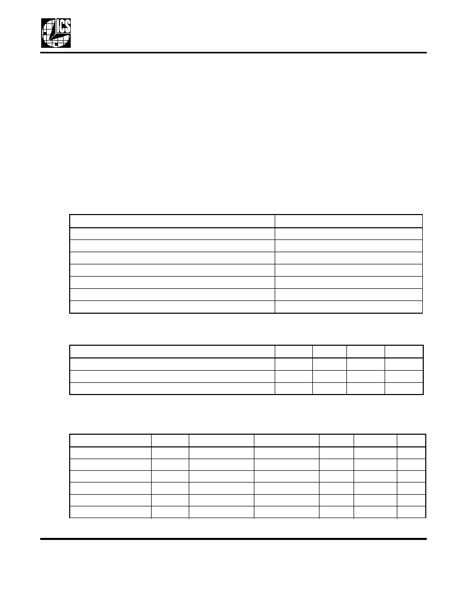
16 pin 4.40 m il body (0.65 m m pitch) T SSO P
IC
S
5
8
1
-
0
1
12
1
11
2
10
S0
D IV
3
9
S1
4
VDD
VDD
5
INA
6
C LK1
7
INB
8
G ND
C LK2
C LK3
C LK4
FBIN
G N D
O E0
O E1
16
15
14
13
16 pin 4.40 m il body (0.65 m m pitch) T SSO P
IC
S
5
8
1
-
0
2
SELA
CLK1-4
0
INB
1
INA
ICS581-01 only
OE1
OE0
CLK1
CLK2-4
PLL
0
0
Z
Z
Off
0
1
On
Z
On
1
0
Z
On
On
1
1
On
On
On
ICS581-01/02
Note: Z indicates that the output is in a high
impedance state
DIV
Nominal Timeout
0
3x period of INB
1
48x period of INB
ICS581-02 only
S1
S0
Input Range (MHz)
0
0
50 - 150
0
1
19 - 75
1
0
6 - 19
1
1
150 - 200
ICS581-01/02
Zero Delay Glitch-Free Clock Multiplexer
MDS 581-01/02 D
3
Revision 050203
Integrated Circuit Systems, Inc.
q
525 Race Street, San Jose, CA 95126
q
tel (408) 295-9800
q
www.icst.com
ICS581-01/02
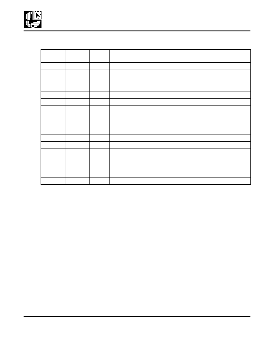
Pin Descriptions
Device Operation
The ICS581-01 and ICS581-02 are very similar.
Following is a description of the operation of the
ICS581-01 and the differences of the ICS581-02.
The ICS581-01 is a PLL-based, zero delay, clock
multiplexer. The device consists of an input multiplexer
controlled by SELA that selects between two clock
inputs. The output of the mux drives the reference input
of a phase locked loop. The other input to the PLL
comes from a feedback input pin called FBIN. The
output of the PLL drives four low skew outputs. These
chip outputs are therefore buffered versions of the
selected input clock with zero delay and 50/50 duty
cycle.
For correct operation, one of the clock outputs must be
connected to FBIN. In this datasheet, CLK4 is shown
as the feedback, but any one of the four clock outputs
can be used. If output termination resistors are used,
the feedback should be connected after the resistor. It
is a property of the PLL used on this chip that it will
align rising edges on FBIN and either INA or INB
(depending on SELA). Since FBIN is connected to a
clock output, this means that the outputs appear to
align with the input with zero delay.
When the input select (SELA) is changed, the output
clock will change frequency and/or phase until it lines
up with the new input clock. This occurs in a smooth,
gradual manner without any short pulses or glitches
and will typically take a few tens of microseconds.
The part must be configured to operate in the correct
frequency range. The table on page two gives the
recommended range.
The four low skew outputs are controlled by two output
enable pins that allow either one, three, or four
simultaneous outputs. If both OE pins are low, the PLL
is powered down.
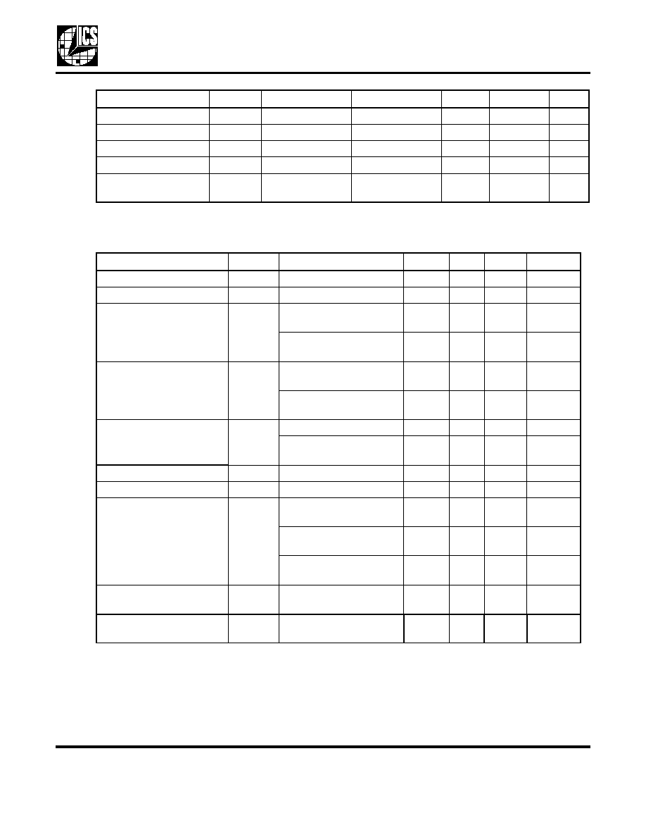
Pin
Number
Pin
Name
Pin
Type
Pin Description
1
S0
Input
Select 0 for frequency range. See table. Internal pull-up.
2
S1
Input
Select 1 for frequency range. See table. Internal pull-up.
3
VDD
Power
Power Supply. Connect to +3.3V or +5V.
4
INA
Input
Input Clock A.
5
INB
Input
Input Clock B.
6
GND
Power
Connect to ground.
7
FBIN
Input
Feedback input. Connect to a clock output.
8
OE0
Input
Output enable 0. See table. Internal pull-up.
9
OE1
Input
Output enable 1. See table. Internal pull-up.
10
GND
Power
Connect to ground.
11
CLK4
Output
Low skew clock output.
12
CLK3
Output
Low skew clock output.
13
CLK2
Output
Low skew clock output.
14
CLK1
Output
Low skew clock output.
15
VDD
Power
Power Supply. Connect to +3.3V or +5V.
16 (-01)
SELA
Input
Mux select. Selects INA when high. Internal pull-up.
16 (-02)
DIV
Input
Timeout select. See table. Internal pull-up.
Zero Delay Glitch-Free Clock Multiplexer
MDS 581-01/02 D
4
Revision 050203
Integrated Circuit Systems, Inc.
q
525 Race Street, San Jose, CA 95126
q
tel (408) 295-9800
q
www.icst.com
ICS581-01/02
Note that the clock driving the FBIN pin must not be
tri-stated unless the PLL is powered down. Otherwise
the PLL will run in an open loop.
The ICS581-02 is identical to the ICS581-01 except for
the switching of the input mux. On the ICS581-02, the
switching is automatically controlled by a transition
detector. The transition detector monitors the clock on
INA. If this clock stops, the output of the detector,
NO_INA goes high, which then selects clock input INB
to the mux. The definition of the clock stopping is
determined by a timeout selected by input DIV. If DIV is
low, NO_INA will go high after no transitions have
occurred on INA for nominally three cycles of the clock
on INB. If DIV is high, the timeout is nominally 48
cycles of INB. When INA restarts, the mux immediately
switches back to the INA selection with no timeout.
Input Clock Frequency
The ICS581-01 and ICS581-02 are designed to switch
between two clocks of the same frequency. They will
also operate with different frequencies on each of the
two input clocks. If the two input frequencies require
different input ranges (see table on page two), then the
highest range should be permanently selected. When
the selected input clock is outside this range, jitter and
input skew specifications may not be met. Consult ICS
for more information.
Application Example
A typical application for the ICS581-02 is to provide a backup clock for a system. The backup reliable clock
would be connected to INB while the main clock would be connected to INA. If the main clock failed, the
ICS581-02 would automatically be switched to the backup clock. The following example shows the
connection for this.
In this example, the clocks are 155 MHz and so the frequency range is address 11. Both S0 and S1 are left
unconnected, causing the on-chip pull-ups to produce the required high inputs. The same is true for OE0,
OE1, and DIV. In this example, CLK4 is used as the feedback. Note that the feedback path is after the
series resistor.
CLK3
S0
CLK4
S1
GND
VDD
OE1
INA
INB
GND
FBIN
OE0
DIV
VDD
CLK1
CLK2
VDD
0.01
µ
F
33
33
33
33
0.01
µ
F
MAIN
BACKUP
Zero Delay Glitch-Free Clock Multiplexer
MDS 581-01/02 D
5
Revision 050203
Integrated Circuit Systems, Inc.
q
525 Race Street, San Jose, CA 95126
q
tel (408) 295-9800
q
www.icst.com
ICS581-01/02
External Components
The ICS581-01 and ICS581-02 require two 0.01
µ
F capacitors between VDD and GND, one on each side
of the chip. These must be close to the chip to minimize lead inductance. Series termination resistors of
33
can be used on the outputs. These should also be close to the chip with the feedback connection after
the resistor.
Absolute Maximum Ratings
Stresses above the ratings listed below can cause permanent damage to the ICS581-01/02. These ratings,
which are standard values for ICS commercially rated parts, are stress ratings only. Functional operation of
the device at these or any other conditions above those indicated in the operational sections of the
specifications is not implied. Exposure to absolute maximum rating conditions for extended periods can
affect product reliability. Electrical parameters are guaranteed only over the recommended operating
temperature range.
Recommended Operation Conditions
DC Electrical Characteristics
Unless stated otherwise, VDD = 3.3V ±5%, Ambient Temperature -40 to +85
∞
C
Item
Rating
Supply Voltage, VDD
7V
All Inputs and Outputs
-0.5V to VDD+0.5V
Ambient Operating Temperature (ICS581-01, ICS581-02)
0 to +70
∞
C
Ambient Operating Temperature (ICS581-01I)
-40 to +85
∞
C
Storage Temperature
-65 to +150
∞
C
Junction Temperature
175
∞
C
Soldering Temperature
260
∞
C
Parameter
Min.
Typ.
Max.
Units
Ambient Operating Temperature (ICS581-01, ICS581-02)
0
+70
∞
C
Ambient Operating Temperature (ICS581-01I)
-40
+85
∞
C
Power Supply Voltage (measured in respect to GND)
+3.0
+5.5
V
Parameter
Symbol
Conditions
Min.
Typ.
Max.
Units
Operating Voltage
VDD
3.0
5.5
V
Supply Current
IDD
100 MHz, no load
26
mA
Input High Voltage
V
IH
Non-clock inputs
2
V
Input Low Voltage
V
IL
Non-clock inputs
0.8
V
Input High Voltage
V
IH
INA, INB, FBIN
(VDD/2)+1
VDD/2
V
Input Low Voltage
V
IL
INA, INB, FBIN
VDD/2
(VDD/2)-1
V
Zero Delay Glitch-Free Clock Multiplexer
MDS 581-01/02 D
6
Revision 050203
Integrated Circuit Systems, Inc.
q
525 Race Street, San Jose, CA 95126
q
tel (408) 295-9800
q
www.icst.com
ICS581-01/02
AC Electrical Characteristics
Unless stated otherwise, VDD = 3.3V ±5%, Ambient Temperature -40 to +85
∞
C
Note 1: Assumes clocks with same rise times, measured at VDD/2
Note 2: Assumes identically loaded outputs with identical rise times, measured at VDD/2. The maximum skew between
any two clocks is 250 ps not 500 ps.
Note 3: Time taken for output to lock to new clock when mux selection changed from INA to INB.
Note 4. With 50 MHz on INA and 150 MHz on INB
Note 5: With 100 MHz on both INA and INB, 180
∞
out of phase
Input Capacitance
C
IN
5
pF
Output High Voltage
V
OH
I
OH
= -12 mA
VDD-0.5
V
Output Low Voltage
V
OL
I
OL
= 12 mA
0.5
V
Short Circuit Current
I
OS
±70
mA
On-chip pull-up
Resistor
R
PU
S1=0, OE1=0,
SELA, DIV pins
250
k
Parameter
Symbol
Conditions
Min.
Typ.
Max.
Units
Input Frequency
f
IN
6
200
MHz
Input Clock Duty Cycle
at VDD/2
30
70
%
Skew
selected input clock to
FBIN, Note 1
-250
0
250
ps
between any output
clocks, Note 2
-250
0
250
ps
Transition Detector
Timeout
ICS581-02 only
DIV = 0
2
3
4
INB
periods
DIV = 1
32
48
64
INB
periods
Frequency Transition
Time
50 to 150 MHz, Note 3, 4
70
200
µ
s
100 to 100 MHz, Note 3,
5
4
10
µ
s
Output Clock Rise Time
0.8V to 2.0V
1
2
ns
Output Clock Fall Time
2.0V to 0.8V
1
2
ns
Output Clock Duty Cycle
less than 133MHz
at VDD/2, no load
45
55
%
greater than 133MHz
at VDD/2, no load
40
60
%
with S0=S1=1
at VDD/2, no load
40
60
%
Absolute Output Clock
Period Jitter
Deviation from mean
±150
ps
One Sigma Output Clock
Period Jitter
40
ps
Parameter
Symbol
Conditions
Min.
Typ.
Max.
Units
Zero Delay Glitch-Free Clock Multiplexer
MDS 581-01/02 D
7
Revision 050203
Integrated Circuit Systems, Inc.
q
525 Race Street, San Jose, CA 95126
q
tel (408) 295-9800
q
www.icst.com
ICS581-01/02
Thermal Characteristics
Marking Diagram
Notes:
1. xxx is either 01, 01I, or 02
2. YYWW is the last two digits of the year and the week
number that the part was assembled
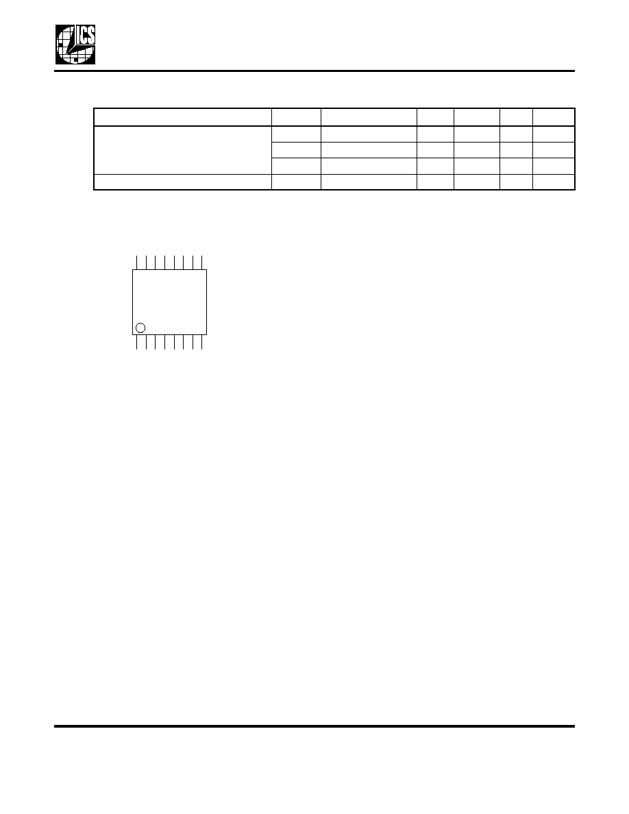
Parameter
Symbol
Conditions
Min.
Typ.
Max.
Units
Thermal Resistance Junction to
Ambient
JA
Still air
78
∞
C/W
JA
1 m/s air flow
70
∞
C/W
JA
3 m/s air flow
68
∞
C/W
Thermal Resistance Junction to Case
JC
37
∞
C/W
ICS
581G-xxx
YYWW$$

Zero Delay Glitch-Free Clock Multiplexer
MDS 581-01/02 D
8
Revision 050203
Integrated Circuit Systems, Inc.
q
525 Race Street, San Jose, CA 95126
q
tel (408) 295-9800
q
www.icst.com
ICS581-01/02
Package Outline and Package Dimensions
(16 pin TSSOP, 4.40 mm Body, 0.65 mm Pitch)
Package dimensions are kept current with JEDEC Publication No. 95, MO-153
Ordering Information
While the information presented herein has been checked for both accuracy and reliability, Integrated Circuit
Systems (ICS) assumes no responsibility for either its use or for the infringement of any patents or other rights of
third parties, which would result from its use. No other circuits, patents, or licenses are implied. This product is
intended for use in normal commercial applications. Any other applications such as those requiring extended
temperature range, high reliability, or other extraordinary environmental requirements are not recommended
without additional processing by ICS. ICS reserves the right to change any circuitry or specifications without notice.
ICS does not authorize or warrant any ICS product for use in life support devices or critical medical instruments.
Part / Order Number
Marking
Shipping
packaging
Package
Temperature
ICS581G-01
ICS581G-01
Tubes
16 pin TSSOP
0 to +70
∞
C
ICS581G-01T
ICS581G-01
Tape and Reel
16 pin TSSOP
0 to +70
∞
C
ICS581G-01I
ICS581G-01I
Tubes
16 pin TSSOP
-40 to +85
∞
C
ICS581G-01IT
ICS581G-01I
Tape and Reel
16 pin TSSOP
-40 to +85
∞
C
ICS581G-02
ICS581G-02
Tubes
16 pin TSSOP
0 to +70
∞
C
ICS581G-02T
ICS581G-02
Tape and Reel
16 pin TSSOP
0 to +70
∞
C
IN D EX
A R E A
1 2
16
D
E 1
E
S E A T IN G
P LA N E
A
1
A
A
2
e
- C -
b
aaa
C
c
L
Millimeters
Inches
Symbol
Min
Max
Min
Max
A
--
1.20
--
0.047
A1
0.05
0.15
0.002
0.006
A2
0.80
1.05
0.032
0.041
b
0.19
0.30
0.007
0.012
C
0.09
0.20
0.0035
0.008
D
4.90
5.1
0.193
0.201
E
6.40 BASIC
0.252 BASIC
E1
4.30
4.50
0.169
0.177
e
0.65 Basic
0.0256 Basic
L
0.45
0.75
0.018
0.030
0
∞
8
∞
0
∞
8
∞
aaa
--
0.10
--
0.004