OE0
ICS581-01, -02
Zero-Delay Glitch-Free Clock Multiplexer
MDS 581-01, 581-02 A
1
Revision 041100
Printed 11/14/00
Integrated Circuit Systems, Inc. ∑ 525 Race Street ∑ San Jose ∑CA∑95126∑ (408) 295-9800tel ∑ www.icst.com
The ICS581-01 and ICS581-02 are glitch free,
Phase Locked Loop (PLL) based clock multiplexers
(mux) with zero delay from input to output. They
each have 4 low skew outputs which can be
configured as a single output, 3 outputs or 4
outputs. The ICS581-01 allows user control over
the mux switching. The ICS581-02 has automatic
switching between the 2 clock inputs.
The ICS581-01 and -02 are members of the ICS
Clock BlocksTM family of clock generation,
synchronization, and distribution devices. For a
non-PLL based clock mux, see the ICS580-01.
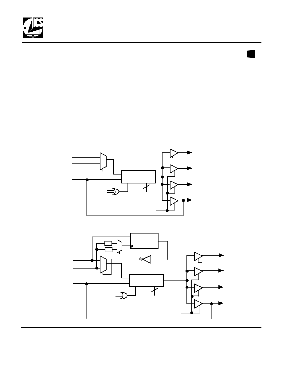
Block Diagrams
Description
Features
∑ Tiny 16 pin TSSOP package
∑ No short pulses or glitches on output. Operates to
200 MHz
∑ User controlled (ICS581-01) or automatic, timed
(ICS581-02) switch
∑ Low skew outputs
∑ Ideal for systems with backup or redundant clocks
∑ Zero delay, input to output
∑ 50% output duty cycle allows duty cycle correction
∑ Spread SmartTM technology works with spread
spectrum parts
PLL
1
0
INA
INB
SELA
FBIN
OE0
OE1
S0, S1
CLK1
CLK2
CLK3
CLK4
OE1
ICS581-01
PLL
1
0
INA
INB
FBIN
OE0
OE1
S0, S1
CLK1
CLK2
CLK3
CLK4
OE1
1
0
˜48
˜3
IN
Transition
Detector
DIV
NO_INA
OE0
ICS581-02
2
External Feedback
External Feedback
2
ICS581-01, -02
Zero-Delay Glitch-Free Clock Multiplexer
MDS 581-01, 581-02 A
2
Revision 041100
Printed 11/14/00
Integrated Circuit Systems, Inc. ∑ 525 Race Street ∑ San Jose ∑CA∑95126∑ (408) 295-9800tel ∑ www.icst.com
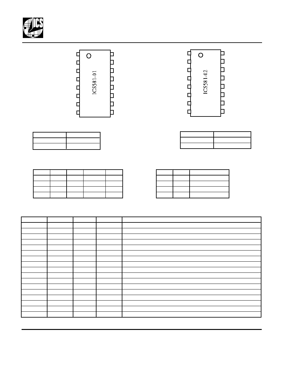
Pin Assignment
1
8
9
16
2
3
4
5
6
7
10
11
12
13
14
15
CLK4
CLK1
VDD
CLK2
CLK3
S0
S1
FBIN
GND
INA
INB
VDD
OE0
GND
SELA
OE1
VDD
1
8
9
16
2
3
4
5
6
7
10
11
12
13
14
15
CLK4
CLK1
VDD
CLK2
CLK3
S0
S1
FBIN
GND
INA
INB
OE0
GND
DIV
OE1
SELA
CLK1:4
0
INB
1
INA
Clock Decoding
ICS581-01 only
DIV
Nominal Timeout
0
3xPeriod of INB
1
48xPeriod of INB
Timeout Selection
ICS581-02 only
Tri-State and Power Down
OE1
OE0
CLK1
CLK2,3,4
PLL
0
0
Z
Z
Off
0
1
On
Z
On
1
0
Z
On
On
1
1
On
On
On
ICS581-01,-02
Pin Descriptions
Key: I = Input; O = output; P = power supply connection
Number
Name
Type
Chip
Description
1
S0
I
-01, -02
Select 0 for frequency range. See table. Internal pull-up.
2
S1
I
-01, -02
Select 1 for frequency range. See table. Internal pull-up.
3
VDD
P
-01, -02
Connect to +3.3 V or + 5 V.
4
INA
I
-01, -02
Input Clock A.
5
INB
I
-01, -02
Input Clock B.
6
GND
P
-01, -02
Connect to ground.
7
FBIN
I
-01, -02
Feedback input. Connect to a clock output.
8
OE0
I
-01, -02
Output Enable0. See Table. Internal pull-up.
9
OE1
I
-01, -02
Output Enable1. See Table. Internal pull-up.
10
GND
P
-01, -02
Connect to ground.
11
CLK4
O
-01, -02
Low skew clock output.
12
CLK3
O
-01, -02
Low skew clock output.
13
CLK2
O
-01, -02
Low skew clock output.
14
CLK1
O
-01, -02
Low skew clock output.
15
VDD
P
-01, -02
Connect to +3.3 V or + 5 V.
16
SELA
I
-01 only
Mux select. Selects INA when high. Internal pull-up.
16
DIV
I
-02 only
Timeout select. See table. Internal pull-up.
S1
S0
Input Range (MHz)
0
0
50-150
0
1
19-75
1
0
6-19
1
1
150-200
Frequency Range Select
ICS581-01,-02

ICS581-01, -02
Zero-Delay Glitch-Free Clock Multiplexer
MDS 581-01, 581-02 A
3
Revision 041100
Printed 11/14/00
Integrated Circuit Systems, Inc. ∑ 525 Race Street ∑ San Jose ∑CA∑95126∑ (408) 295-9800tel ∑ www.icst.com
Device Operation
The ICS581-01 and ICS581-02 are very similar. The following describes the operation of the ICS581-01,
and then the differences of the ICS581-02 will be discussed.
The ICS581-01 is a PLL based, zero delay, clock multiplexer. The device consists of an input multiplexer
controlled by SELA that selects between 2 clock inputs. The output of the mux drives the reference input of
a phase-locked loop. The other input to the PLL comes from a feedback input pin called FBIN. The output
of the PLL drives 4 low skew outputs. These chip outputs are therefore buffered versions of the selected
input clock with zero delay and 50/50 duty cycle.
For correct operation, one of the clock outputs must be connected to FBIN. In this datasheet, CLK4 is
shown as the feedback, but any of the 4 clock outputs can be used. If output termination resistors are used,
the feedback should be connected after the resistor. It is a property of the PLL used on this chip that it will
align rising edges on FBIN and either INA or INB (depending on SELA). Since FBIN is connected to a
clock output, this means that the outputs appear to align with the input with zero delay.
When the input select (SELA) is changed, the output clock will change frequency and/or phase until it lines
up with the new input clock. This occurs in a smooth, gradual manner without any short pulses or glitches,
and will typically take a few tens of microseconds.
The part must be configured to operate in the correct frequency range. The Table on page 2 gives the
recommended range.
The 4 low skew outputs are controlled by 2 output enable pins that allow either 1, 3 or 4 simultaneous
outputs. If both OE pins are low, the PLL is powered down. Note that the clock driving the FBIN pin must
not be tri-stated unless the PLL is powered down, otherwise the PLL will run open loop.
The ICS581-02 is identical to the ICS581-01 except for the switching of the input mux. On the ICS581-
02, the switching is automatically controlled by a transition detector. The transition detector monitors the
clock on INA. If this clock stops, the output of the detector, NO_INA, goes high which then selects clock
input INB to the mux. The definition of the clock stopping is determined by a timeout selected by input
DIV. If DIV is low, NO_INA will go high after no transitions have occurred on INA for nominally 3 cycles
of the clock on INB. If DIV is high the timeout is nominally 48 cycles of INB. When INA restarts, the
mux immediately switches back to the INA selection with no timeout.
Input Clock Frequency
The ICS581-01 and 02 are designed to switch between 2 clocks of the same frequency. They will also
operate with different frequencies on each of the 2 input clocks. If the 2 input frequencies require different
input ranges, (table on page 2) then the highest range should be permanently selected. When the selected
input clock is outside this range, jitter and input skew specifications may not be met. Consult ICS for
more information.

ICS581-01, -02
Zero-Delay Glitch-Free Clock Multiplexer
MDS 581-01, 581-02 A
4
Revision 041100
Printed 11/14/00
Integrated Circuit Systems, Inc. ∑ 525 Race Street ∑ San Jose ∑CA∑95126∑ (408) 295-9800tel ∑ www.icst.com
A typical application for the ICS581-02 is to provide a backup clock for a system. The backup, reliable clock
would be connected to INB while the main clock would be connected to INA. If the main clock failed, the
backup clock would automatically be switched in. The following example shows the connection for this.
S0
S1
VDD
INA
INB
GND
FBIN
OE0
DIV
VDD
CLK1
CLK2
GND
OE1
CLK3
CLK4
VDD
0.01µF
0.01µF
33
In this example, the clocks are 155 MHz and so the frequency range is address 11. Both S0 and S1 are left
unconnected and so the on-chip pull-ups give the required high inputs. Similarly for OE0, OE1 and DIV. In
this example, CLK4 is used as the feedback.
External Components
The ICS581-01 and -02 require two 0.01 µF capacitors between VDD and GND, one on each side of the
chip. These must be close to the chip to minimize lead inductance. Series termination resistors of 33
can
be used on the outputs. These also should be close to the chip, with the feedback connection after the
resistor.
MAIN
BACKUP
Application Example
33
33

ICS581-01, -02
Zero-Delay Glitch-Free Clock Multiplexer
MDS 581-01, 581-02 A
5
Revision 041100
Printed 11/14/00
Integrated Circuit Systems, Inc. ∑ 525 Race Street ∑ San Jose ∑CA∑95126∑ (408) 295-9800tel ∑ www.icst.com
Parameter
Conditions
Minimum
Typical
Maximum
Units
ABSOLUTE MAXIMUM RATINGS
Supply voltage, VDD
Referenced to GND
7
V
Inputs and Clock Outputs
Referenced to GND
-0.5
VDD+0.5
V
Ambient Operating Temperature
0
70
∞C
ICS581G-01I
-40
85
∞C
Soldering Temperature
Max of 10 seconds
260
∞C
Storage temperature
-65
150
∞C
DC CHARACTERISTICS (VDD = 3.3 V unless noted)
DC CHARACTERISTICS (VDD = 3.3 V unless noted)
Operating Voltage, VDD
3.0
5.5
V
Input High Voltage, VIH
INA and INB only
(VDD/2)+1
VDD/2
V
Input Low Voltage, VIL
INA and INB only
VDD/2
(VDD/2)-1
V
Input High Voltage, VIH
Non-clock inputs
2
V
Input Low Voltage, VIL
Non-clock inputs
0.8
V
Output High Voltage, VOH
IOH=-12mA
VDD-0.5
V
Output Low Voltage, VOL
IOL=12mA
0.5
V
Operating Supply Current, IDD
100 MHz inputs, no Load
26
mA
Short Circuit Current
±70
mA
On-chip pull-up resistor
250
k
Input Capacitance
4
pF
AC CHARACTERISTICS (VDD = 3.3 V unless noted)
AC CHARACTERISTICS (VDD = 3.3 V unless noted)
Input Frequency
Note 6
6
200
MHz
Input Clock Duty Cycle
at VDD/2
30
70
%
Skew, selected input clock to FBIN
Note 1
-250
0
250
ps
Skew, between any output clocks
Note 2
-250
0
250
ps
Transition Detector Timeout, DIV=0
ICS581-02 only
2
3
4
INB periods
Transition Detector Timeout, DIV=1
ICS581-02 only
32
48
64
INB periods
Frequency Transition Time, 50 to 150 MHz
Note 3, 4
70
200
µs
Frequency Transition Time, 100 to 100 MHz
Note 3, 5
4
10
µs
Output Clock Rise Time
0.8 V to 2 V
1
2
ns
Output Clock Fall Time
2 V to 0.8 V
1
2
ns
Output Clock Duty Cycle, less than 133 MHz
at VDD/2, no load
45
55
%
Output Clock Duty Cycle, greater than 133 MHz at VDD/2, no load
40
60
%
Output Clock Duty Cycle with S0=S1=1
at VDD/2, no load
40
60
%
Absolute Output Clock Period Jitter
Deviation from mean
±150
ps
One Sigma Output Clock Period Jitter
40
ps
Electrical Specifications
Note 1. Assumes clocks with same rise times, measured at VDD/2.
Note 2. Assumes identically loaded outputs with identical rise times, measured at VDD/2.
The maximum skew between any 2 clocks is 250 ps not 500 ps.
Note 3. Time taken for output to lock to new clock when mux selection changed from INA to INB.
Note 4 With 50 MHz on INA and 150 MHz on INB.
Note 5. With 100 MHz on both INA and INB, 180∞ out of phase.
Note 6. For correct operation, FBIN requires a rail to rail clock. At high frequencies, this may mean that the ICS581 output driving
FBIN cannot drive other loads.

ICS581-01, -02
Zero-Delay Glitch-Free Clock Multiplexer
MDS 581-01, 581-02 A
6
Revision 041100
Printed 11/14/00
Integrated Circuit Systems, Inc. ∑ 525 Race Street ∑ San Jose ∑CA∑95126∑ (408) 295-9800tel ∑ www.icst.com
While the information presented herein has been checked for both accuracy and reliability, Integrated Circuit Systems, Incorporated (ICS) assumes no responsibility for either its
use or for the infringement of any patents or other rights of third parties, which would result from its use. No other circuits, patents, or licenses are implied. This product is
intended for use in normal commercial applications. Any other applications such as those requiring extended temperature range, high reliability, or other extraordinary
environmental requirements are not recommended without additional processing by ICS. ICS reserves the right to change any circuitry or specifications without notice. ICS does
not authorize or warrant any ICS product for use in life support devices or critical medical instruments.
Ordering Information
Part/Order Number
Marking
Shipping, packaging
Package
Temperature
ICS581G-01
ICS581G-01
tubes
16 pin TSSOP
0 to 70 ∞C
ICS581G-01T
ICS581G-01
tape and reel
16 pin TSSOP
0 to 70 ∞C
ICS581G-02
ICS581G-02
tubes
16 pin TSSOP
0 to 70 ∞C
ICS581G-02T
ICS581G-02
tape and reel
16 pin TSSOP
0 to 70 ∞C
ICS581G-01I
ICS581G-01I
tubes
16 pin TSSOP
-40 to 85∞
Package Outline and Package Dimensions
(
For current dimensional specifications, see JEDEC Publication No. 95.)
b
D
E1
E
e
A1
c
A
L
INDEX
AREA
1
2
Inches
Inches
Millimeters
Millimeters
Symbol
Min
Max
Min
Max
A
--
0.047
--
1.19
A1
0.002
0.006
0.05
0.15
b
0.007
0.012
0.18
0.30
c
0.0035
0.008
0.09
0.20
D
0.193
0.201
4.90
5.11
e .025 BSC
.025 BSC
0.65 BSC
0.65 BSC
E .252 BSC
.252 BSC
6.40 BSC
6.40 BSC
E1
0.169
0.177
4.29
4.50
L
0.018
0.030
0.46
0.76
16 pin TSSOP