ICS601-01
MDS 601-01 L
1
Revision 111204
I n t e gra t e d C i r c u i t S y s t e m s
5 2 5 R a c e S t r e e t , S a n J o s e, C A 9 5 1 2 6
t e l ( 4 0 8 ) 2 9 7 - 1 2 0 1
w w w. i c s t . c o m
L
OW
P
HASE
N
OISE
C
LOCK
M
ULTIPLIER
Description
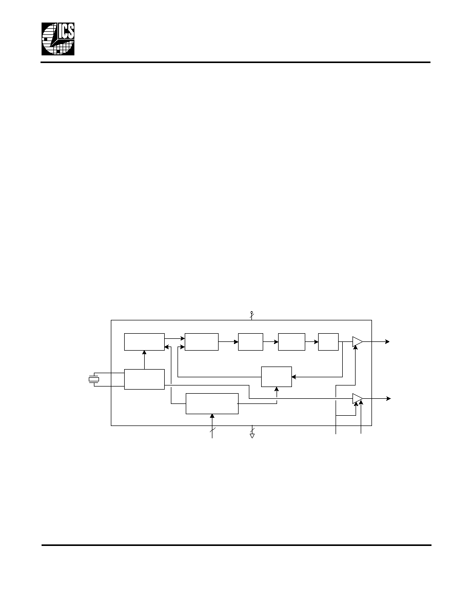
The ICS601-01 is a low-cost, low phase noise,
high-performance clock synthesizer for applications
which require low phase noise and low jitter. It is ICS'
lowest phase noise multiplier, and also the lowest
CMOS part in the industry. Using ICS' patented
analong and digital Phase-Locked Loop (PLL)
techniques, the chip accepts a 10 - 27 MHz crystal or
clock input, and produces output clocks up to 156 MHz
at 3.3 V.
This product is intended for clock generation. It has low
output jitter (variation in the output period), but input
and output skew and jitter are not defined nor
guaranteed. For applications which require definted
input to output timing, use the ICS670-01.
Features
∑
Packaged in 16-pin SOIC or TSSOP
∑
Available in Pb (lead) free package
∑
Uses fundamental 10 - 27 MHz crystal or clock
∑
Patented PLL with the lowest phase noise
∑
Output clocks up to 156 MHz at 3.3 V
∑
Low phase noise: -132 dBc/Hz at 10 kHz
∑
Low jitter - 18 ps one sigma typ.
∑
Full swing CMOS outputs with 25 mA drive capability
at TTL levels
∑
Advanced, low power, sub-micron CMOS process
∑
Industrial temperature range available
∑
Operating voltage of 3.3V or 5V
Block Diagram
ROM Based
Multipliers
VCO
Divide
X1/ICLK
X2
Crystal or
clock input
Crystal
Oscillator
Reference
Divider
Phase
Comparator
Charge
Pump
Loop
Filter
VCO
S3:0
GND
3
4
VDD
3
CLK
REFOUT
REFEN
OE

L
OW
P
HASE
N
OISE
C
LOCK
M
ULTIPLIER
MDS 601-01 L
2
Revision 111204
I n t e gr a t e d C i r c u i t S y s t e m s
5 2 5 R a c e S t r e e t , S a n J o s e, C A 9 5 1 2 6
t e l ( 4 0 8 ) 2 9 7 - 1 2 0 1
w w w. i c s t . c o m
ICS601-01
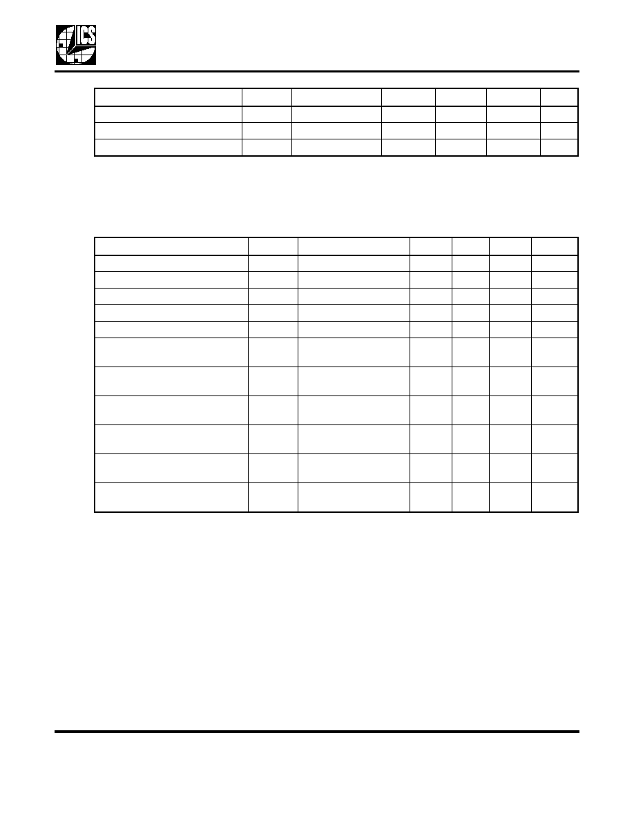
Pin Assignment
Multiplier Select Table
0 = connect directly to ground
1 = connect directly to VDD
Pin Descriptions
1
2
3
VDD
4
REFEN
5
6
GND
7
8
GND
REFOUT
S3
S1
GND
X2
S2
VDD
16
CLK
VDD
X1/ICLK
S0
OE
15
14
13
12
11
10
9
16 Pin (150 mil) TSSOP or SOIC
S3
S2
S1 S0
CLK (see note 2 on following page)
0
0
0
0
TEST
0
0
0
1
TEST
0
0
1
0
Input x1
0
0
1
1
Input x3
0
1
0
0
Input x4
0
1
0
1
Input x5
0
1
1
0
Input x6
0
1
1
1
Input x8
1
0
0
0
TEST
1
0
0
1
Crystal osc. pass through (no PLL)
1
0
1
0
Input x2
1
0
1
1
TEST
1
1
0
0
Input x8
1
1
0
1
Input x10
1
1
1
0
Input x12
1
1
1
1
Input x16
Pin
Number
Pin
Name
Pin
Type
Pin Description
1
CLK
Output
Clock output from VCO. Output frequency equals the input frequency times multiplier.
2
REFEN
Input
Reference clock enable. Turns off the buffered crystal oscillator clock (stops low) when low.
3
VDD
Power
Connect to +3.3V or +5V. Must match other VDDs.
4
VDD
Power
Connect to +3.3V or +5V. Must match other VDDs.
5
VDD
Power
Connect to +3.3V or +5V. Must match other VDDs.
6
X2
XO
Crystal connection. Connect to a 10 - 27 MHz fundamental parallel mode crystal.
Leave disconnected for an external clock input.
7
S1
Input
Multiplier select pin 1. Determines CLK output per table above. Internal pull-up.
8
X1/ICLK
XI
Crystal connection. Connect to a 10 - 27 MHz fundamental parallel mode crystal or clock.
9
S2
Input
Multiplier select pin 2. Determines CLK output per table above. Internal pull-up.
10
S3
Input
Multiplier select pin 3. Determines CLK output per table above. Internal pull-up.
11
S0
Input
Multiplier select pin 0. Determines CLK output per table above. Internal pull-up.
12
OE
Input
Output Enable. Tri-states both output clocks when low. Internal pull-up.
13
REFOUT
Output
Buffered crystal oscillator clock output. Controlled by REFIN.
14 - 16
GND
Power
Connect to ground.

L
OW
P
HASE
N
OISE
C
LOCK
M
ULTIPLIER
MDS 601-01 L
3
Revision 111204
I n t e gr a t e d C i r c u i t S y s t e m s
5 2 5 R a c e S t r e e t , S a n J o s e, C A 9 5 1 2 6
t e l ( 4 0 8 ) 2 9 7 - 1 2 0 1
w w w. i c s t . c o m
ICS601-01
Achieving Low Phase Noise
Figure 1 shows a typical phase noise measurement in a 125 MHz system. Therea are a few simple steps
that can be taken to achieve these levels of phase noise from the ICS601-01. Variations in VDD will
increase the hase noise, so it is important to have a stable, low noise supply voltage at the device. Use
decoupling capacitors of 0.1
µF in parallel with 0.01µF. It is important to have these capacitors as close as
possible to the ICS601-01 supply pins.
Disabling the REFOUT clock is also important for achieving low phase noise; lab tests have shown that this
can reduce the phase noise by as much as 10 dBc/Hz.
External Component/Crystal Selection
The ICS601-01 requires a minimum number of external components for proper operation. Decoupling
capacitors of 0.01
µF and 0.1µF should be connected between VDD and GND, as close to the part as
possible. A series termination resistor of 33
may be used for each clock output. The crystal must be
connected as close to the chip as possible. The crystal should be fundamental mode, parallel resonant. Do
not use third overtone. For exact tuning when using a crystal, capacitors should beconnected from pins X1
to ground and X2 to ground. In general, the value of these capacitors is given by the following equation,
where CL is the crystal load capacitance: Crystal caps (pF) = (CL - 5) x 2. So for a crystal with 16 pF load
capacitance, two 22 pF caps can be used. For any given board layout, ICS can measure the board
capacitance and recommend the exact capacitance value to use.
Figure 1. Phase Noise of ICS601-01 for 125 MHz output, 25 MHz crystal input.
VDD = 3.3 V, REFOUT disabled.
-140
-120
-100
-80
-60
-40
-20
0
1.00E+01
1.00E+02
1.00E+03
1.00E+04
1.00E+05
1.00E+06
1.00E+07
Offset from Carrier (Hz)
Phase Noise
(
dBc/Hz
)

L
OW
P
HASE
N
OISE
C
LOCK
M
ULTIPLIER
MDS 601-01 L
4
Revision 111204
I n t e gr a t e d C i r c u i t S y s t e m s
5 2 5 R a c e S t r e e t , S a n J o s e, C A 9 5 1 2 6
t e l ( 4 0 8 ) 2 9 7 - 1 2 0 1
w w w. i c s t . c o m
ICS601-01
Absolute Maximum Ratings
Stresses above the ratings listed below can cause permanent damage to the ICS601-01. These ratings,
which are standard values for ICS commercially rated parts, are stress ratings only. Functional operation of
the device at these or any other conditions above those indicated in the operational sections of the
specifications is not implied. Exposure to absolute maximum rating conditions for extended periods can
affect product reliability. Electrical parameters are guaranteed only over the recommended operating
temperature range.
Recommended Operation Conditions
DC Electrical Characteristics
VDD=3.3 V ±10%
, Ambient temperature -40 to +85
∞C
Item
Rating
Supply Voltage, VDD
7 V
All Inputs and Outputs
-0.5 V to VDD+0.5 V
Ambient Operating Temperature, Commercial version
0 to +70
∞C
Ambient Operating Temperature, Industrial version
-40 to +85
∞C
Storage Temperature
-65 to +150
∞C
Junction Temperature
125
∞C
Soldering Temperature
260
∞C
Parameter
Min.
Typ.
Max.
Units
Ambient Operating Temperature
-40
+85
∞C
Power Supply Voltage (measured in respect to GND)
+3.0
+5.5
V
Parameter
Symbol
Conditions
Min.
Typ.
Max.
Units
Operating Voltage
VDD
3.0
5.5
V
Input High Voltage
V
IH
X1/ICLK pin only
Note 1
VDD/2+1
V
Input Low Voltage
V
IL
X1/ICLK pin only
Note 1
VDD/2-1
V
Input High Voltage
V
IH
2
V
Input Low Voltage
V
IL
0.8
V
Output High Voltage
V
OH
CMOS level
I
OH
= -4mA
VDD-0.4
V
I
OH
= -12mA
2.4
Output Low Voltage
V
OL
I
OL
= 12mA
0.4
V
L
OW
P
HASE
N
OISE
C
LOCK
M
ULTIPLIER
MDS 601-01 L
5
Revision 111204
I n t e gr a t e d C i r c u i t S y s t e m s
5 2 5 R a c e S t r e e t , S a n J o s e, C A 9 5 1 2 6
t e l ( 4 0 8 ) 2 9 7 - 1 2 0 1
w w w. i c s t . c o m
ICS601-01
Note 1: Switching occurs nominally at VDD/2
AC Electrical Characteristics
VDD = 3.3V ±10%
, Ambient Temperature -40 to +85
∞ C
Note 2: Input frequency limited by maximum output frequency and multiplication factor (I.e. For 16x,
maximum input frequency is 13.75 MHz).
Operating Supply Current
IDD
No load, 125 MHz
22
30
mA
Short Circuit Current
Each output
±40
±60
mA
Input Capacitance
C
IN
OE, select pins
5
pF
Parameter
Symbol
Conditions
Min.
Typ.
Max.
Units
Input Frequency
Fin
10
27
MHz
Output Frequency
at 3.3V or 5V
156
MHz
Output Rise Time
t
OR
0.8 to 2.0V no load
1.5
ns
Output Fall Time
t
OF
0.8 to 2.0V, no load
1.5
ns
Output Clock Duty Cycle
at VDD/2
45
50
55
%
Maximum Absolute jitter, short
term, 125 MHz
No load
±50
±75
ps
Maximum jitter, one sigma,
125 MHz (x5)
No load
12
20
ps
Phase Noise, relative to carrier,
125 MHz (x5)
100 Hz offset
-90
-94
dBc/Hz
Phase Noise, relative to carrier,
125 MHz (x5)
1 kHz
-116
-120
dBc/Hz
Phase Noise, relative to carrier,
125 MHz (x5)
10 kHz offset
-118
-122
dBc/Hz
Phase Noise, relative to carrier,
125 MHz (x5)
100 kHz offset
-115
-119
dBc/Hz
Parameter
Symbol
Conditions
Min.
Typ.
Max.
Units

L
OW
P
HASE
N
OISE
C
LOCK
M
ULTIPLIER
MDS 601-01 L
6
Revision 111204
I n t e gr a t e d C i r c u i t S y s t e m s
5 2 5 R a c e S t r e e t , S a n J o s e, C A 9 5 1 2 6
t e l ( 4 0 8 ) 2 9 7 - 1 2 0 1
w w w. i c s t . c o m
ICS601-01
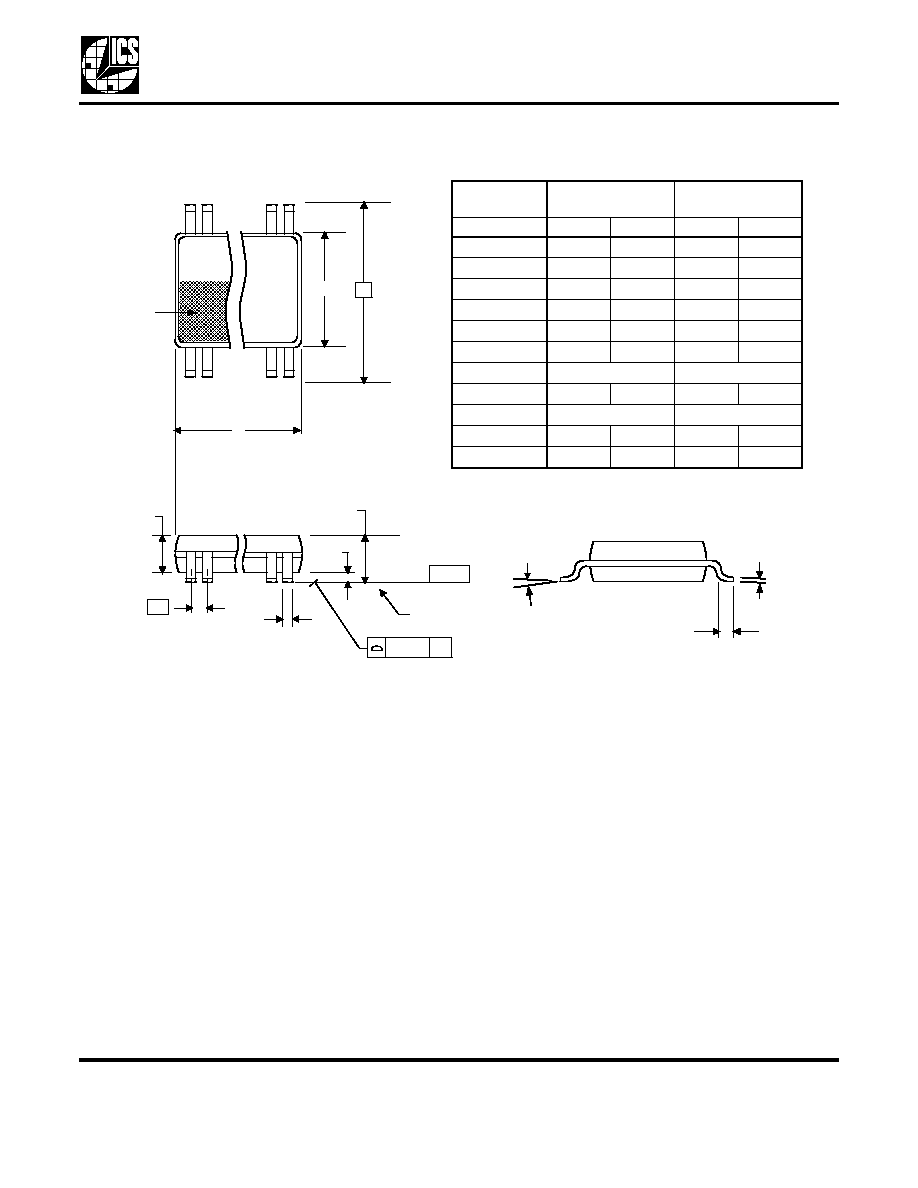
Package Outline and Package Dimensions
(16 pin SOIC, 150 Mil. Narrow Body)
Package dimensions are kept current with JEDEC Publication No. 95
I N D E X
A R E A
1 2
16
D
E
S E A T IN G
P LA N E
A 1
A
e
- C -
B
.1 0 (.0 0 4 )
C
C
L
H
SOIC
Symbol
Min
Max
A
1.35
1.75
A1
0.10
0.25
B
0.33
0.51
C
0.19
0.25
D
9.80
10.00
E
3.80
4.00
e
1.27 BASIC
H
5.80
6.20
L
0.40
1.27
0
∞
8
∞
L
OW
P
HASE
N
OISE
C
LOCK
M
ULTIPLIER
MDS 601-01 L
7
Revision 111204
I n t e gr a t e d C i r c u i t S y s t e m s
5 2 5 R a c e S t r e e t , S a n J o s e, C A 9 5 1 2 6
t e l ( 4 0 8 ) 2 9 7 - 1 2 0 1
w w w. i c s t . c o m
ICS601-01
Package Outline and Package Dimensions
(
16-pin TSSOP,
4.40 mm Body, 0.65 mm Pitch
)
Package dimensions are kept current with JEDEC Publication No. 95
INDEX
AREA
1 2
16
D
E1
E
SEATING
PLANE
A
1
A
A
2
e
- C -
b
.10 (.004)
C
c
L
Millimeters
Inches
Symbol
Min
Max
Min
Max
A
--
1.20
--
0.047
A1
0.05
0.15
0.002
0.006
A2
0.80
1.05
0.032
0.041
b
0.19
0.30
0.007
0.012
C
0.09
0.20
0.0035
0.008
D
4.90
5.1
0.193
0.201
E
6.40 BASIC
0.252 BASIC
E1
4.30
4.50
0.169
0.177
e
0.65 Basic
0.0256 Basic
L
0.45
0.75
0.018
0.030
0
∞
8
∞
0
∞
8
∞

L
OW
P
HASE
N
OISE
C
LOCK
M
ULTIPLIER
MDS 601-01 L
8
Revision 111204
I n t e gr a t e d C i r c u i t S y s t e m s
5 2 5 R a c e S t r e e t , S a n J o s e, C A 9 5 1 2 6
t e l ( 4 0 8 ) 2 9 7 - 1 2 0 1
w w w. i c s t . c o m
ICS601-01
Ordering Information
"L" designates Pb (lead) free package; "I" designates industrial grade.
While the information presented herein has been checked for both accuracy and reliability, Integrated Circuit Systems (ICS) assumes no
responsibility for either its use or for the infringement of any patents or other rights of third parties, which would result from its use. No other
circuits, patents, or licenses are implied. This product is intended for use in normal commercial applications. Any other applications such as those
requiring extended temperature range, high reliability, or other extraordinary environmental requirements are not recommended without
additional processing by ICS. ICS reserves the right to change any circuitry or specifications without notice. ICS does not authorize or warrant
any ICS product for use in life support devices or critical medical instruments.
Part / Order Number
Marking
Shipping Packaging
Package
Temperature
ICS601M-01
ICS601M-01
Tubes
16-pin narrow SOIC
0 to 70
∞ C
ICS601M-01T
ICS601M-01
Tape and Reel
16-pin narrow SOIC
0 to 70
∞ C
ICS601M-01I
ICS601M-01I
Tubes
16-pin narrow SOIC
-40 to 85
∞ C
ICS601M-01IT
ICS601M-01I
Tape and Reel
16-pin narrow SOIC
-40 to 85
∞ C
ICS601M-01LF
ICS601M-01LF
Tubes
16-pin narrow SOIC
0 to 70
∞ C
ICS601M-01LFT
ICS601M-01LF
Tape and Reel
16-pin narrow SOIC
0 to 70
∞ C
ICS601M-01ILF
ICS601M01ILF
Tubes
16-pin narrow SOIC
-40 to 85
∞ C
ICS601M-01ILFT
ICS601M01ILF
Tape and Reel
16-pin narrow SOIC
-40 to 85
∞ C
ICS601G-01
601G-01
Tubes
16-pin TSSOP
0 to 70
∞ C
ICS601G-01T
601G-01
Tape and Reel
16-pin TSSOP
0 to 70
∞ C
ICS601G-01I
601G-01I
Tubes
16-pin TSSOP
-40 to 85
∞ C
ICS601G-01IT
601G-01I
Tape and Reel
16-pin TSSOP
-40 to 85
∞ C
ICS601G-01LF
601G01LF
Tubes
16-pin TSSOP
0 to 70
∞ C
ICS601G-01LFT
601G01LF
Tape and Reel
16-pin TSSOP
0 to 70
∞ C
ICS601G-01ILF
601G01IL
Tubes
16-pin TSSOP
-40 to 85
∞ C
ICS601G-01ILFT
601G01IL
Tape and Reel
16-pin TSSOP
-40 to 85
∞ C