 | –≠–ª–µ–∫—Ç—Ä–æ–Ω–Ω—ã–π –∫–æ–º–ø–æ–Ω–µ–Ω—Ç: ICS604M | –°–∫–∞—á–∞—Ç—å:  PDF PDF  ZIP ZIP |

ICS604
Intel Graphics Clock Source
MDS 604 A
1
Revision 022499
Printed 11/14/00
Integrated Circuit Systems ∑ 525 Race Street ∑ San Jose ∑ CA ∑ 95126 ∑(408)295-9800tel∑(408)295-9818fax
PRELIMINARY
PRELIMINARY
INFORMATION
INFORMATION
∑ Packaged as 8 pin SOIC or die
∑ Compatible with Intel graphics controllers
∑ Zero ppm synthesis error on 48 MHz output
∑ Input frequency of 14.31818 MHz
∑ Output clock frequencies of 48 MHz,
24.576 MHz, plus 14.31818 MHz Reference
output
∑ Low jitter
∑ Operating voltages of 3.0 to 5.5 V
∑ Full CMOS-level outputs with 25 mA drive
capability at TTL levels
∑ Advanced, low power CMOS process
The ICS604 is the most cost effective way to
generate high quality, high frequency clocks for
Intel's latest generation of graphics controllers. It
provides 48 MHz for the graphics controller, a
24.576 MHz clock for video or audio, as well as a
14.31818 MHz buffered output for the system
clock. Using patented Phase-Locked-Loop (PLL)
techniques, the ICS604 requires only a standard
fundamental mode, inexpensive crystal.
ICS makes additional devices to meet multiple
graphic system requirements. If the 24.576 MHz
clock is not needed, use the ICS513. If additional
frequencies are required for different video
encoders and decoders, see the ICS614-01.
Block Diagram
Description
Features
14.318 MHz
48 MHz
24.576 MHz
Crystal
Oscillator
VDDC GND
PLL
Clock
Synthesis
and Control
Circuitry
14.318 MHz
crystal or clock
Output
Buffer
X1/ICLK
X2
Output
Buffer
Output
Buffer
VDDIO
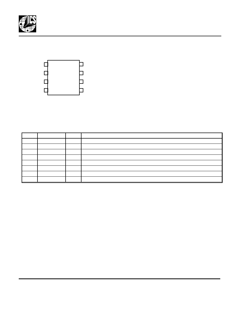
ICS604
Intel Graphics Clock Source
MDS 604 A
2
Revision 022499
Printed 11/14/00
Integrated Circuit Systems ∑ 525 Race Street ∑ San Jose ∑ CA ∑ 95126 ∑(408)295-9800tel∑(408)295-9818fax
PRELIMINARY
PRELIMINARY
INFORMATION
INFORMATION
Pin Assignment
Pin Descriptions
Key: I = Input; O = output; XI, XO = crystal connections; P = power supply connection
1
8
2
3
4
7
6
5
X1/ICLK
VDDC
GND
14.3M
X2
VDDIO
24.576M
48M
External Components / Crystal Selection
The ICS604 requires 0.01 µF decoupling capacitors to be connected between VDDC and GND, and
between VDDIO and GND. They must be connected close to the ICS604 to minimize lead inductance.
No external power supply filtering is required for this device. A 33
terminating resistor can be used next
to the output pins when driving 50
lines. The total on-chip crystal capacitance is approximately 6 pF,
and a parallel resonant, fundamental mode crystal should be used. Crystal capacitors should be connected
from each of the pins X1 and X2 to Ground as shown in the Block Diagram on page 1. The value (in pF)
of these crystal caps should be = (C
L
-6)*2, where C
L
is the crystal load capacitance in pF. For a clock
input, connect to X1 and leave X2 unconnected (no capacitors on either).
Number
Name
Type
Description
1
X1/ICLK
XI
Crystal connection for 14.31818 MHz crystal, or clock input.
2
VDDC
P
Connect to +3.3V or +5V. +5 V recommended for lowest output noise (jitter).
3
GND
P
Connect to ground.
4
14.3M
O
Buffered crystal oscillator output clock.
5
48M
O
48.0 MHz clock output for Intel graphics controller.
6
24.576M
O
24.576 MHz clock output.
7
VDDIO
P
Connect to +3.3 V or +5 V. Cannot be greater than VDDC.
8
X2
XO
Crystal connection for 14.31818 MHz crystal. Leave unconnected for clock input.

ICS604
Intel Graphics Clock Source
MDS 604 A
3
Revision 022499
Printed 11/14/00
Integrated Circuit Systems ∑ 525 Race Street ∑ San Jose ∑ CA ∑ 95126 ∑(408)295-9800tel∑(408)295-9818fax
PRELIMINARY
PRELIMINARY
INFORMATION
INFORMATION
Parameter
Conditions
Minimum
Typical
Maximum
Units
ABSOLUTE MAXIMUM RATINGS (note 1)
ABSOLUTE MAXIMUM RATINGS (note 1)
Supply Voltage, VDDC or VDDIO
Referenced to GND
7
V
Inputs
Referenced to GND
-0.5
VDDC+0.5
V
Clock Outputs
Referenced to GND
-0.5
VDDC+0.5
V
Ambient Operating Temperature
0
70
C
Soldering Temperature
Max of 10 seconds
260
C
Storage temperature
-65
150
C
DC CHARACTERISTICS (VDDC = 5 V unless otherwise noted)
DC CHARACTERISTICS (VDDC = 5 V unless otherwise noted)
Operating Voltage, VDDC
3
5.5
V
Operating Voltage, VDDIO
3
VDDC
V
Input High Voltage, VIH. Clock input
ICLK (Pin 1)
(VDDIO/2)+1 VDDIO/2
V
Input Low Voltage, VIL. Clock input
ICLK (Pin 1)
VDDIO/2
(VDDIO/2)-1
V
Output High Voltage, VOH
IOH=-8 mA
VDDIO-0.4
V
Output High Voltage, VOH
IOH=-25 mA
2.4
V
Output Low Voltage, VOL
IOL=25 mA
0.4
V
IDD Operating Supply Current
No load
18
mA
Short Circuit Current
Output clocks
100
mA
AC CHARACTERISTICS (VDDC = 5 V unless otherwise noted)
AC CHARACTERISTICS (VDDC = 5 V unless otherwise noted)
Input Frequency, crystal input
14.31818
MHz
Input Frequency, clock input
14.31818
MHz
Actual mean frequency error vs target
48.0 MHz
0
ppm
24.576 MHz
32
ppm
Output Clock Rise Time
0.8 to 2.0V
1
ns
Output Clock Fall Time
2.0 to 0.8V
1
ns
Output Clock Duty Cycle
at VDDIO/2
40
60
%
Absolute Clock Period Jitter, deviation
48.0 MHz
±250
ps
from mean. VDDC = 5 V, VDDIO = 3.3 V
24.576 MHz
±125
ps
Absolute Clock Period Jitter, deviation
48.0 MHz
±350
ps
from mean. VDDC = 3.3 V, VDDIO = 3.3 V 24.576 MHz
±160
ps
One Sigma Clock Period Jitter,
48.0 MHz
90
ps
VDDC = 5 V, VDDIO = 3.3 V
24.576 MHz
40
ps
One Sigma Clock Period Jitter,
48.0 MHz
110
ps
VDDC = 3.3 V, VDDIO = 3.3 V
24.576 MHz
50
ps
Electrical Specifications
Notes:
1. Stresses beyond those listed under Absolute Maximum Ratings could cause permanent damage to the device. Prolonged exposure
to levels above the operating limits but below the Absolute Maximums may affect device reliability.
2. Typical values are at 25 C.
ICS604
Intel Graphics Clock Source
MDS 604 A
4
Revision 022499
Printed 11/14/00
Integrated Circuit Systems ∑ 525 Race Street ∑ San Jose ∑ CA ∑ 95126 ∑(408)295-9800tel∑(408)295-9818fax
PRELIMINARY
PRELIMINARY
INFORMATION
INFORMATION
While the information presented herein has been checked for both accuracy and reliability, ICS assumes no responsibility for either its use or for the infringement of any patents or
other rights of third parties, which would result from its use. No other circuits, patents, or licenses are implied. This product is intended for use in normal commercial applications.
Any other applications such as those requiring extended temperature range, high reliability, or other extraordinary environmental requirements are not recommended without
additional processing by ICS. ICS reserves the right to change any circuitry or specifications without notice. ICS does not authorize or warrant any ICS product for use in life
support devices or critical medical instruments.
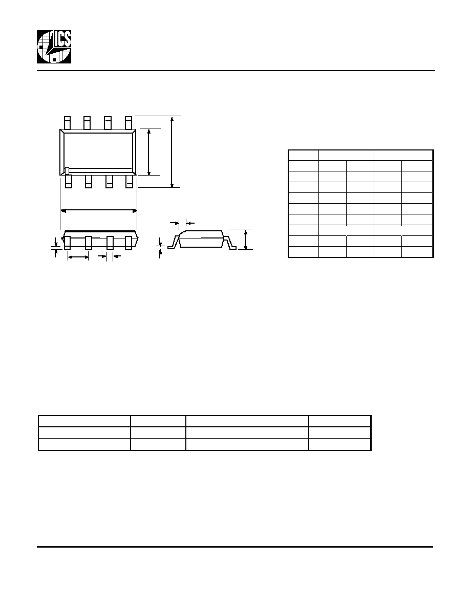
Package Outline and Package Dimensions
Inches
Inches
Millimeters
Millimeters
Symbol
Min
Max
Min
Max
A
0.055
0.068
1.397
1.7272
b
0.013
0.019
0.330
0.483
D
0.185
0.200
4.699
5.080
E
0.150
0.160
3.810
4.064
H
0.225
0.245
5.715
6.223
e .050 BSC
.050 BSC
1.27 BSC
1.27 BSC
h
0.015
0.381
Q
0.004
0.01
0.102
0.254
8 pin SOIC
Ordering Information
Part/Order Number
Marking
Package
Temperature
ICS604M
ICS604M
8 pin SOIC
0 - 70 C
ICS604MT
ICS604M
8 pin SOIC on tape and reel
0 - 70 C
c
A
b
D
E
H
e
h x 45∞
Q
Pin 1