 | –≠–ª–µ–∫—Ç—Ä–æ–Ω–Ω—ã–π –∫–æ–º–ø–æ–Ω–µ–Ω—Ç: ICS650-40 | –°–∫–∞—á–∞—Ç—å:  PDF PDF  ZIP ZIP |

ICS650-40
MDS 650-40 C
1
Revision 060705
I n t e gra t e d C i r c u i t S y s t e m s
5 2 5 R a c e S t r e e t , S a n J o s e, C A 9 5 1 2 6
t e l ( 4 0 8 ) 2 9 7 - 1 2 0 1
w w w. i c s t . c o m
E
THERNET
S
WITCH
C
LOCK
S
OURCE
Description
The ICS650-40 is a clock chip designed for use in
Ethernet Switch applications. Using ICS' patented
Phase-Locked Loop (PLL) techniques, the device takes
a 25 MHz crystal input and produces various output
clock frequencies as listed in Output Select Table.
Features
∑
Packaged in 16-pin TSSOP
∑
Available in Pb (lead) free package
∑
Operating voltage of 3.3 V
∑
Low power consumption
∑
Input frequency of 25 MHz
∑
Low long-term jitter
∑
2.5 V to 3.3 V clock outputs
Block Diagram
Phase Lock Loop
Clock
Buffer/
Crystal
Oscillator
VDD
GND
3
4
X1/ICLK
X2
25 MHz
crystal or clock
Control
Logic
OE
S1:S0
CLKB
2
CLKA
Optional tuning crystal
capacitors
VDDOA
VDDOB
E
THERNET
S
WITCH
C
LOCK
S
OURCE
MDS 650-40 C
2
Revision 060705
I n t e gr a t e d C i r c u i t S y s t e m s
5 2 5 R a c e S t r e e t , S a n J o s e, C A 9 5 1 2 6
t e l ( 4 0 8 ) 2 9 7 - 1 2 0 1
w w w. i c s t . c o m
ICS650-40
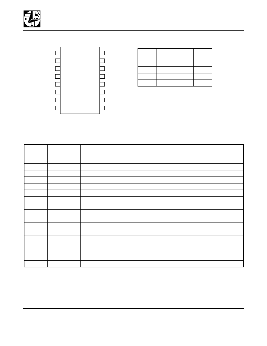
Pin Assignment
Output Select Table (MHz)
Pin Descriptions
1
2
3
X2
4
VDD
5
6
7
8
VDDOA
S1
OE
GND
16
X1/ICLK
GND
15
14
13
12
11
10
9
16-pin (173 mil) TSSOP
CLKB
CLKA
VDDOB
GND
S0
GND
VDD
VDD
S1
S0
CLKA
(MHz)
CLKB
(MHz)
0
0
127
127
0
1
133
133
1
0
157
157
1
1
189
189
Pin
Number
Pin
Name
Pin
Type
Pin Description
1
X1/ICLK
Input
Crystal or clock input. Connect to a 25 MHz crystal or single ended clock.
2
VDD
Power
Connect to +3.3 V.
3
GND
Power
Connect to ground.
4
VDDOA
Power
Connect to +2.5 V or +3.3 V. For clock output buffer A only.
5
CLKA
Output
Clock A output with weak pull-down resistor.
6
CLKB
Output
Clock B output with weak pull-down resistor.
7
VDDOB
Power
Connect to +2.5 V or +3.3 V. For clock output buffer B only.
8
GND
Power
Connect to ground.
9
S0
Input
Select pin 0.
10
S1
Input
Select pin 1.
11
VDD
Power
Connect to +3.3 V.
12
VDD
Power
Connect to +3.3 V.
13
GND
Power
Connect to ground.
14
OE
Input
Output enable tri-states outputs and device is not shut down. Internal
pull-up resistor.
15
GND
Power
Connect to ground.
16
X2
Output
Crystal connection. Leave unconnected for clock input.

E
THERNET
S
WITCH
C
LOCK
S
OURCE
MDS 650-40 C
3
Revision 060705
I n t e gr a t e d C i r c u i t S y s t e m s
5 2 5 R a c e S t r e e t , S a n J o s e, C A 9 5 1 2 6
t e l ( 4 0 8 ) 2 9 7 - 1 2 0 1
w w w. i c s t . c o m
ICS650-40
External Components
A minimum number of external components are required for proper operation. Decoupling capacitors of
0.01
µF should be connected between VDD and GND pairs. The capacitors should be placed between pins
VDD and GND, and VDDO and GND, as close to the device as possible. A 33
series terminating resistor
should be used on each clock output if the trace is longer than 1 inch. A 25 MHz fundamental mode parallel
resonant crystal should be used with C
L
=18 pF.
On chip capacitors. On Chip capacitors are used for a 18 pF load crystal. Small 2 to 3 pf trimming
capacitors are used from pins X1 to ground and X2 to ground to optimize the initial accuracy.
Absolute Maximum Ratings
Stresses above the ratings listed below can cause permanent damage to the ICS650-40. These ratings,
which are standard values for ICS commercially rated parts, are stress ratings only. Functional operation of
the device at these or any other conditions above those indicated in the operational sections of the
specifications is not implied. Exposure to absolute maximum rating conditions for extended periods can
affect product reliability. Electrical parameters are guaranteed only over the recommended operating
temperature range.
Recommended Operation Conditions
Item
Rating
Supply Voltage, VDD
7 V
All Inputs and Outputs
-0.5 V to VDD+0.5 V
Ambient Operating Temperature
0 to +70
∞C
Storage Temperature
-65 to +150
∞C
Junction Temperature
125
∞C
Soldering Temperature
260
∞C
Parameter
Min.
Typ.
Max.
Units
Ambient Operating Temperature
0
+70
∞C
Power Supply Voltage (measured in respect to GND)
+3.15
+3.45
V

E
THERNET
S
WITCH
C
LOCK
S
OURCE
MDS 650-40 C
4
Revision 060705
I n t e gr a t e d C i r c u i t S y s t e m s
5 2 5 R a c e S t r e e t , S a n J o s e, C A 9 5 1 2 6
t e l ( 4 0 8 ) 2 9 7 - 1 2 0 1
w w w. i c s t . c o m
ICS650-40
DC Electrical Characteristics
Unless otherwise specified, VDD=3.3 V ±5%, Ambient Temperature 0 to +70
∞C
Note: 1. Nominal switching threshold is VDD/2.
AC Electrical Characteristics
, VDD = 3.3 V ±5%, VDDO = 2.5 - 3.3 V ±5%, C
L
=10 pF Ambient Temperature 0 to +70
∞ C
Parameter
Symbol
Conditions
Min.
Typ.
Max.
Units
Operating Voltage
VDD
3.15
3.45
V
Output Operating Voltage
VDDOA,B
2.375
3.45
V
Input High Voltage, ICLK
V
IH
Note 1
VDD/2+0.5
V
Input Low Voltage, ICLK
V
IL
Note 1
VDD/2-0.5
V
Input High Voltage, S1:S0:OE
V
IH
2
VDD
V
Input Low Voltage, S1:S0:OE
V
IL
0.4
V
Output High Voltage
V
OH
I
OH
= -12 mA
2
V
Output Low Voltage
V
OL
I
OL
= 12 mA
0.4
V
Operating Supply Current
IDD
No load
40
mA
IDD at Output Disable
Condition(OE low)
No load
16
mA
Short Circuit Current
I
OS
Each output
±35
mA
Internal Pull-up Resistor
R
PUP
OE pin
250
k
Internal Pull-down Resistor
R
PD
CLK outputs
525
k
Parameter
Symbol
Conditions
Min.
Typ.
Max.
Units
Input Frequency
25
MHz
Output Rise Time
t
OR
20% to 80% of VDD
1.6
ns
Output Fall Time
t
OF
80% to 20% of VDD
1.6
ns
Output Clock Duty Cycle
at VDD/2
40
49-51
60
%
Frequency Error
all clocks
0
ppm
Output to Output Skew
between clocks of the same
frequency
250
ps
Absolute Jitter, Short-term P-P
variation from mean
±100
±200
ps
Absolute Jitter, Short-term C-C
200
400
ps
Long-term Jitter
1000 clock cycles
250
400
ps

E
THERNET
S
WITCH
C
LOCK
S
OURCE
MDS 650-40 C
5
Revision 060705
I n t e gr a t e d C i r c u i t S y s t e m s
5 2 5 R a c e S t r e e t , S a n J o s e, C A 9 5 1 2 6
t e l ( 4 0 8 ) 2 9 7 - 1 2 0 1
w w w. i c s t . c o m
ICS650-40
Thermal Characteristics
(16-pin TSSOP)
Marking Diagram
Marking Diagram
Notes:
1. ###### is the lot code.
2. YYWW is the last two digits of the year, and the week number that the part was assembled.
3. "LF" designates Pb (lead ) free package.
4. Bottom marking: (origin). Origin = country of origin if not USA.
Parameter
Symbol
Conditions
Min.
Typ.
Max.
Units
Thermal Resistance Junction to
Ambient
JA
Still air
78
∞C/W
JA
1 m/s air flow
70
∞C/W
JA
3 m/s air flow
68
∞C/W
Thermal Resistance Junction to Case
JC
37
∞C/W
8
16
9
650G-40
######
YYWW
ICS
1
8
16
9
650G40LF
######
YYWW
ICS
1
E
THERNET
S
WITCH
C
LOCK
S
OURCE
MDS 650-40 C
6
Revision 060705
I n t e gr a t e d C i r c u i t S y s t e m s
5 2 5 R a c e S t r e e t , S a n J o s e, C A 9 5 1 2 6
t e l ( 4 0 8 ) 2 9 7 - 1 2 0 1
w w w. i c s t . c o m
ICS650-40
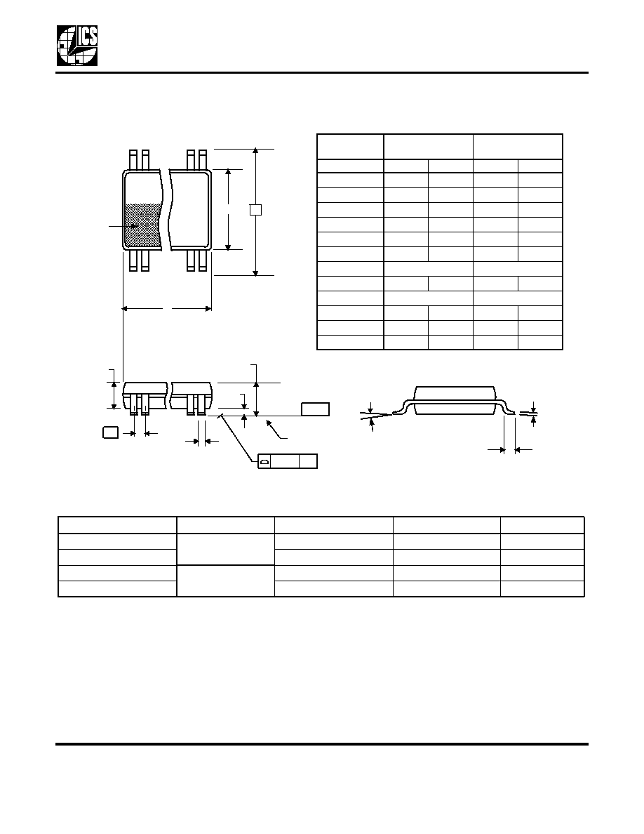
Package Outline and Package Dimensions
(16-pin TSSOP, 173 Mil. Narrow Body)
Package dimensions are kept current with JEDEC Publication No. 95
Ordering Information
Parts that are ordered with a "LF" suffix to the part number are the Pb-Free configuration and are RoHS compliant.
While the information presented herein has been checked for both accuracy and reliability, Integrated Circuit Systems (ICS)
assumes no responsibility for either its use or for the infringement of any patents or other rights of third parties, which would
result from its use. No other circuits, patents, or licenses are implied. This product is intended for use in normal commercial
applications. Any other applications such as those requiring extended temperature range, high reliability, or other extraordinary
environmental requirements are not recommended without additional processing by ICS. ICS reserves the right to change any
circuitry or specifications without notice. ICS does not authorize or warrant any ICS product for use in life support devices or
critical medical instruments.
Part / Order Number
Marking
Shipping Packaging
Package
Temperature
ICS650G-40
See Page 6
Tubes
16-pin TSSOP
0 to +70
∞ C
ICS650G-40T
Tape and Reel
16-pin TSSOP
0 to +70
∞ C
ICS650G-40LF
See Page 6
Tubes
16-pin TSSOP
0 to +70
∞ C
ICS650G-40LFT
Tape and Reel
16-pin TSSOP
0 to +70
∞ C
D
E
H
b
e
a
Pin 1
Index
Area
c
A
L
IN D E X
A R E A
1 2
16
D
E 1
E
S E A T IN G
P LA N E
A
1
A
A
2
e
- C -
b
aaa
C
c
L
Millimeters
Inches
Symbol
Min
Max
Min
Max
A
--
1.20
--
0.047
A1
0.05
0.15
0.002
0.006
A2
0.80
1.05
0.032
0.041
b
0.19
0.30
0.007
0.012
C
0.09
0.20
0.0035
0.008
D
4.90
5.1
0.193
0.201
E
6.40 BASIC
0.252 BASIC
E1
4.30
4.50
0.169
0.177
e
0.65 Basic
0.0256 Basic
L
0.45
0.75
0.018
0.030
0
∞
8
∞
0
∞
8
∞
aaa
--
0.10
--
0.004