ICS650-36
MDS 650-36 D
1
Revision 030206
I n t e gra t e d C i r c u i t S y s t e m s
5 2 5 R a c e S t r e e t , S a n J o s e, C A 9 5 1 2 6
t e l ( 4 0 8 ) 2 9 7 - 1 2 0 1
w w w. i c s t . c o m
Networking & PCI Clock Source
Description
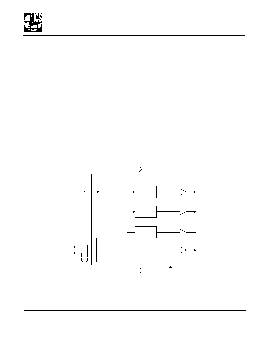
The ICS650-36 is a low cost frequency generator
designed to support networking and PCI applications.
Using analog/digital Phase Locked-Loop (PLL)
techniques, the device uses a standard fundamental
mode, inexpensive crystal input of 25 MHz to produce
four output clocks supporting LAN, PCI, and 100M
SDRAM functions.
The device also has a power down feature that
tri-states the clock outputs and turns off the PLL when
the PDTS pin is taken low.
Features
∑
Packaged in 16-pin TSSOP
∑
Available in Pb (lead) free package
∑
Replaces multiple crystals and oscillators
∑
Input crystal or clock frequency of 25 MHz
∑
Fixed reference output frequency of 25 MHz
∑
Selectable output frequencies of 33.3, 33.333, 50,
66.666, 100, and 125 MHz
∑
Duty cycle of 40/60
∑
Operating voltage of 3.3 V
∑
Advanced, low-power CMOS process
∑
Industrial and commercial temperature ranges
Block Diagram
X1/ICLK
X2
PLL1
PLL2
Crystal
Oscillator/
Clock
Buffer
25 MHz
crystal
input
External capacitors
may be required.
VDD
GND
PDTS
(all outputs and PLLs)
CLK1
3
3
PLL3
CLK3
CLK2
REF
Select/
Control
Circuit
3
S2:0

Networking & PCI Clock Source
MDS 650-36 D
2
Revision 030206
I n t e gr a t e d C i r c u i t S y s t e m s
525 Race Street, San Jose, CA 95126
tel (408) 297-1201
www.icst.com
ICS650-36
Pin Assignment
CLK Output Selection Table
Note: All frequencies are in MHz.
Pin Descriptions
12
1
11
2
10
3
9
X2
4
X1
5
GND
6
GND
7
CLK3
8
PDTS
REF
S0
VDD
S2
CLK1
S1
CLK2
GND
16
15
14
13
VDD
VDD
16-pin (173 mil) TSSOP
S2
S1
S0
REF
CLK1
CLK2
CLK3
0
0
0
OFF
33.30
50
125
0
0
1
ON
33.333
33.333
125
0
1
0
ON
33.333
66.666
125
0
1
1
ON
66.666
66.666
125
1
0
0
ON
33.333
50
125
1
0
1
ON
33.333
50
100
1
1
0
ON
33.333
66.666
100
1
1
1
ON
33.30
50
125
Pin
Number
Pin
Name
Pin
Type
Pin Description
1
X2
Output
Crystal connection. Connect to 25 MHz crystal input or float for
clock.
2
X1
Input
Crystal connection. Connect to 25 MHz crystal or clock input.
3
GND
Power
Connect to ground.
4
CLK3
Output
Selectable clock output. See table above for frequency. Weak
internal pull-down when tri-state.
5
PDTS
Input
Powers down entire chip and tri-states outputs when low. Internal
pull-up resistor.
6
S2
Input
Select pin. Selects clock output frequency from table above.
Internal pull-up resistor.
7
CLK2
Output
Selectable clock output. See table above for frequency. Weak
internal pull-down when tri-state.
8
VDD
Power
Connect to +3.3 V.
9
S1
Input
Select pin. Selects clock output frequency from table above.
Internal pull-up resistor.
10
GND
Power
Connect to ground.
11
CLK1
Output
Selectable clock output. See table above for frequency. Weak
internal pull-down when tri-state.
12
VDD
Power
Connect to +3.3 V.
13
S0
Input
Select pin. Selects clock output frequency from table above.
Internal pull-up resistor.
Networking & PCI Clock Source
MDS 650-36 D
3
Revision 030206
I n t e gr a t e d C i r c u i t S y s t e m s
525 Race Street, San Jose, CA 95126
tel (408) 297-1201
www.icst.com
ICS650-36
External Components
Decoupling Capacitor
As with any high performance mixed-signal IC, the
ICS650-36 must be isolated from system power supply
noise to perform optimally.
A decoupling capacitor of 0.01µF must be connected
between each VDD and the PCB ground plane.
Series Termination Resistor
Clock output traces over one inch should use series
termination. To series terminate a 50
trace (a
commonly used trace impedance), place a 33
resistor
in series with the clock line, as close to the clock output
pin as possible. The nominal impedance of the clock
output is 20
.
Crystal Load Capacitors
The device crystal connections should include pads for
small capacitors from X1 to ground and from X2 to
ground. These capacitors are used to adjust the stray
capacitance of the board to match the nominally
required crystal load capacitance. Because load
capacitance can only be increased in this trimming
process, it is important to keep stray capacitance to a
minimum by using very short PCB traces (and no vias)
between the crystal and device. Crystal capacitors
must be connected from each of the pins X1 and X2 to
ground.
The value (in pF) of these crystal caps should equal
(C
L
-6 pF)*2. In this equation, C
L
= crystal load
capacitance in pF. Example: For a crystal with a 16 pF
load capacitance, each crystal capacitor would be 20
pF [(16-6) x 2 = 20].
PCB Layout Recommendations
Observed the following guidelines for optimum device
performance and lowest output phase noise:
1) The 0.01µF decoupling capacitors should be
mounted on the component side of the board as close
to the VDD pin as possible. No vias should be used
between the decoupling capacitors and VDD pins. The
PCB trace to VDD pins should be kept as short as
possible, as should the PCB trace to the ground via.
2) The external crystal should be mounted just next to
the device with short traces. The X1 and X2 traces
should not be routed next to each other with minimum
spaces, instead they should be separated and away
from other traces.
3) Place the 33
series termination resistor (if needed)
close to the clock output to minimize EMI.
4) An optimum layout is one with all components on the
same side of the board, minimizing vias through other
signal layers. Other signal traces should be routed
away from the ICS650-36. This includes signal traces
just underneath the device, or on layers adjacent to the
ground plane layer used by the device.
14
REF
Output
Reference 25 MHz clock output. Weak internal pull-down when
tri-state.
15
GND
Power
Connect to ground.
16
VDD
Power
Connect to +3.3 V.
Pin
Number
Pin
Name
Pin
Type
Pin Description
Networking & PCI Clock Source
MDS 650-36 D
4
Revision 030206
I n t e gr a t e d C i r c u i t S y s t e m s
525 Race Street, San Jose, CA 95126
tel (408) 297-1201
www.icst.com
ICS650-36
Absolute Maximum Ratings
Stresses above the ratings listed below can cause permanent damage to the ICS650-36. These ratings,
which are standard values for ICS commercially rated parts, are stress ratings only. Functional operation of
the device at these or any other conditions above those indicated in the operational sections of the
specifications is not implied. Exposure to absolute maximum rating conditions for extended periods can
affect product reliability. Electrical parameters are guaranteed only over the recommended operating
temperature range.
Recommended Operation Conditions
Item
Rating
Supply Voltage, VDD
-0.5 V to 7 V
All Inputs and Outputs
-0.5 V to VDD+0.5 V
Ambient Operating Temperature (commercial)
0 to +70
∞C
Ambient Operating Temperature (industrial)
-40 to +85
∞C
Storage Temperature
-65 to +150
∞C
Junction Temperature
125
∞C
Soldering Temperature
260
∞C
Parameter
Min.
Typ.
Max.
Units
Ambient Operating Temperature (commercial)
0
+70
∞C
Ambient Operating Temperature (industrial)
-40
+85
∞C
Power Supply Voltage (measured in respect to GND)
+3.135
+3.3
+3.465
V

Networking & PCI Clock Source
MDS 650-36 D
5
Revision 030206
I n t e gr a t e d C i r c u i t S y s t e m s
525 Race Street, San Jose, CA 95126
tel (408) 297-1201
www.icst.com
ICS650-36
DC Electrical Characteristics
Unless stated otherwise, VDD = 3.3 V ±5%, Ambient Temperature -40 to +85
∞C
AC Electrical Characteristics
Unless stated otherwise, VDD = 3.3 V ±5%, Ambient Temperature -40 to +85
∞C
Note 1: Measured with a 15 pF load.
Parameter
Symbol
Conditions
Min.
Typ.
Max.
Units
Operating Voltage
VDD
3.135
3.3
3.465
V
Supply Current
IDD
No load, PDTS=1
25
mA
Power Down Current
IDDPD
No load, PDTS=0
100
µA
Input High Voltage
V
IH
PDTS, S2:0
2
V
Input Low Voltage
V
IL
PDTS, S2:0
0.8
V
Output High Voltage
V
OH
I
OH
= -4 mA
VDD-0.3
V
Output High Voltage
V
OH
I
OH
= -12 mA
2.4
V
Output Low Voltage
V
OL
I
OL
= 12 mA
0.4
V
Short Circuit Current
I
OS
Clock outputs
±65
mA
Input Capacitance, inputs
C
IN
5
pF
Nominal Output Impedance
Z
OUT
20
Internal Pull-up Resistor
R
PU
PDTS, S2:0
500
k
Internal Pull-down Resistor
R
PD
Outputs
250
k
Parameter
Symbol
Conditions
Min.
Typ.
Max.
Units
Input Frequency
f
IN
25
MHz
Output Rise Time
t
OR
20% to 80%, Note 1
0.8
ns
Output Fall Time
t
OF
80% to 20%, Note 1
0.7
ns
Output Clock Duty Cycle
at VDD/2, Note 1
40
60
%
Absolute Clock Period Jitter
Note 1
±125
ps
Clock Jitter, Cycle-to-Cycle
33.333M, 66.666M,
Note 1
150
ps
Clock Jitter, Long Term
25M, n=1000, Note1
900
ps
Frequency Synthesis Error
0
ppm
Output Enable Time
t
OE
PDTS high to output
locked to ±1%
350
µs
Output Disable Time
t
OD
PDTS low to tri-state
25
ns
Networking & PCI Clock Source
MDS 650-36 D
6
Revision 030206
I n t e gr a t e d C i r c u i t S y s t e m s
525 Race Street, San Jose, CA 95126
tel (408) 297-1201
www.icst.com
ICS650-36
Thermal Characteristics
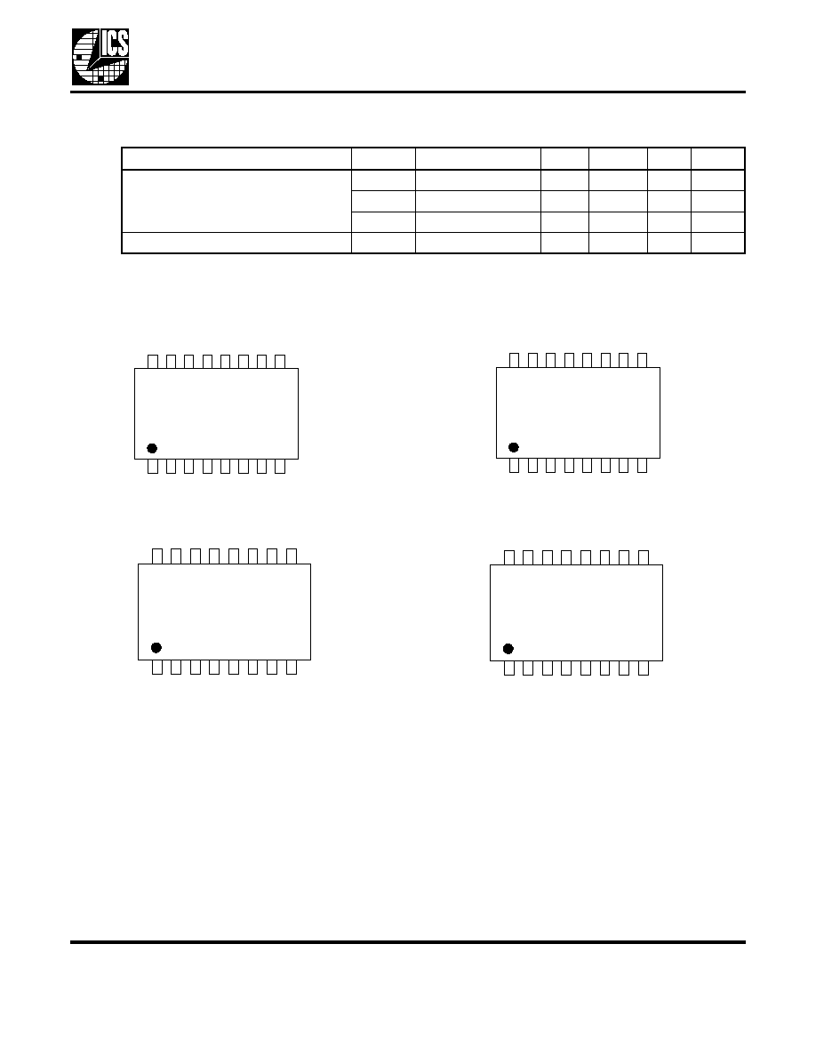
Marking Diagrams
(ICS650G-36)
(ICS650GI-36)
(ICS650G-36LF)
(ICS650GI-36LF)
Notes:
1. ###### is the lot code.
2. YYWW is the last two digits of the year, and the week number that the part was assembled.
3. "LF" or "L" designates Pb free packaging.
4. "I" designates industrial temperature range.
5. Bottom marking: (origin). Origin = country of origin if not USA.
Parameter
Symbol
Conditions
Min.
Typ.
Max.
Units
Thermal Resistance Junction to
Ambient
JA
Still air
78
∞C/W
JA
1 m/s air flow
70
∞C/W
JA
3 m/s air flow
68
∞C/W
Thermal Resistance Junction to Case
JC
37
∞C/W
1
8
9
16
650G-36
######
YYWW$$
1
8
9
16
650GI-36
######
YYWW$$
1
8
9
16
650G36LF
######
YYWW
1
8
9
16
650GI36L
######
YYWW
Networking & PCI Clock Source
MDS 650-36 D
7
Revision 030206
I n t e gr a t e d C i r c u i t S y s t e m s
525 Race Street, San Jose, CA 95126
tel (408) 297-1201
www.icst.com
ICS650-36
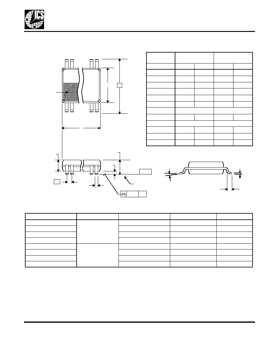
Package Outline and Package Dimensions
(16-pin TSSOP, 173 Mil. Narrow Body)
Package dimensions are kept current with JEDEC Publication No. 95
Ordering Information
Parts that are ordered with a "LF" suffix to the part number are the Pb-Free configuration and are RoHS compliant.
While the information presented herein has been checked for both accuracy and reliability, Integrated Circuit Systems (ICS)
assumes no responsibility for either its use or for the infringement of any patents or other rights of third parties, which would
result from its use. No other circuits, patents, or licenses are implied. This product is intended for use in normal commercial
applications. Any other applications such as those requiring extended temperature range, high reliability, or other extraordinary
environmental requirements are not recommended without additional processing by ICS. ICS reserves the right to change any
circuitry or specifications without notice. ICS does not authorize or warrant any ICS product for use in life support devices or
critical medical instruments.
Part / Order Number
Marking
Shipping Packaging
Package
Temperature
ICS650G-36
(see page 6)
Tubes
16-pin TSSOP
0 to +70
∞C
ICS650G-36T
Tape and Reel
16-pin TSSOP
0 to +70
∞C
ICS650G-36LF
Tubes
16-pin TSSOP
0 to +70
∞C
ICS650G-36LFT
Tape and Reel
16-pin TSSOP
0 to +70
∞C
ICS650GI-36
(see page 6)
Tubes
16-pin TSSOP
-40 to +85
∞C
ICS650GI-36T
Tape and Reel
16-pin TSSOP
-40 to +85
∞C
ICS650GI-36LF
Tubes
16-pin TSSOP
-40 to +85
∞C
ICS650GI-36LFT
Tape and Reel
16-pin TSSOP
-40 to +85
∞C
IN D E X
A R E A
1 2
16
D
E 1
E
S E A T IN G
P LA N E
A
1
A
A
2
e
- C -
b
aaa
C
c
L
*For reference only. Controlling dimensions in mm.
Millimeters
Inches*
Symbol
Min
Max
Min
Max
A
--
1.20
--
0.047
A1
0.05
0.15
0.002
0.006
A2
0.80
1.05
0.032
0.041
b
0.19
0.30
0.007
0.012
C
0.09
0.20
0.0035
0.008
D
4.90
5.1
0.193
0.201
E
6.40 BASIC
0.252 BASIC
E1
4.30
4.50
0.169
0.177
e
0.65 Basic
0.0256 Basic
L
0.45
0.75
0.018
0.030
0
∞
8
∞
0
∞
8
∞
aaa
--
0.10
--
0.004