ICS650-05
HDTV Clock Synthesizer
MDS 650-05 A
1
Revision 081199 Printed 12/4/00
Integrated Circuit Systems ∑ 525 Race Street ∑ San Jose ∑CA∑95126∑ (408) 295-9800tel ∑ (408) 295-9818fax
PRELIMINARY
PRELIMINARY
INFORMATION
INFORMATION
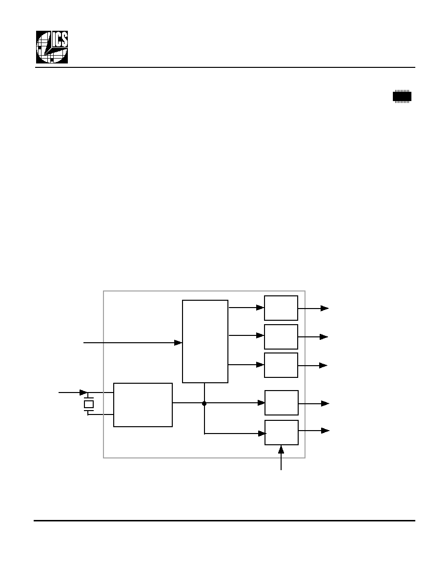
The ICS650-05 is a low cost, low jitter, high
performance clock synthesizer designed to
produce 74.175824 MHz and 74.250000 MHz as
necessary for HDTV applications. Using our
patented analog Phase-Locked Loop (PLL)
techniques, the device uses a 27.0 MHz clock or
fundamental crystal input to produce buffered,
fixed clocks and a selectable frame rate clock for
HDTV systems.
Block Diagram
Description
Features
∑ Packaged in 20 pin tiny SSOP (QSOP)
∑ Input Frequency of 27.0 MHz
∑ Zero ppm synthesis error in output clocks
∑ Provides fixed 13.5 MHz, dual 27.0 MHz, and
54.0 MHz output clocks with a selectable Frame
Rate Clock of 74.175824 MHz or
74.250000 MHz
∑ Ideal for HDTV applications
∑ 3.3 V or 5.0 V operating voltage
27.0 MHz
Input
Buffer/Crystal
Oscillator
Clock
Synthesis
and
Control
Circuit
Output
Buffer
Output
Buffers
Output
Buffer
27.0 MHz
Output
Buffer
Output
Buffers
FRS
27.0 MHz
FRCLK
54.0 MHz
13.5 MHz
OE (all outputs)
ICS650-05
HDTV Clock Synthesizer
MDS 650-05 A
2
Revision 081199 Printed 12/4/00
Integrated Circuit Systems ∑ 525 Race Street ∑ San Jose ∑CA∑95126∑ (408) 295-9800tel ∑ (408) 295-9818fax
PRELIMINARY
PRELIMINARY
INFORMATION
INFORMATION
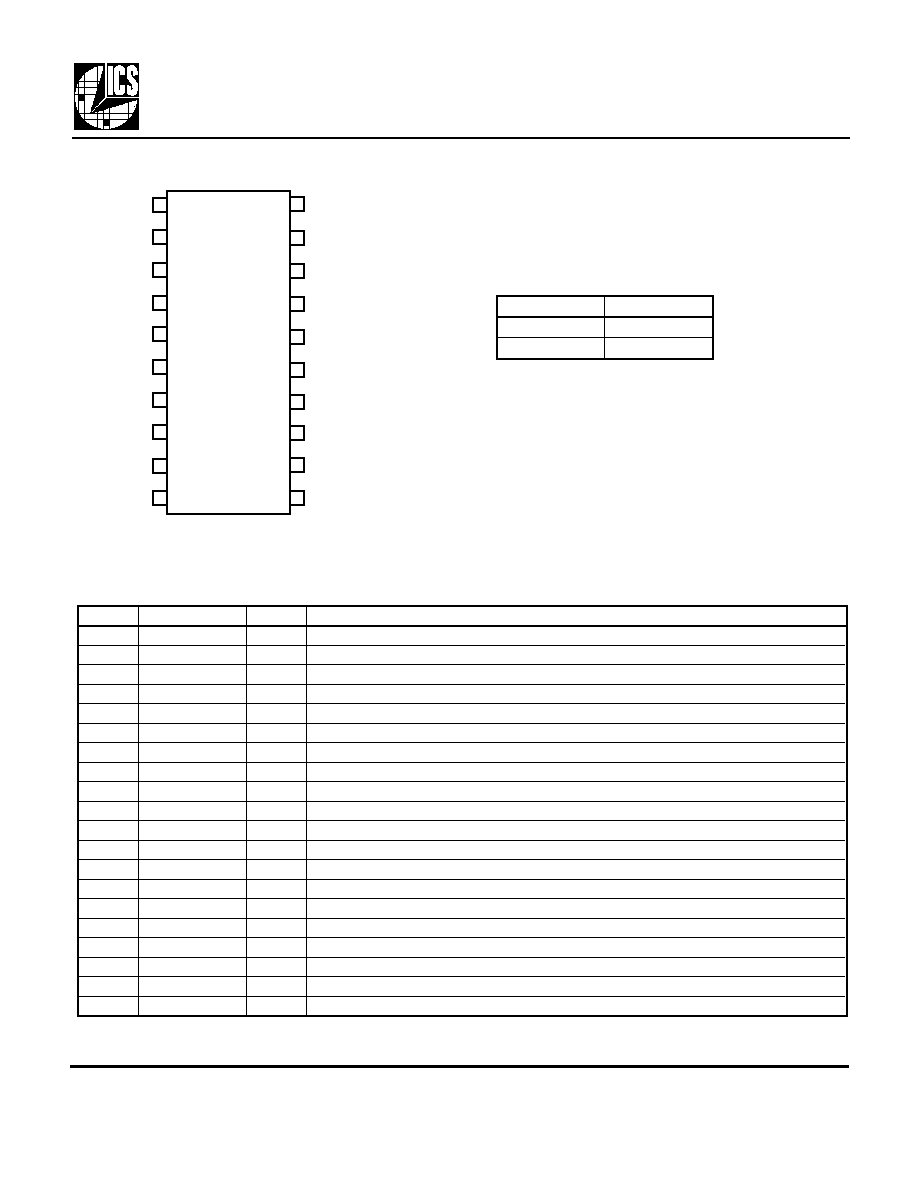
Pin #
Name
Type
Description
1
VDD
P
Connect to +3.3 V or +5.0 V. Must be same as other VDDs.
2
X2
XO
Crystal connection to a 27.0 MHz crystal or leave unconnected for clock input
3
X1/ICLK
XI
Crystal connection. Connect to a 27.0 MHz fundamental mode crystal or clock input.
4
VDD
P
Connect to +3.3 V or +5.0 V. Must be same as other VDDs.
5
VDD
P
Connect to +3.3 V or +5.0 V. Must be same as other VDDs.
6
GND
P
Connect to ground.
7
NC
-
No Connect. Do not connect anything to this pin.
8
27M
O
27 MHz buffered oscillator clock output.
9
13.5M
O
13.5 MHz clock output.
10
GND
P
Connect to ground.
11
GND
P
Connect to ground.
12
27M
O
27 MHz buffered clock output.
13
54M
O
54 MHz buffered clock output.
14
GND
P
Connect to ground.
15
GND
P
Connect to ground.
16
VDD
P
Connect to +3.3 V or +5.0 V. Must be same as other VDDs.
17
FRCLK
O
Frame Rate Clock as shown on table.
18
FRS
I
Frame Rate Frequency Select input pin. Determines FRCLK output as shown on table.
19
OE
I
Output Enable. Tri-states all clocks when low.
20
VDD
P
Connect to +3.3 V or +5.0 V. Must be same as other VDDs.
Pin Descriptions
Key: I = Input with internal pull-up; O = output; P = power supply connection; XI, XO = crystal
connections
1
16
2
3
4
15
14
13
VDD
NC
X2
VDD
20 pin SSOP (QSOP)
5
6
7
8
12
11
10
9
GND
OE
X1/ICLK
VDD
FRS
VDD
FRCLK
27M
GND
13.5M
27M
18
17
19
20
GND
VDD
54M
GND
GND
Pin Assignment
FRCLK Output Select Table (in MHz)
FRS Pin 18
FRCLK Pin 17
0
74.175824
1
74.250000

ICS650-05
HDTV Clock Synthesizer
MDS 650-05 A
3
Revision 081199 Printed 12/4/00
Integrated Circuit Systems ∑ 525 Race Street ∑ San Jose ∑CA∑95126∑ (408) 295-9800tel ∑ (408) 295-9818fax
PRELIMINARY
PRELIMINARY
INFORMATION
INFORMATION
Parameter
Conditions
Minimum
Typical
Maximum
Units
ABSOLUTE MAXIMUM RATINGS (note 1)
ABSOLUTE MAXIMUM RATINGS (note 1)
Supply voltage, VDD
Referenced to GND
7
V
Inputs and Clock Outputs
Referenced to GND
-0.5
VDD+0.5
V
Ambient Operating Temperature
0
70
∞C
Soldering Temperature
Max of 10 seconds
260
∞C
Storage temperature
-65
150
∞C
DC CHARACTERISTICS (VDD = 3.3V or 5V unless noted)
DC CHARACTERISTICS (VDD = 3.3V or 5V unless noted)
DC CHARACTERISTICS (VDD = 3.3V or 5V unless noted)
Operating Voltage, VDD
3.0
5.5
V
Input High Voltage, VIH
FRS, OE
2
V
Input Low Voltage, VIL
FRS, OE
0.8
V
Output High Voltage, VOH
VDD=3.3V, IOH=-8mA
2.4
V
Output Low Voltage, VOL
VDD=3.3V, IOL=8mA
0.4
V
Output High Voltage, VOH, VDD = 3.3 or 5V
IOH=-8mA
VDD-0.4
V
Operating Supply Current, IDD, at 5V
No Load
26
mA
Operating Supply Current, IDD, at 3.3V
No Load
14
mA
Short Circuit Current, VDD = 3.3 V
Each output
±50
mA
Input Capacitance
Except X1
7
pF
AC CHARACTERISTICS (VDD = 3.3V or 5V unless noted)
AC CHARACTERISTICS (VDD = 3.3V or 5V unless noted)
Input Crystal or Clock Frequency
27
MHz
Output Clocks Accuracy (synthesis error)
All clocks
1
ppm
Output Clock Rise Time
0.8 to 2.0V
1.5
ns
Output Clock Fall Time
2.0 to 0.8V
1.5
ns
Output Clock Duty Cycle
At VDD/2
40
50
60
%
One Sigma Jitter, ACLK VDD= 3.3 V
100
ps
VDD= 5.0 V
40
ps
Absolute Clock Period Jitter VDD= 3.3 V
±300
ps
VDD= 5.0 V
±200
ps
Electrical Specifications
Notes:
1. Stresses beyond those listed under Absolute Maximum Ratings could cause permanent damage to the device. Prolonged
exposure to levels above the operating limits but below the Absolute Maximums may affect device reliability.
External Components
A minimum number of external components are required for proper operation. A decoupling capacitor of
0.01 µF should be connected between VDD and GND on pins 4 and 6, and 16 and 14, and a 33
terminating resistor may be used on each clock output if the trace is longer than 1 inch.
ICS650-05
HDTV Clock Synthesizer
MDS 650-05 A
4
Revision 081199 Printed 12/4/00
Integrated Circuit Systems ∑ 525 Race Street ∑ San Jose ∑CA∑95126∑ (408) 295-9800tel ∑ (408) 295-9818fax
PRELIMINARY
PRELIMINARY
INFORMATION
INFORMATION
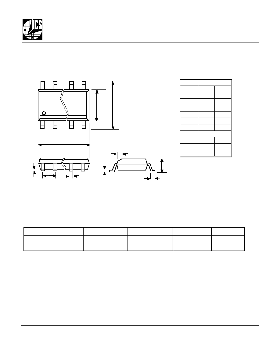
Package Outline and Package Dimensions
Ordering Information
Part/Order Number
Marking
Package
Shipping
Temperature
ICS650R-05
ICS650R-05
20 pin SSOP
Tubes
0 to 70 ∞C
ICS650R-05T
ICS650R-05
20 pin SSOP
Tape and Reel
0 to 70 ∞C
20 pin SSOP
Millimeters
Millimeters
Symbol
Min
Max
A
1.55
1.73
b
0.203
0.305
c
0.190
0.254
D
8.560
8.740
E
3.810
4.000
H
5.840
6.200
e 0.635 BSC
0.635 BSC
h
0.410
L
0.016
0.035
Q
0.127
0.250
While the information presented herein has been checked for both accuracy and reliability, Integrated Circuit Systems, Incorporated (ICS) assumes no responsibility for either its
use or for the infringement of any patents or other rights of third parties, which would result from its use. No other circuits, patents, or licenses are implied. This product is
intended for use in normal commercial applications. Any other applications such as those requiring extended temperature range, high reliability, or other extraordinary
environmental requirements are not recommended without additional processing by ICS. ICS reserves the right to change any circuitry or specifications without notice. ICS does
not authorize or warrant any ICS product for use in life support devices or critical medical instruments.
b
D
E
H
e
Q
c
h x 45∞
A
L