ICS650-11B
BroadCom Networking Clock Synthesizer
MDS 650-11B C
1
Revision 012005 Printed 11/14/04
Integrated Circuit Systems, Inc. ∑ 525 Race Street ∑ San Jose ∑ CA ∑ 95126∑(408)295-9800tel∑ www.icst.com
PRELIMINARY INFORMATION
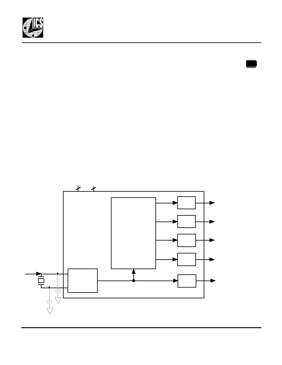
The ICS650-11B is a low cost, low jitter, high
performance clock synthesizer customized for
BroadCom. Using analog Phase-Locked Loop
(PLL) techniques, the device accepts a 25.0 MHz
clock or fundamental mode crystal input to
produce multiple output clocks of 25.0 MHz,
33.33 MHz, 66.66 MHz, 100.0 MHz, and
133.33 MHz. All output clocks are frequency
locked together. The ICS650-11B outputs all
have 0 ppm synthesis error.
Block Diagram
Description
Features
∑ Packaged in 20 pin narrow SSOP (Pb free available)
∑ 25.00 MHz fundamental crystal or clock input
∑ Five fixed output clocks of 25.0 MHz, 33.33 MHz,
66.66 MHz, 100.0 MHz, and 133.33 MHz
∑ Zero ppm synthesis error in all clocks
∑ Ideal for BroadCom BCM5600/BCM5400 chipset
∑ Full CMOS output swing
∑ Advanced, low power, sub-micron CMOS process
∑ 3.0V to 5.5V operating voltage
∑
Industrial temperature range
Clock
Buffer/
Crystal
Oscillator
VDD
GND
Clock Synthesis
and Control
Circuitry
133.33 MHz
25.00 MHz
crystal or clock
Output
Buffer
Output
Buffer
66.66 MHz
25.00 MHz
3
5
Output
Buffer
100.0 MHz
Output
Buffer
X1
X2
Output
Buffer
33.33 MHz
Optional crystal capacitors are shown and may be required for tuning of initial accuracy (determined once per board).
ICS650-11B
BroadCom Networking Clock Synthesizer
MDS 650-11B C
2
Revision 012005 Printed 11/14/04
Integrated Circuit Systems, Inc. ∑ 525 Race Street ∑ San Jose ∑ CA ∑ 95126∑(408)295-9800tel∑ www.icst.com
PRELIMINARY INFORMATION
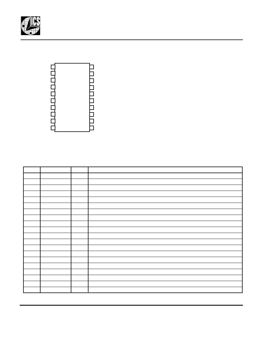
Pin Descriptions
Key: XI, XO = crystal connections; O = Output; P = power supply connection
Number
Name
Type
Description
1
GND
P
Connect to ground.
2
X2
XO
Crystal connection. Connect to 25 MHz crystal or leave unconnected for a clock input.
3
X1
XI
Crystal connection. Connect to 25 MHz fundamental crystal or clock input.
4
VDD
P
Connect to +3.3 V or +5 V. Must be same as other VDDs.
5
GND
P
Connect to ground.
6
GND
P
Connect to ground.
7
DC
-
Don't Connect. Do not connect anything to this pin.
8
DC
-
Don't Connect. Do not connect anything to this pin.
9
DC
-
Don't Connect. Do not connect anything to this pin.
10
100M
O
100.0 MHz clock output.
11
GND
P
Connect to ground.
12
66.66M
O
66.66 MHz clock output.
13
25M
O
25.0 MHz clock output.
14
GND
P
Connect to ground.
15
VDD
P
Connect to +3.3V or +5V. Must be same as other VDDs.
16
VDD
P
Connect to +3.3 V or +5 V. Must be same as other VDDs.
17
33.33M
O
33.33 MHz clock output.
18
133.33M
O
133.33 MHz clock output.
19
DC
-
Don't Connect. Do not connect anything to this pin.
20
DC
-
Don't Connect. Do not connect an thing to this pin.
Pin Assignment
1
16
2
3
4
15
14
13
VDD
D C
X2
VDD
20 pin (150 mil) SSOP
5
6
7
8
12
11
10
9
100M
D C
X1
GND
133.33M
D C
33.33M
66.66M
GND
D C
D C
18
17
19
20
GND
GND
25M
GND
VDD
ICS650-11B
BroadCom Networking Clock Synthesizer
MDS 650-11B C
3
Revision 012005 Printed 11/14/04
Integrated Circuit Systems, Inc. ∑ 525 Race Street ∑ San Jose ∑ CA ∑ 95126∑(408)295-9800tel∑ www.icst.com
PRELIMINARY INFORMATION
Parameter
Conditions
Minimum
Typical
Maximum
Units
ABSOLUTE MAXIMUM RATINGS (n
note 1)
Supply voltage, VDD
Referenced to GND
7
V
Inputs and Clock Outputs
Referenced to GND
-0.5
VDD+0.5
V
Ambient Operating Temperature
-40
85
∞C
Soldering Temperature
Max of 20 seconds
260
∞C
Storage temperature
-65
150
∞C
DC CHARACTERISTICS (VDD = 3.3V
V unless noted)
Operating Voltage, VDD
3
5.5
V
Input High Voltage, VIH, X1 pin only
VDD/2 + 1
VDD/2
V
Input Low Voltage, VIL, X1 pin only
VDD/2
VDD/2 - 1
V
Output High Voltage, VOH
IOH=-12mA
2.4
V
Output Low Voltage, VOL
IOL=12mA
0.4
V
Output High Voltage, VOH, CMOS level
IOH=-8mA
VDD-0.4
V
Operating Supply Current, IDD
No Load
35
mA
Short Circuit Current
Each output
±50
mA
AC CHARACTERISTICS (VDD = 3.3V
V unless noted)
Input Frequency
25.000
M H z
Output Clock Rise Time
0.8 to 2.0V
1.5
ns
Output Clock Fall Time
2.0 to 0.8V
1.5
ns
Output Clock Duty Cycle, except 25 MHz
At VDD/2
45
50
55
%
Frequency error
All clocks
0
ppm
Absolute Jitter, short term
Variation from mean
175
ps
Electrical Specifications
Notes:
1. Stresses beyond those listed under Absolute Maximum Ratings could cause permanent damage to the device. Prolonged
exposure to levels above the operating limits but below the Absolute Maximums may affect device reliability.
External Components
The ICS650-11B requires a minimum number of external components for proper operation. Decoupling
capacitors of 0.01µF should be connected between each VDD and GND on Pins 4 and 6, and Pins 16 and
14, as close to the ICS650-11B as possible. A series termination resistor of 33
may be used for each clock
output. The 25.00 MHz crystal must be connected as close to the chip as possible. The crystal should be a
fundamental mode (do not use third overtone), parallel resonant. Crystal capacitors should be connected
from pins X1 to ground and X2 to ground to optimize the initial accuracy. The value of these capacitors is
given by the following equation, where C
L
is the crystal load capacitance: Crystal caps (pF) = (C
L
-6) x 2. So
for a crystal with 16 pF load capacitance, two 20 pF caps should be used.
ICS650-11B
BroadCom Networking Clock Synthesizer
MDS 650-11B C
4
Revision 012005 Printed 11/14/04
Integrated Circuit Systems, Inc. ∑ 525 Race Street ∑ San Jose ∑ CA ∑ 95126∑(408)295-9800tel∑ www.icst.com
PRELIMINARY INFORMATION
While the information presented herein has been checked for both accuracy and reliability, Integrated Circuit Systems, Inc (ICS) assumes no responsibility for either its use or for
the infringement of any patents or other rights of third parties, which would result from its use. No other circuits, patents, or licenses are implied. This product is intended for use
in normal commercial applications. Any other applications such as those requiring extended temperature range, high reliability, or other extraordinary environmental
requirements are not recommended without additional processing by ICS. ICS reserves the right to change any circuitry or specifications without notice. ICS does not authorize
or warrant any ICS product for use in life support devices or critical medical instruments.
Ordering Information
Part/Order Number
Marking
Shipping packaging
Package
Temperature
ICS650R-11I
ICS650R-11I
tubes
20 pin SSOP
-40 to +85∞C
ICS650R-11IT
ICS650R-11I
tape and reel
20 pin SSOP
-40 to +85∞C
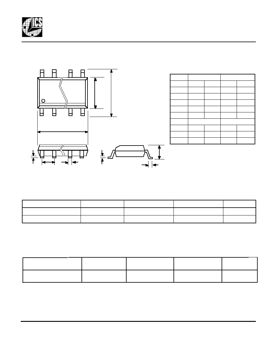
20 pin SSOP
Inchees
Millim
meters
Symbol
Min
Max
Min
Max
A
0.053
0.069
1.35
1.75
A1
0.004
0.010
0.102
0.254
b
0.008
0.012
0.203
0.305
c
0.007
0.010
0.191
0.254
D
0.337
0.344
8.560
8.738
e
.025 BSSC
0.635 B
BSC
E
0.228
0.244
5.791
6.198
E1
0.150
0.157
3.810
3.988
L
0.016
0.050
0.406
1.270
b
D
E1
E
e
A1
c
A
L
Package Outline and Package Dimensions
(
For current dimensional specifications, see JEDEC Publication No. 95.)
ICS650R-11ILF
ICS650R-11ILFT
ICS650R-11ILF
ICS650R-11ILF
tubes
tape and reel
20 pin SSOP
20 pin SSOP
-40 to +85∞C
-40 to +85∞C