ICS661
MDS 661 D
1
Revision 111804
Integrated Circuit Systems, Inc.
525 Race Street, San Jose, CA 95126
tel (408) 297-1201
www.icst.com
Precision Audio Clock Source
Description
The ICS661 provides synchronous clock generation for
audio sampling clock rates derived from an MPEG
stream, or can be used as a standalone clock source
with a 27 MHz crystal. The device uses the latest PLL
technology to provide excellent phase noise and long
term jitter performance for superior synchronization
and S/N ratio.
Please contact ICS if you have a requirement for an
input and output frequency not included here - we can
rapidly modify this product to meet special
requirements.
Features
∑
Packaged in 16-pin TSSOP
∑
Available in Pb (lead) fere package
∑
Clock or crystal input
∑
Low phase noise
∑
Low jitter
∑
Exact (0 ppm) multiplication ratios
∑
Reference clock output available
∑
Support for 256, 384, 512, and 768 times sampling
rate
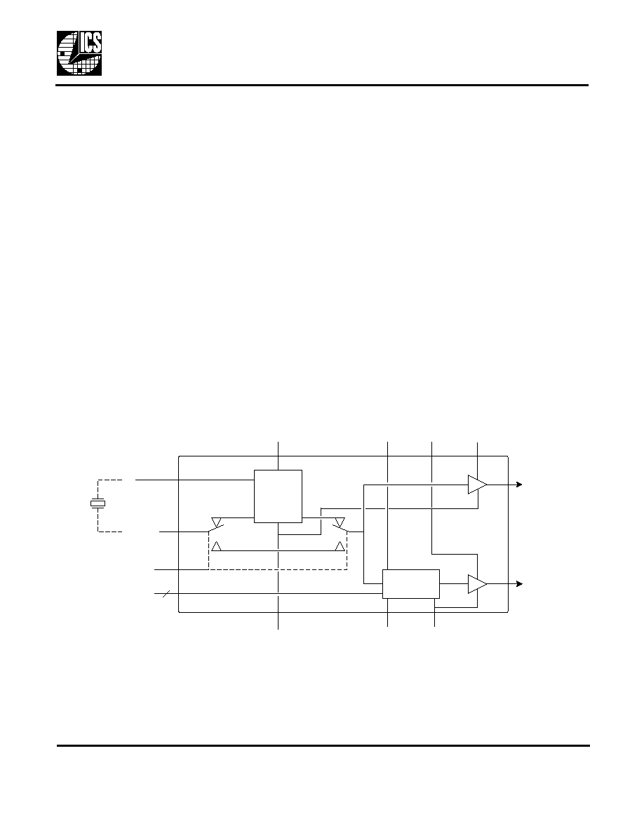
Block Diagram
PLL Clock
Synthesis
SELIN
Crystal
Oscillator
X2
X1/REFIN
VDD (P2)
VDDR
REF
CLK
GND (P13)
GND (P6)
GND (P5)
S3:0
4
VDD (P3)
VDDO
Precision Audio Clock Source
MDS 661 D
2
Revision 111804
Integrated Circuit Systems, Inc.
525 Race Street, San Jose, CA 95126
tel (408) 297-1201
www.icst.com
ICS661
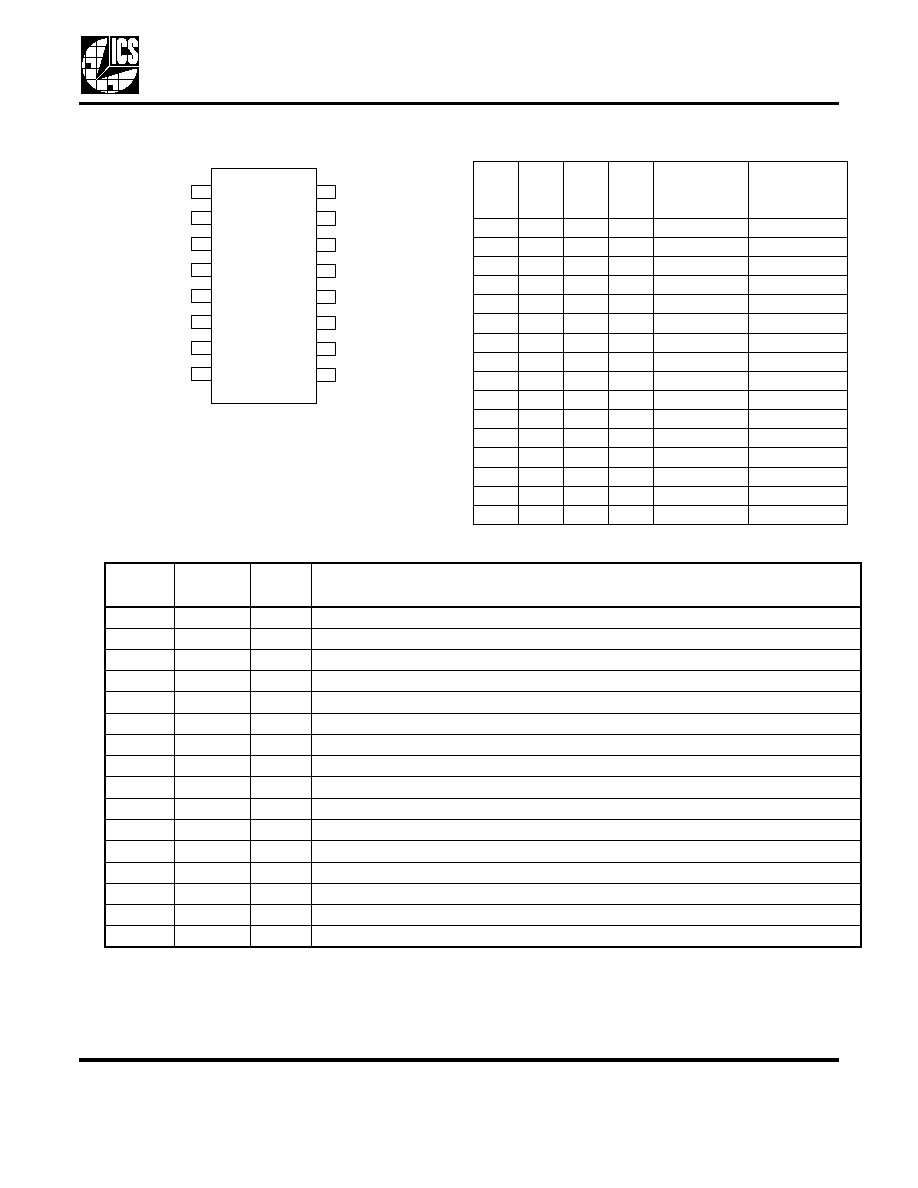
Pin Assignment
16-pin 4.40 mil body, 0.50 mm pitch TSSOP
Output Clock Selection Table
Pin Descriptions
12
1
11
2
10
X1/REFIN
X2
3
9
VDD
4
VDD
REF
5
S0
6
VDDR
7
GND
8
GND
GND
SELIN
VDDO
S3
S1
S2
CLK
16
15
14
13
S3
S2
S1
S0
Input
Frequency
(MHz)
Output
Frequency
(MHz)
0
0
0
0
27
8.192
0
0
0
1
27
11.2896
0
0
1
0
27
12.288
0
0
1
1
27
24.576
0
1
0
0
27
12.288
0
1
0
1
27
16.9344
0
1
1
0
27
18.432
0
1
1
1
27
36.864
1
0
0
0
27
16.384
1
0
0
1
27
22.5792
1
0
1
0
27
24.576
1
0
1
1
27
49.152
1
1
0
0
27
24.576
1
1
0
1
27
33.8688
1
1
1
0
27
36.864
1
1
1
1
27
73.728
Pin
Number
Pin
Name
Pin
Type
Pin Description
1
X1/REFIN
Input
Connect this pin to a crystal or clock input
2
VDD
Power
Power supply for crystal oscillator.
3
VDD
Power
Power supply for PLL.
4
S0
Input
Output frequency selection. Determines output frequency per table above. On chip pull-up.
5
GND
Power
Connect to ground.
6
GND
Power
Ground for output stage.
7
S3
Input
Output frequency selection. Determines output frequency per table above. On chip pull-up.
8
S2
Input
Output frequency selection. Determines output frequency per table above. On chip pull-up.
9
CLK
Output
Clock output.
10
S1
Input
Output frequency selection. Determines output frequency per table above. On chip pull-up.
11
VDDO
Power
Power supply for output stage.
12
SELIN
Input
Low for clock input, high for crystal. On chip pull-up.
13
GND
Power
Connect to ground.
14
VDDR
Power
Power supply for reference output. Ground to turn off REF.
15
REF
Output
Reference clock output.
16
X2
Input
Connect this pin to a crystal. Leave open if using a clock input.

Precision Audio Clock Source
MDS 661 D
3
Revision 111804
Integrated Circuit Systems, Inc.
525 Race Street, San Jose, CA 95126
tel (408) 297-1201
www.icst.com
ICS661
Application Information
Series Termination Resistor
Clock output traces should use series termination. To
series terminate a 50
trace (a commonly used trace
impedance), place a 33
resistor in series with the
clock line, as close to the clock output pin as possible.
The nominal impedance of the clock output is 20
.
Decoupling Capacitors
As with any high performance mixed-signal IC, the
ICS661 must be isolated from system power supply
noise to perform optimally.
Decoupling capacitors of 0.01µF must be connected
between each VDD and the PCB ground plane. To
further guard against interfering system supply noise,
the ICS661 should use one common connection to the
PCB power plane as shown in the diagram on the next
page. The ferrite bead and bulk capacitor help reduce
lower frequency noise in the supply that can lead to
output clock phase modulation.
Recommended Power Supply Connection for
Optimal Device Performance
All power supply pins must be connected to the same
voltage, except VDDR and VDDO may be connected to
a lower voltage in order to change the output level. If
the reference output is not used, ground VDDR.
Crystal Load Capacitors
If a crystal is used, the device crystal connections
should include pads for capacitors from X1 to ground
and from X2 to ground. These capacitors are used to
adjust the stray capacitance of the board to match the
nominally required crystal load capacitance. To reduce
possible noise pickup, use very short PCB traces (and
no vias) been the crystal and device.
The value of the load capacitors can be roughly
determined by the formula C = 2(C
L
- 6) where C is the
load capacitor connected to X1 and X2, and C
L
is the
specified value of the load capacitance for the crystal.
A typical crystal C
L
is 18 pF, so C = 2(18 - 6) = 24 pF.
Because these capacitors adjust the stray capacitance
of the PCB, check the output frequency using your final
layout to see if the value of C should be changed.
PCB Layout Recommendations
For optimum device performance and lowest output
phase noise, the following guidelines should be
observed.
1) Each 0.01µF decoupling capacitor should be
mounted on the component side of the board as close
to the VDD pin as possible. No vias should be used
between decoupling capacitor and VDD pin. The PCB
trace to VDD pin should be kept as short as possible,
as should the PCB trace to the ground via. Distance of
the ferrite bead and bulk decoupling from the device is
less critical.
2) The external crystal should be mounted next to the
device with short traces. The X1 and X2 traces should
not be routed next to each other with minimum spaces,
instead they should be separated and away from other
traces.
3) To minimize EMI and obtain the best signal integrity,
the 33
series termination resistor should be placed
close to the clock output.
4) An optimum layout is one with all components on the
same side of the board, minimizing vias through other
signal layers (the ferrite bead and bulk decoupling
capacitor can be mounted on the back). Other signal
traces should be routed away from the ICS661. This
includes signal traces just underneath the device, or on
layers adjacent to the ground plane layer used by the
device.
C onnec tion to 3.3V
P ow er P lane
Ferrite
B ead
B ulk D ec oupling C apac itor
(suc h as 1
F Tantalum )
V D D P in
V D D P in
V D D P in
0.01
F D ecoupling C apacitors

Precision Audio Clock Source
MDS 661 D
4
Revision 111804
Integrated Circuit Systems, Inc.
525 Race Street, San Jose, CA 95126
tel (408) 297-1201
www.icst.com
ICS661
Absolute Maximum Ratings
Stresses above the ratings listed below can cause permanent damage to the ICS661. These ratings, which
are standard values for ICS commercially rated parts, are stress ratings only. Functional operation of the
device at these or any other conditions above those indicated in the operational sections of the
specifications is not implied. Exposure to absolute maximum rating conditions for extended periods can
affect product reliability. Electrical parameters are guaranteed only over the recommended operating
temperature range.
Recommended Operation Conditions
DC Electrical Characteristics
Unless stated otherwise, VDD = 3.3 V ±10%, Ambient Temperature -40 to +85
∞C
Item
Rating
Supply Voltage, VDD
5.5 V
All Inputs and Outputs
-0.5 V to VDD+0.5 V
Ambient Operating Temperature
-40 to +85
∞C
Storage Temperature
-65 to +150
∞C
Junction Temperature
125
∞C
Soldering Temperature
260
∞C
Parameter
Min.
Typ.
Max.
Units
Ambient Operating Temperature
-40
+85
∞C
Power Supply Voltage (measured in respect to GND)
+3.0
+3.6
V
Parameter
Symbol
Conditions
Min.
Typ.
Max.
Units
Operating Voltage
VDD
3.0
3.6
V
VDDO
1.8
VDD
V
VDDR
1.8
VDD
V
Input High Voltage
V
IH
2
V
Input Low Voltage
V
IL
0.8
V
Output High Voltage
V
OH
I
OH
= -4 mA
VDD-0.4
V
Output High Voltage
V
OH
I
OH
= -20 mA
2.4
V
Output Low Voltage
V
OL
I
OL
= 20 mA
0.4
V
Supply Current
IDD
No Load
25
mA
Short Circuit Current
I
OS
Each output
±65
mA
Nominal Output Impedance
Z
OUT
20
Input Capacitance
Input pins
7
pF
Internal Pull-up Resistor
120
k

Precision Audio Clock Source
MDS 661 D
5
Revision 111804
Integrated Circuit Systems, Inc.
525 Race Street, San Jose, CA 95126
tel (408) 297-1201
www.icst.com
ICS661
AC Electrical Characteristics
Unless stated otherwise, VDD = 3.3 V ±10%, Ambient Temperature -40 to +85
∞C
Thermal Characteristics
Parameter
Symbol
Conditions
Min.
Typ.
Max.
Units
Crystal Frequency
27
28
MHz
Output Clock Rise Time
t
OR
20% to 80%, 15 pF load
1.5
ns
Output Clock Fall Time
t
OF
80% to 20%, 15 pF load
1.5
ns
Output Duty Cycle
t
OD
At VDD/2, 15 pF load
45
49 to 51
55
%
Jitter, Short term
Reference clock off
175
ps p-p
Jitter, Short term
Reference clock on
175
ps p-p
Jitter, Long term
Reference clock off; 10
us delay
300
ps p-p
Jitter, Long term
Reference clock on; 10
us delay
300
ps p-p
Single Sideband Phase
Noise
Reference clock off; 10
kHz offset
-110
dBc
Single Sideband Phase
Noise
Reference clock on; 10
kHz offset
-110
dBc
Actual Mean Frequency
Error versus Target
0
ppm
Parameter
Symbol
Conditions
Min.
Typ.
Max.
Units
Thermal Resistance Junction to
Ambient
JA
Still air
78
∞C/W
JA
1 m/s air flow
70
∞C/W
JA
3 m/s air flow
68
∞C/W
Thermal Resistance Junction to Case
JC
37
∞C/W
Precision Audio Clock Source
MDS 661 D
6
Revision 111804
Integrated Circuit Systems, Inc.
525 Race Street, San Jose, CA 95126
tel (408) 297-1201
www.icst.com
ICS661
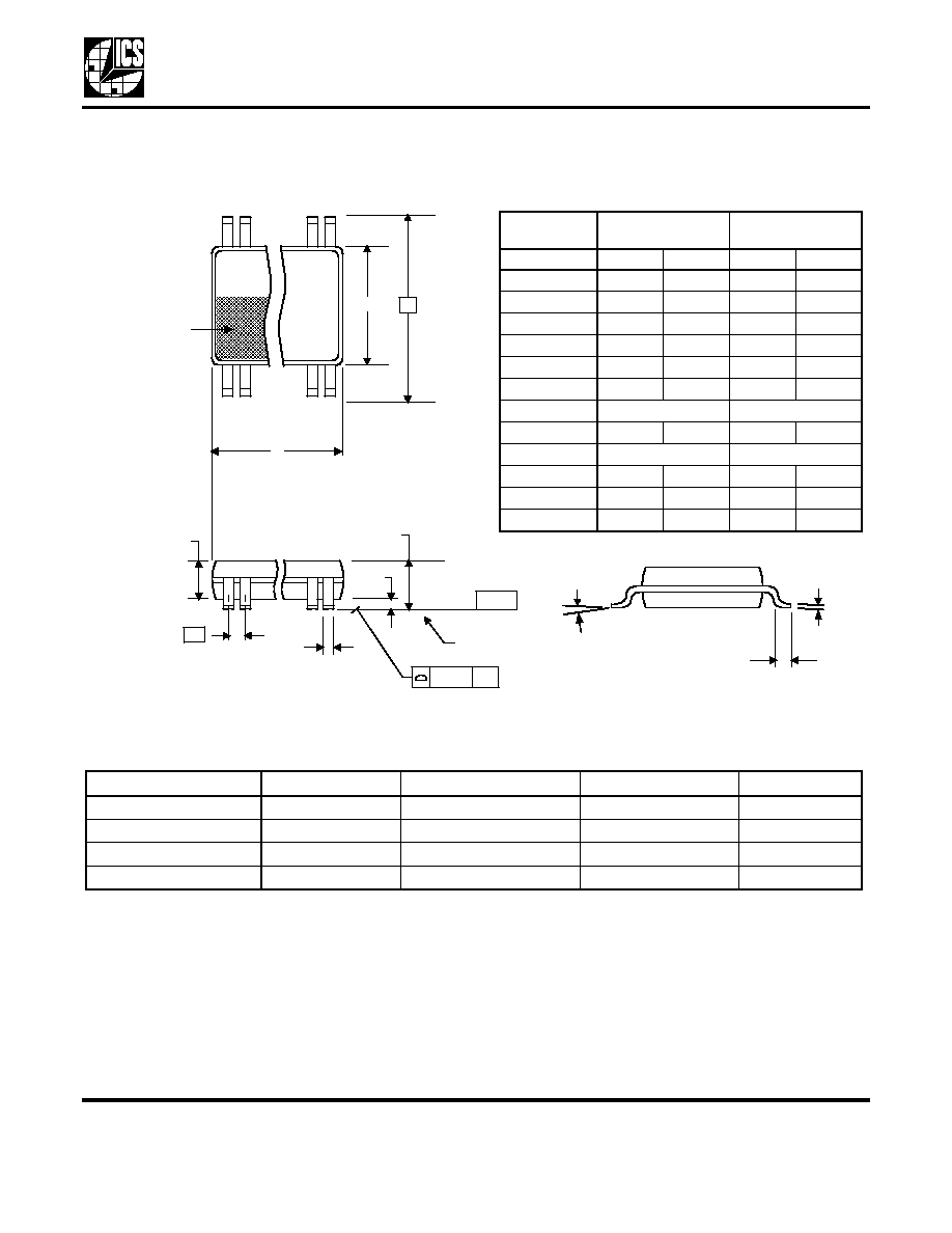
Package Outline and Package Dimensions
(16-pin TSSOP, 4.40 mm Body, 0.50 mm Pitch)
Package dimensions are kept current with JEDEC Publication No. 95, MO-153
Ordering Information
While the information presented herein has been checked for both accuracy and reliability, Integrated Circuit Systems (ICS)
assumes no responsibility for either its use or for the infringement of any patents or other rights of third parties, which would
result from its use. No other circuits, patents, or licenses are implied. This product is intended for use in normal commercial
applications. Any other applications such as those requiring extended temperature range, high reliability, or other extraordinary
environmental requirements are not recommended without additional processing by ICS. ICS reserves the right to change any
circuitry or specifications without notice. ICS does not authorize or warrant any ICS product for use in life support devices or
critical medical instruments.
Part / Order Number
Marking
Shipping Packaging
Package
Temperature
ICS661GI
ICS661GI
Tubes
16-pin TSSOP
-40 to +85
∞C
ICS661GITR
ICS661GI
Tape and Reel
16-pin TSSOP
-40 to +85
∞C
ICS661GILF
661GILF
Tubes
16-pin TSSOP
-40 to +85
∞C
ICS661GILFTR
661GILF
Tape and Reel
16-pin TSSOP
-40 to +85
∞C
INDEX
AREA
1 2
16
D
E1
E
SEATING
PLANE
A1
A
A2
e
- C -
b
aaa
C
c
L
Millimeters
Inches
Symbol
Min
Max
Min
Max
A
--
1.20
--
0.047
A1
0.05
0.15
0.002
0.006
A2
0.80
1.05
0.032
0.041
b
0.19
0.30
0.007
0.012
C
0.09
0.20
0.0035
0.008
D
4.90
5.1
0.193
0.201
E
6.40 BASIC
0.252 BASIC
E1
4.30
4.50
0.169
0.177
e
0.65 Basic
0.0256 Basic
L
0.45
0.75
0.018
0.030
0
∞
8
∞
0
∞
8
∞
aaa
--
0.10
--
0.004