 | –≠–ª–µ–∫—Ç—Ä–æ–Ω–Ω—ã–π –∫–æ–º–ø–æ–Ω–µ–Ω—Ç: ICS671-15 | –°–∫–∞—á–∞—Ç—å:  PDF PDF  ZIP ZIP |
ICS671-15
MDS 671-15 B
1
Revision 021904
I n t e gra t e d C i r c u i t S y s t e m s
5 2 5 R a c e S t r e e t , S a n J o s e, C A 9 5 1 2 6
t e l ( 4 0 8 ) 2 9 7 - 1 2 0 1
w w w. i c s t . c o m
Z
ERO
D
ELAY
, L
OW
S
KEW
B
UFFER
Description
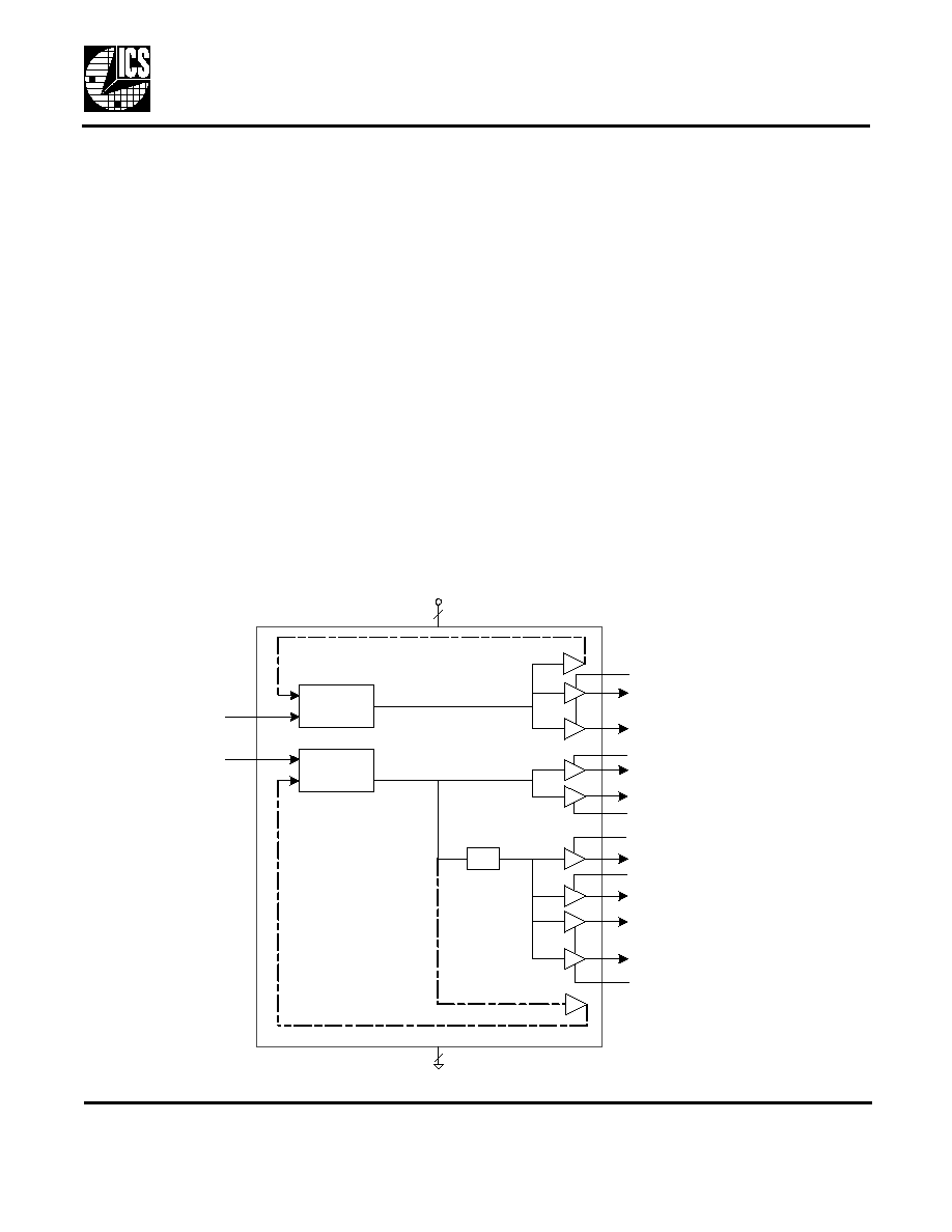
The ICS671-15 is a low-jitter, low-skew,
high-performance zero delay buffer (ZDB) for
high-speed applications. The device is designed using
ICS' proprietary low-jitter PLL (Phase-Locked Loop)
techniques. The ICS671-15 includes a ZDB bank of
four outputs running at 33 MHz, and two outputs at 66
MHz from the CPU PLL. This device also provides two
66 MHz zero delay clocks derived from the AGP PLL. In
the zero delay mode, the rising edge of the input clock
is aligned with the rising edges of the feedback clock.
The ICS671-15 provides feedback clocks internally for
the CPU PLL and the AGP PLL, and with the lowest
jitter.
Features
∑
Packaged in 24-pin TSSOP
∑
Input-output delay (±300 ps)
∑
Two ZDB 66 MHz outputs from a 66 MHz input AGP
clock
∑
Two ZDB 66 MHz outputs, plus four 33 MHz outputs
from a 33 MHz input CPU clock
∑
Output-to-output skew is less than 250 ps
∑
Full CMOS outputs with 18 mA output drive
capability at TTL levels (at 3.3 V)
∑
Spread Smart
TM
technology works with spread
spectrum clock generators
∑
Advanced, low-power, sub-micron CMOS process
∑
Operating voltage of 3.3 V
∑
Separate hardware output enable pins: OE1, OE2,
OE3, OE4, OE5 and OE6
Block Diagram
66M_AGPOUT2
AGP PLL
66M_IN
/2
VDD
4
GND
4
CPU PLL
33M_IN
OE4
OE1
OE5
OE6
OE2
OE3
66M_AGPOUT1
66M_CPUOUT1
66M_CPUOUT2
33M_PCIOUT1
33M_PCIOUT2
33M_PCIOUT3
33M_PCIOUT4
Z
ERO
D
ELAY
, L
OW
S
KEW
B
UFFER
MDS 671-15 B
2
Revision 021904
I n t e gr a t e d C i r c u i t S y s t e m s
5 2 5 R a c e S t r e e t , S a n J o s e, C A 9 5 1 2 6
t e l ( 4 0 8 ) 2 9 7 - 1 2 0 1
w w w. i c s t . c o m
ICS671-15
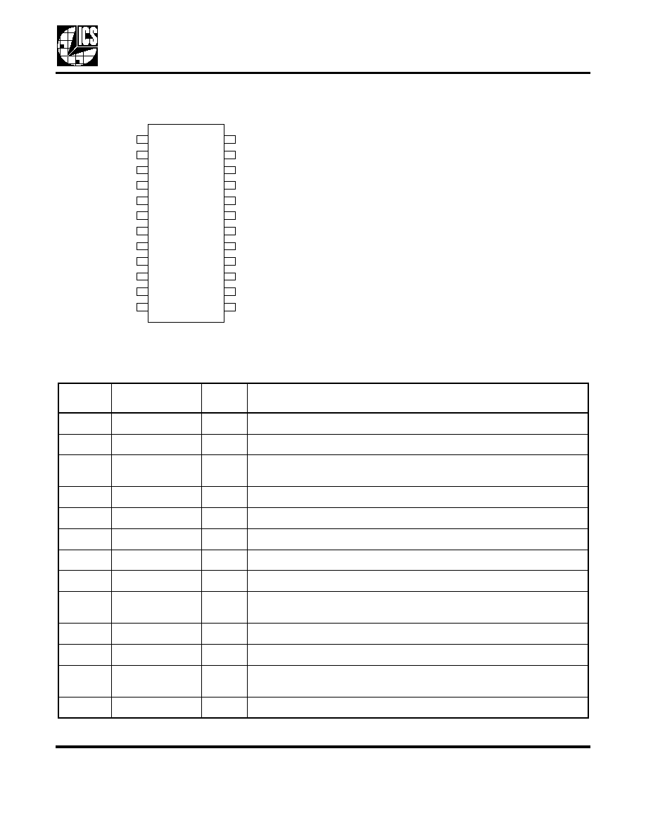
Pin Assignment
Pin Descriptions
20
1
19
2
18
33M_IN
66M_IN
3
17
VDD
4
16
OE5
OE6
5
15
GND
6
VDD
7
66M_CPUOUT1
8
GND
VDD
GND
VDD
OE4
9
10
OE3
OE1
GND
24
23
22
21
24-pin (173 mil) TSSOP
14
13
11
12
OE2
66M_CPUOUT2
33M_PCIOUT4
33M_PCIOUT3
33M_PCIOUT2
33M_PCIOUT1
66M_AGPOUT1
66M_AGPOUT2
Pin
Number
Pin
Name
Pin
Type
Pin Description
1
33M_IN
Input
Connect this pin to a 33 MHz input clock.
2
VDD
Power
Connect to +3.3 V.
3
OE5
Input
Output Enable control pin for outputs 66M_CPUOUT2. This pin is active
high and tri-states the outputs when low.
4
GND
Power
Connect to ground.
5
66M_CPUOUT1
Output
66 MHz output clock.
6
66M_CPUOUT2
Output
66 MHz output clock.
7
VDD
Power
Connect to +3.3 V.
8
VDD
Power
Connect to +3.3 V.
9
OE3
Input
Output Enable control pin for output 33M_PCIOUT4. This pin is active
high and tri-states the outputs when low.
10
33M_PCIOUT4
Output
33 MHz output clock.
11
33M_PCIOUT3
Output
33 MHz output clock.
12
OE2
Input
Output Enable control pin for output 33M_PCIOUT3. This pin is active
high and tri-states the outputs when low.
13
33M_PCIOUT2
Output
33 MHz output clock.

Z
ERO
D
ELAY
, L
OW
S
KEW
B
UFFER
MDS 671-15 B
3
Revision 021904
I n t e gr a t e d C i r c u i t S y s t e m s
5 2 5 R a c e S t r e e t , S a n J o s e, C A 9 5 1 2 6
t e l ( 4 0 8 ) 2 9 7 - 1 2 0 1
w w w. i c s t . c o m
ICS671-15
External Components
The ICS671-15 requires a minimum number of external components for proper operation. Decoupling
capacitors of 0.1
µF should be connected between VDD and GND, as close to the part as possible. A 33
series terminating resistor should be used on each clock output to reduce reflections.
Absolute Maximum Ratings
Stresses above the ratings listed below can cause permanent damage to the ICS671-15. These ratings,
which are standard values for ICS commercially rated parts, are stress ratings only. Functional operation of
the device at these or any other conditions above those indicated in the operational sections of the
specifications is not implied. Exposure to absolute maximum rating conditions for extended periods can
affect product reliability. Electrical parameters are guaranteed only over the recommended operating
temperature range.
14
33M_PCIOUT1
Output
33 MHz output clock.
15
GND
Power
Connect to ground.
16
OE1
Input
Output Enable control pin for output 33M_PCIOUT1 and
33M_PCIOUT2. This pin is active high and tri-states the outputs when
low.
17
OE4
Input
Output Enable control pin for outputs 66M_CPUOUT1. This pin is active
high and tri-states the outputs when low.
18
GND
Power
Connect to ground.
19
GND
Power
Connect to ground.
20
66M_AGPOUT1
Output
66 MHz output clock.
21
66M_AGPOUT2
Output
66 MHz output clock.
22
VDD
Power
Connect to +3.3 V.
23
OE6
Input
Output Enable control pin for outputs 66M_AGPOUT1 and
66M_AGPOUT2. This pin is active high and tri-states the outputs when
low.
24
66M_IN
Input
COnnect this pin to a 66 MHz input clock.
Pin
Number
Pin
Name
Pin
Type
Pin Description
Item
Rating
Supply Voltage, VDD
7 V
All Inputs and Outputs
-0.5 V to VDD+0.5 V
Ambient Operating Temperature
0 to +70
∞C
Storage Temperature
-65 to +150
∞C
Junction Temperature
125
∞C
Soldering Temperature
260
∞C

Z
ERO
D
ELAY
, L
OW
S
KEW
B
UFFER
MDS 671-15 B
4
Revision 021904
I n t e gr a t e d C i r c u i t S y s t e m s
5 2 5 R a c e S t r e e t , S a n J o s e, C A 9 5 1 2 6
t e l ( 4 0 8 ) 2 9 7 - 1 2 0 1
w w w. i c s t . c o m
ICS671-15
Recommended Operation Conditions
DC Electrical Characteristics
VDD=3.3 V ±5%, Ambient temperature 0 to +70
∞C
AC Electrical Characteristics
VDD = 3.3 V ±5%, Ambient Temperature 0 to +70
∞ C, CL=15 pF (Total)
Parameter
Min.
Typ.
Max.
Units
Ambient Operating Temperature
0
+70
∞C
Power Supply Voltage (measured in respect to GND)
+3.135
3.3
+3.465
V
Parameter
Symbol
Conditions
Min.
Typ.
Max.
Units
Operating Voltage
VDD
3.135
3.3
3.465
V
Input High Voltage
V
IH
66M, 33M,
OE1:OE6
2.0
V
Input Low Voltage
V
IL
66M, 33M
OE1:OE6
0.8
V
Output High Voltage
V
OH
I
OH
= -12 mA
2.4
V
Output Low Voltage
V
OL
I
OL
= 12 mA
0.4
V
Output High Voltage
V
OH
I
OH
= -4 mA
VDD-0.4
V
Operating Supply Current
66M, 33M Input
IDD
No Load. both
inputs active
32
mA
Short Circuit Current
I
OS
Each output
±50
mA
Input Capacitance
C
IN
5
pF
Parameter
Symbol
Conditions
Min.
Typ.
Max.
Units
Input Frequency
F
IN
33
66
MHz
Output Frequency
F
OUT
33
66
MHz
Output Rise Time
t
OR
0.8 to 2.0 V
1.5
ns
Output Fall Time
t
OF
2.0 to 0.8 V
1.5
ns
Output Clock Duty Cycle
at VDD/2
45
50
55
%
Device-to-Device Skew
Rising edges at VDD/2
for similar outputs,
Note 1
500
700
ps
Output-to-Output Skew
t
S
Rising edges at VDD/2
66M AGP outputs,
Note 1
250
500
ps

Z
ERO
D
ELAY
, L
OW
S
KEW
B
UFFER
MDS 671-15 B
5
Revision 021904
I n t e gr a t e d C i r c u i t S y s t e m s
5 2 5 R a c e S t r e e t , S a n J o s e, C A 9 5 1 2 6
t e l ( 4 0 8 ) 2 9 7 - 1 2 0 1
w w w. i c s t . c o m
ICS671-15
Note 1: All outputs are equally loaded.
Thermal Characteristics
Output-to-Output Skew
t
S
Rising edges at VDD/2
66M CPU outputs,
Note 1
250
500
ps
Output-to-Output Skew
t
S
Rising edges at VDD/2
33M PCI outputs,
Note 1
300
500
ps
Skew from output of 66M CPU to
33M PCI, equally loaded
t
S
Rising edges at VDD/2
33M PCI outputs
300
500
ps
Short-term Jitter
t
JA
pealk-to-peak
300
ps
Input-to-Output Delay
t
D
measured at VDD/2
-500
+500
ps
PLL Lock Time
t
LOCK
Stable power supply,
valid clocks on 66M and
33M
1
ms
Output Enable Time
(for OE1 to E6)
OE going from low to
high with stable output
1.0
ns
Output Disable Time
(for OE1 to E6)
OE going high to low
tri-state output
1.0 ns
Parameter
Symbol
Conditions
Min.
Typ.
Max.
Units
Thermal Resistance Junction to
Ambient
JA
Still air
77
∞C/W
JA
1 m/s air flow
68
∞C/W
JA
2 m/s air flow
66
∞C/W
Thermal Resistance Junction to Case
JC
25
∞C/W
Parameter
Symbol
Conditions
Min.
Typ.
Max.
Units
ICS671-15
MDS 671-15 B
6
Revision 021904
I n t e gra t e d C i r c u i t S y s t e m s
5 2 5 R a c e S t r e e t , S a n J o s e, C A 9 5 1 2 6
t e l ( 4 0 8 ) 2 9 7 - 1 2 0 1
w w w. i c s t . c o m
Z
ERO
D
ELAY
, L
OW
S
KEW
B
UFFER
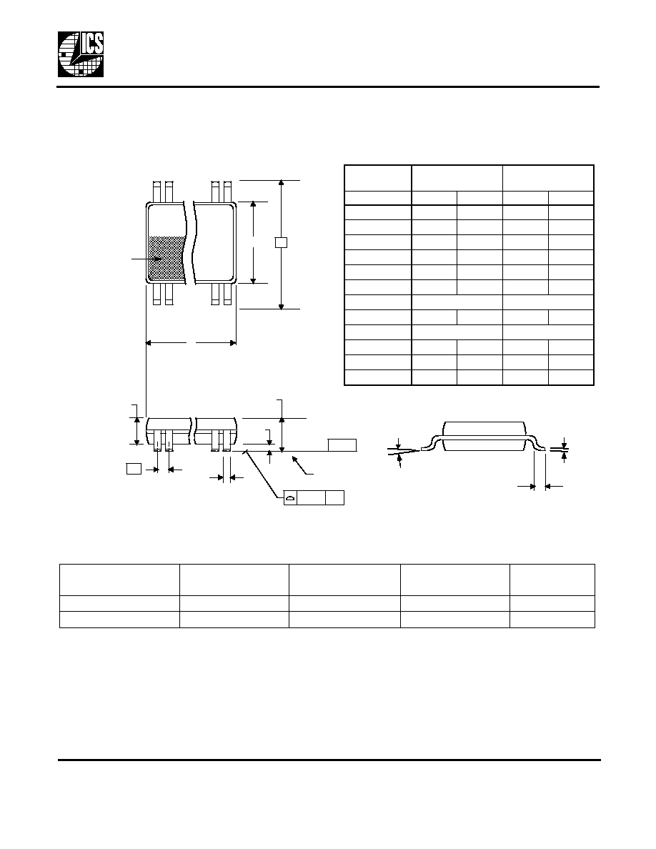
Package Outline and Package Dimensions
(24-pin TSSOP, 4.4mm Body)
Package dimensions are kept current with JEDEC Publication No. 95
Ordering Information
While the information presented herein has been checked for both accuracy and reliability, Integrated Circuit
Systems (ICS) assumes no responsibility for either its use or for the infringement of any patents or other rights of
third parties, which would result from its use. No other circuits, patents, or licenses are implied. This product is
intended for use in normal commercial applications. Any other applications such as those requiring extended
temperature range, high reliability, or other extraordinary environmental requirements are not recommended
without additional processing by ICS. ICS reserves the right to change any circuitry or specifications without notice.
ICS does not authorize or warrant any ICS product for use in life support devices or critical medical instruments.
Part / Order Number
Marking
Shipping
Packaging
Package
Temperature
ICS671G-15
ICS671G-15
Tubes
24-pin TSSOP
0 to 70
∞ C
ICS671G-15T
ICS671G-15
Tape and Reel
24-pin TSSOP
0 to 70
∞ C
INDEX
AREA
1 2
24
D
E1
E
SEATING
PLANE
A1
A
A2
e
- C -
b
aaa
C
c
L
Millimeters
Inches
Symbol
Min
Max
Min
Max
A
--
1.20
--
0.047
A1
0.05
0.15
0.002
0.006
A2
0.80
1.05
0.032
0.041
b
0.19
0.30
0.007
0.012
C
0.09
0.20
0.0035
0.008
D
7.70
7.90
0.303
0.311
E
6.40 BASIC
0.252 BASIC
E1
4.30
4.50
0.169
0.177
e
0.65 Basic
0.0256 Basic
L
0.45
0.75
0.018
0.030
0
∞
8
∞
0
∞
8
∞
aaa
--
0.10
--
0.004