 | –≠–ª–µ–∫—Ç—Ä–æ–Ω–Ω—ã–π –∫–æ–º–ø–æ–Ω–µ–Ω—Ç: ICS673 | –°–∫–∞—á–∞—Ç—å:  PDF PDF  ZIP ZIP |
ICS673-01
MDS 673-01 I
1
Revision 051203
I n t e g r a t e d C i r cu i t S y st e m s
q
5 2 5 Ra ce S t r e e t , S a n J o s e , C A 9 5 1 2 6
q
t e l ( 4 0 8 ) 2 9 5 - 9 8 0 0
q
w w w. i c s t . c o m
PLL B
UILDING
B
LOCK
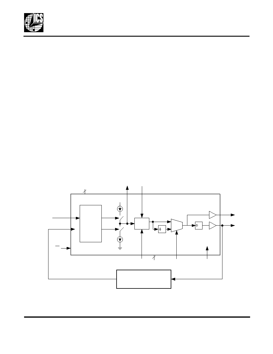
Description
The ICS673-01 is a low cost, high performance Phase
Locked Loop (PLL) designed for clock synthesis and
synchronization. Included on the chip are the phase
detector, charge pump, Voltage Controlled Oscillator
(VCO), and two output buffers. One output buffer is a
divide by two of the other. Through the use of external
reference and VCO dividers (the ICS674-01), the user
can customize the clock to lock to a wide variety of
input frequencies.
The ICS673-01 also has an output enable function that
puts both outputs into a high-impedance state. The
chip also has a power down feature which turns off the
entire device.
For applications that require low jitter or jitter
attenuation, see the MK2069. For a smaller package,
see the ICS663.
Features
∑
Packaged in 16 pin SOIC
∑
Access to VCO input and feedback paths of PLL
∑
VCO operating range up to 120 MHz (5V)
∑
Able to lock MHz range outputs to kHz range inputs
through the use of external dividers
∑
Output Enable tri-states outputs
∑
Low skew output clocks
∑
Power Down turns off chip
∑
VCO predivide to feedback divider of 1 or 4
∑
25 mA output drive capability at TTL levels
∑
Advanced, low power, sub-micron CMOS process
∑
Single supply +3.3 V or +5 V ±10% operating voltage
∑
Industrial temperature range available
∑
Forms a complete PLL, using the ICS674-01
∑
For better jitter performance, please use the MK1575
Block Diagram
REFIN
Phase/
Frequency
Detector
VCO
4
2
SEL
VCOIN
CHCP
UP
FBIN
DOWN
I
cp
I
cp
CLK2
VDD
MUX
1
0
External Feedback Divider
(such as the ICS674-01)
Clock Input
CAP
PD
(entire chip)
VDD
2
3
GND
CLK1
OE
(both
outputs)
PLL B
UILDING
B
LOCK
MDS 673-01 I
2
Revision 051203
I n t e g r a t e d C i r c u i t S y s t e ms
q
5 2 5 R a c e S t r e e t , S a n J o s e , CA 9 5 1 2 6
q
t e l ( 4 0 8 ) 2 9 5 - 9 8 0 0
q
w w w. ic s t . c o m
ICS673-01
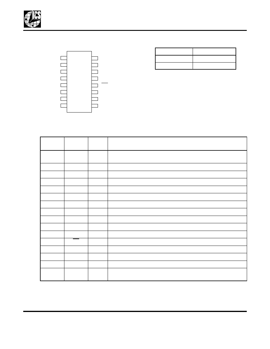
Pin Assignment
VCO Predivide Select Table
0 = connect pin directly to ground
1 = connect pin directly to VDD
Pin Descriptions
1 2
1
1 1
2
1 0
F B IN
R E F IN
3
9
V D D
4
V D D
N C
5
G N D
6
C L K 1
7
G N D
8
G N D
C L K 2
P D
S E L
C H G P
O E
V C O IN
C A P
1 6
1 5
1 4
1 3
1 6 p in n a rro w (1 5 0 m il) S O IC
SEL
VCO Predivide
0
4
1
1
Pin
Number
Pin
Name
Pin
Type
Pin Description
1
FBIN
Input
Feedback clock input. Connect the feedback clock to this pin. Falling
edge triggered.
2
VDD
Power
Connect to +3.3 V or +5 V and to VDD on pin 3.
3
VDD
Power
Connect to VDD on pin 2.
4
GND
Power
Connect to ground.
5
GND
Power
Connect to ground.
6
GND
Power
Connect to ground.
7
CHGP
Output
Charge pump output. Connect to VCOIN under normal operation.
8
VCOIN
Input
Input to internal VCO.
9
CAP
Input
Loop filter return.
10
OE
Input
Output enable. Active when high. Tri-states both outputs when low.
11
SEL
Input
Select pin for VCO predivide to feedback divider per table above.
12
PD
Input
Power down. Turns off entire chip when pin is low. Outputs stop low.
13
CLK2
Output
Clock output 2. Low skew divide by two version of CLK1.
14
CLK1
Output
Clock output 1.
15
NC
-
No connect. Nothing is connected internally to this pin.
16
REFIN
Input
Reference input. Connect reference clock to this pin. Falling edge is
triggered.
PLL B
UILDING
B
LOCK
MDS 673-01 I
3
Revision 051203
I n t e g r a t e d C i r c u i t S y s t e ms
q
5 2 5 R a c e S t r e e t , S a n J o s e , CA 9 5 1 2 6
q
t e l ( 4 0 8 ) 2 9 5 - 9 8 0 0
q
w w w. ic s t . c o m
ICS673-01
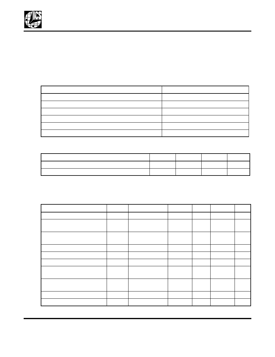
Absolute Maximum Ratings
Stresses above the ratings listed below can cause permanent damage to the ICS673-01. These ratings,
which are standard values for ICS commercially rated parts, are stress ratings only. Functional operation of
the device at these or any other conditions above those indicated in the operational sections of the
specifications is not implied. Exposure to absolute maximum rating conditions for extended periods can
affect product reliability. Electrical parameters are guaranteed only over the recommended operating
temperature range.
Recommended Operation Conditions
DC Electrical Characteristics
VDD=3.3V ±5% or 5.0V ±10%,
Ambient temperature -40 to +85
∞
C, unless stated otherwise
Item
Rating
Supply Voltage, VDD
7V
All Inputs and Outputs
-0.5V to VDD+0.5V
Ambient Operating Temperature
0 to +70
∞
C
Industrial Temperature
-40 to +85
∞
C
Storage Temperature
-65 to +150
∞
C
Soldering Temperature
260
∞
C
Parameter
Min.
Typ.
Max.
Units
Ambient Operating Temperature
0
+70
∞
C
Power Supply Voltage (measured in respect to GND)
+3.13
+5.25
V
Parameter
Symbol
Conditions
Min.
Typ.
Max.
Units
Operating Voltage
VDD
3.13
5.50
V
Logic Input High Voltage
V
IH
REFIN, FBIN,
SEL
2
V
Logic Input Low Voltage
V
IL
REFIN, FBIN,
SEL
0.8
V
LF Input Voltage Range
V
I
0
VDD
V
Output High Voltage
V
OH
I
OH
= -25 mA
2.4
V
Output Low Voltage
V
OL
I
OL
= 25mA
0.4
V
Output High Voltage, CMOS
level
V
OH
I
OH
= -8 mA
VDD-0.4
Operating Supply Current
IDD
VDD = 5.0 V,
No load, 40 MHz
15
mA
Short Circuit Current
I
OS
CLK
±100
mA
Input Capacitance
C
I
SEL
5
pF
PLL B
UILDING
B
LOCK
MDS 673-01 I
4
Revision 051203
I n t e g r a t e d C i r c u i t S y s t e ms
q
5 2 5 R a c e S t r e e t , S a n J o s e , CA 9 5 1 2 6
q
t e l ( 4 0 8 ) 2 9 5 - 9 8 0 0
q
w w w. ic s t . c o m
ICS673-01
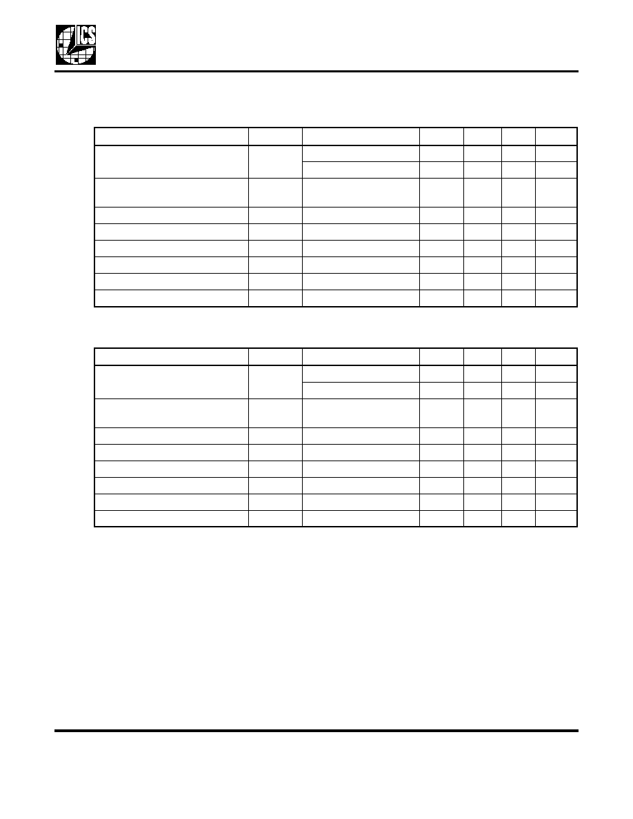
AC Electrical Characteristics
VDD = 3.3V ±5%,
Ambient Temperature -40 to +85
∞
C, C
LOAD
at CLK = 15 pF, unless stated otherwise
VDD = 5.0V ±10%,
Ambient Temperature -40 to +85
∞
C, C
LOAD
at CLK = 15 pF,
unless stated otherwise
Note 1: Minimum input frequency is limited by loop filter design. 1 kHz is a practical minimum limit.
External Components
The ICS673-01 requires a minimum number of external
components for proper operation. A decoupling
capacitor of 0.01
µ
F should be connected between
VDD and GND as close to the ICS673-01 as possible.
A series termination resistor of 33
may be used at
the clock output.
Special considerations must be made in choosing loop
components C
S
and C
P
. These can be found online at
http://www.icst.com/products/telecom/loopfiltercap.htm
Avoiding PLL Lockup
In some applications, the ICS673-01 can "lock up" at
the maximum VCO frequency. This is usually caused
by power supply glitches or a very slow power supply
ramp. This situation also occurs if the external divider
starts to fail at high input frequencies. The usual failure
mode of a divider circuit is that the output of the divider
begins to miss clock edges. The phase detector
interprets this as a too low output frequency and
Parameter
Symbol
Conditions
Min.
Typ.
Max.
Units
Output Clock Frequency
(from pin CLK)
f
CLK
SEL = 1
1
100
MHz
SEL = 0
0.25
25
MHz
Input Clock Frequency
(into pins REFIN or FBIN)
f
REF
Note 1
8
MHz
Output Rise Time
t
OR
0.8 to 2.0V
1.2
2
ns
Output Fall Time
t
OF
2.0 to 0.8V
0.75
1.5
ns
Output Clock Duty Cycle
t
DC
At VDD/2
40
50
60
%
Jitter, Absolute peak-to-peak
t
J
250
ps
VCO Gain
K
O
190
MHz/V
Charge Pump Current
I
cp
2.5
µ
A
Parameter
Symbol
Conditions
Min.
Typ.
Max.
Units
Output Clock Frequency
(from pin CLK)
f
CLK
SEL = 1
1
120
MHz
SEL = 0
0.25
30
MHz
Input Clock Frequency
(into pins REFIN or FBIN)
f
REF
Note 1
8
MHz
Output Rise Time
t
OR
0.8 to 2.0V
0.5
1
ns
Output Fall Time
t
OF
2.0 to 0.8V
0.5
1
ns
Output Clock Duty Cycle
t
DC
At VDD/2
45
50
55
%
Jitter, Absolute peak-to-peak
t
J
150
ps
VCO Gain
K
O
190
MHz/V
Charge Pump Current
I
cp
2.4
µ
A
PLL B
UILDING
B
LOCK
MDS 673-01 I
5
Revision 051203
I n t e g r a t e d C i r c u i t S y s t e ms
q
5 2 5 R a c e S t r e e t , S a n J o s e , CA 9 5 1 2 6
q
t e l ( 4 0 8 ) 2 9 5 - 9 8 0 0
q
w w w. ic s t . c o m
ICS673-01
increases the VCO frequency. The feedback divider
begins to miss even more clock edges and the VCO
frequency is continually increased until it is running at
its maximum frequency. Whether caused by power
supply issues or by the external divider, the loop can
only recover by powering down the circuit or asserting
PD.
The simplest way to avoid this problem is to use an
external divider that always operates correctly
regardless of the VCO speed. Figures 2 and 3 show
that the VCO is capable of high speeds. By using the
internal divide-by-four and/or the CLK2 output, the
maximum VCO frequency can be divided by 2, 4, or 8
and a slower counter can be used. Using the ICS673
internal dividers in this manner does reduce the
number of frequencies that can be exactly synthesized
by forcing the total VCO divide to change in increments
of 2, 4, or 8.
If this lockup problem occurs, there are several
solutions; three of which are described below.
1. If the system has a reset or power good signal, this
should be applied to the PD pin, forcing the chip to stay
powered down until the power supply voltage has
stabilized
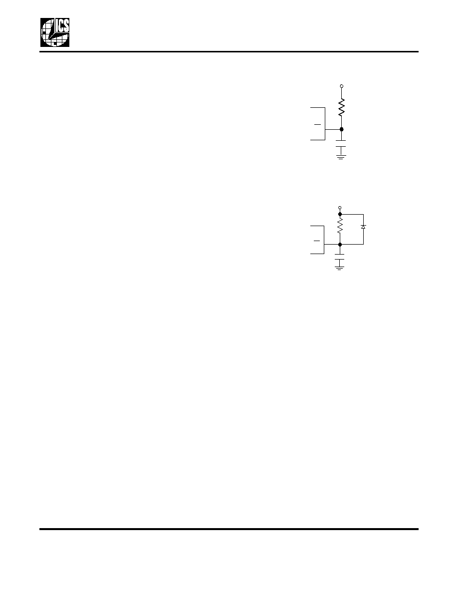
2. If no power good signal is available, a simple
power-on reset circuit can be attached to the PD pin, as
shown in Figure 1. When the power supply ramps up,
this circuit holds PD asserted (device powered down)
until the capacitor charges.
The circuit of Figure 1A is adequate in most cases, but
the discharge rate of capacitor C3 when VDD goes low
is limited by R1. As this discharge rate determines the
minimum reset time, the circuit of Figure 1B may be
used when a faster reset time is desired. The values of
R1 and C3 should be selected to ensure that PD stays
below 1.0 V until the power supply is stable.
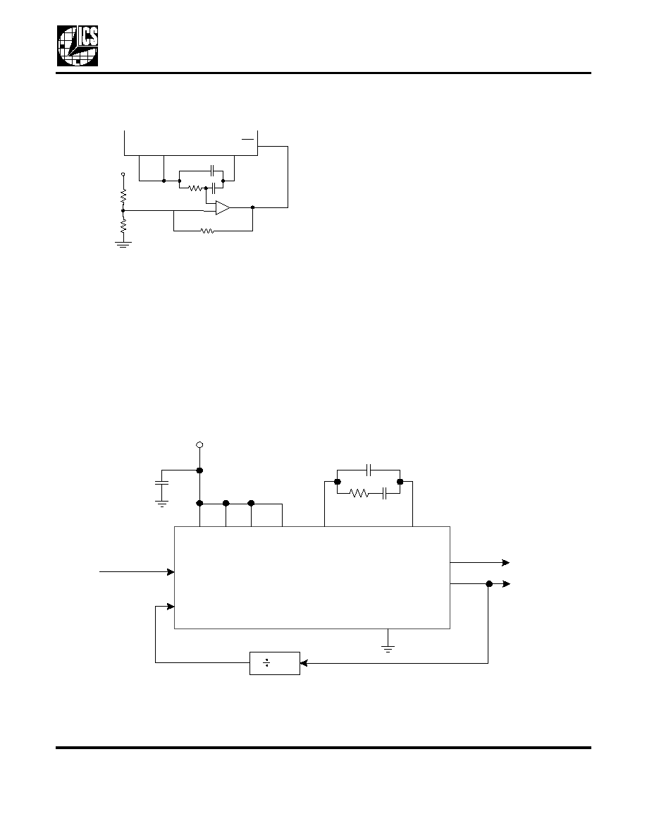
3. A comparator circuit may be used to monitor the loop
filter voltage as shown in Figure 2. This circuit will
dump the charge off the loop filter by asserting PD if the
VCO begins to run too fast and the PLL can recover. A
good choice for the comparator is the National
Semiconductor LMC7211BIM5X. It is low power,
version of the small (SOT-23), low cost, and has high
input impedance.
The trigger voltage of the comparator is set by the
voltage divider formed by R2 and R3. The voltage
should be set to a value higher than the VCO input is
expected to run during normal operation. Typically, this
A. Basi c Ci r cui t
R
1
C
3
PD
I CS673- 01
VDD
B . F a s t e r D i s c h a r g e
R
1
C
3
P D
I C S 6 7 3 - 0 1
V D D
D
1
F i g 1 . P o we r o n Re s e t Ci r c u i t s
PLL B
UILDING
B
LOCK
MDS 673-01 I
6
Revision 051203
I n t e g r a t e d C i r c u i t S y s t e ms
q
5 2 5 R a c e S t r e e t , S a n J o s e , CA 9 5 1 2 6
q
t e l ( 4 0 8 ) 2 9 5 - 9 8 0 0
q
w w w. ic s t . c o m
ICS673-01
might be 0.5 V below VDD. Hysteresis should be
added to the circuit by connecting R4.
The CLK output frequency may be up to 2x the
maximum Output Clock Frequency listed in the AC
Electrical Characteristics above when the device is in
an unlocked condition. Make sure that the external
divider can operate up to this frequency.
Explanation of Operation
The ICS673-01 is a PLL building block circuit that
includes an integrated VCO with a wide operating
range. The device uses external PLL loop filter
components which through proper configuration allow
for low input clock reference frequencies, such as a
15.7 kHz Hsync input.
The phase/frequency detector compares the falling
edges of the clocks inputted to FBIN and REFIN. It then
generates an error signal to the charge pump, which
produces a charge proportional to this error. The
external loop filter integrates this charge, producing a
voltage that then controls the frequency of the VCO.
This process continues until the edges of FBIN are
aligned with the edges of the REFIN clock, at which
point the output frequency will be locked to the input
frequency.
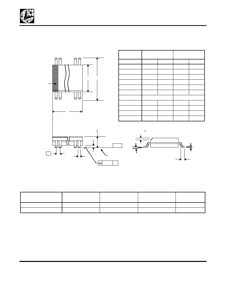
Figure 3. Example Configuration -- Generating a 20 MHz clock from a 200 kHz
reference.
Figure 2. Using an External Comparator
to Reset the VCO
CHGP VCOIN
R
Z
C
1
C
2
CAP
+
-
R
4
R
2
R
3
PD
ICS673-01
REFIN
+3.3 or 5 V
SEL
VDD
0.01
µ
F
FBIN
200 kHz
100
Digital Divider
such as ICS674-01
GND
CLK2
CAP
20 MHz
VCOIN
C
1
R
Z
C
2
200 kHz
OE PD
40 MHz
CLK1

PLL B
UILDING
B
LOCK
MDS 673-01 I
7
Revision 051203
I n t e g r a t e d C i r c u i t S y s t e ms
q
5 2 5 R a c e S t r e e t , S a n J o s e , CA 9 5 1 2 6
q
t e l ( 4 0 8 ) 2 9 5 - 9 8 0 0
q
w w w. ic s t . c o m
ICS673-01
Determining the Loop Filter Values
The loop filter components consist of C
S
, C
P
, and R
S
.
Calculating these values is best illustrated by an
example. Using the example in Figure 1, we can
synthesize 20 MHz from a 200 kHz input.
The phase locked loop may be approximately
described by the following equations:
Bandwidth
Damping factor,
where:
K
O
= VCO gain (Hz/V)
I
cp
= Charge pump current (A)
N = Total feedback divide from VCO,
including the internal VCO post divider
C
S
= Loop filter capacitor (Farads)
R
S
= Loop filter resistor (Ohms)
As a general rule, the bandwidth should be at least 20
times less than the reference frequency, i.e.,
In this example, using the above equation, bandwidth
should be less than or equal to 10 kHz. By setting the
bandwith to 10kHz and using the first equation, R
S
can
be determined since all other variables are known. In
the example of Figure 1, N = 200, comprising the divide
by 2 on the chip (VCO post divider) and the external
divide by 100. Therefore, the bandwidth equation
becomes:
and R
S
= 26 k
Choosing a damping factor of 0.7 (a minimal damping
factor than can be used to ensure fast lock time),
damping factor equation becomes:
and C
S
= 1.32 nF (1.2 nF is the nearest standard
value).
The capacitor C
P
is used to damp transients from the
charge pump and should be approximately 1/20th the
size of C
S
, i.e.,
Therefore, C
P
= 60 pF (56 pF nearest standard value).
To summarize, the loop filter components are:
C
S
= 1.2 nf
C
P
= 56 pf
R
S
= 26 k
When choosing either CLK1 or CLK2 to drive the
feedback divider, ICS recommends that CLK2 be used
so that the rising edges of CLK1, CLK2, and REFIN are
all synchronized. If CLK1 is used to feedback, CLK2
may be either a rising or falling edge when compared to
CLK1 and REFIN.
NBW
R
S
K
O
I
CP
2
N
----------------------------
=
R
S
2
------
K
O
I
CP
C
S
N
-----------------------------
=
BW
REFIN
(
)
20
/
10,000
R
S
190
10
6
2.5
10
6
≠
2
200
-------------------------------------------------------------
=
0.7
25 000
,
2
----------------
190 10
6
2.5 10
6
≠
C
S
200
----------------------------------------------------------------
=
C
P
C
S
20
/
PLL B
UILDING
B
LOCK
MDS 673-01 I
8
Revision 051203
I n t e g r a t e d C i r c u i t S y s t e ms
q
5 2 5 R a c e S t r e e t , S a n J o s e , CA 9 5 1 2 6
q
t e l ( 4 0 8 ) 2 9 5 - 9 8 0 0
q
w w w. ic s t . c o m
ICS673-01
Package Outline and Package Dimensions
(16 pin SOIC, 150 Mil. Narrow Body)
Package dimensions are kept current with JEDEC Publication No. 95
Ordering Information
While the information presented herein has been checked for both accuracy and reliability, Integrated Circuit Systems (ICS)
assumes no responsibility for either its use or for the infringement of any patents or other rights of third parties, which would
result from its use. No other circuits, patents, or licenses are implied. This product is intended for use in normal commercial
applications. Any other applications such as those requiring extended temperature range, high reliability, or other extraordinary
environmental requirements are not recommended without additional processing by ICS. ICS reserves the right to change any
circuitry or specifications without notice. ICS does not authorize or warrant any ICS product for use in life support devices or
critical medical instruments.
Part / Order Number
Marking
Shipping
packaging
Package
Temperature
ICS673M-01I
ICS673M-01
Tubes
16 pin SOIC
-40 to +85
∞
C
ICS673M-01IT
ICS673M-01
Tape and Reel
16 pin SOIC
-40 to +85
∞
C
INDEX
AREA
1 2
16
D
E
SEATING
PLANE
A1
A
e
- C -
B
.10 (.004)
C
C
L
H
h x 45
Millimeters
Inches
Symbol
Min
Max
Min
Max
A
1.35
1.75
.0532
.0688
A1
0.10
0.25
.0040
.0098
B
0.33
0.51
.013
.020
C
0.19
0.25
.0075
.0098
D
9.80
10.00
.3859
.3937
E
3.80
4.00
.1497
.1574
e
1.27 BASIC
0.050 BASIC
H
5.80
6.20
.2284
.2440
h
0.25
0.50
.010
.020
L
0.40
1.27
.016
.050
0
∞
8
∞
0
∞
8
∞