 | –≠–ª–µ–∫—Ç—Ä–æ–Ω–Ω—ã–π –∫–æ–º–ø–æ–Ω–µ–Ω—Ç: ICS722 | –°–∫–∞—á–∞—Ç—å:  PDF PDF  ZIP ZIP |
MDS 722 A
1
Revision 121404
I n t e gra t e d C i r c u i t S y s t e m s
5 2 5 R a c e S t r e e t , S a n J o s e, C A 9 5 1 2 6
t e l ( 4 0 8 ) 2 9 7 - 1 2 0 1
w w w. i c s t . c o m
L
OW
C
OST
27 MH
Z
3.3 V
OLT
VCXO
ICS722
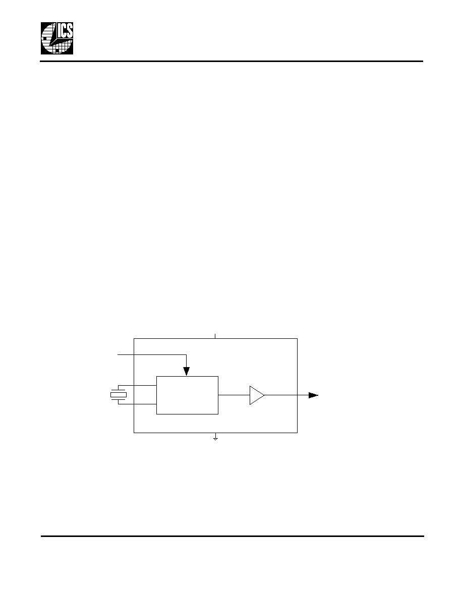
Description
The ICS722 is a low cost, low-jitter, high-performance
3.3 volt VCXO designed to replace expensive discrete
VCXOs modules. The on-chip Voltage Controlled
Crystal Oscillator accepts a 0 to 3.3 V input voltage to
cause the output clocks to vary by over ±100 ppm.
Using ICS' patented VCXO techniques, the device
uses an inexpensive external pullable crystal in the
range of 16.2 to 28 MHz to produce a VCXO output
clock at that same frequency.
The frequency of the on-chip VCXO is adjusted by an
external control voltage input into pin VIN. Because
VIN is a high-impedance input, it can be driven directly
from an PWM RC integrator circuit. Frequency output
increases with VIN voltage input. The usable range of
VIN is 0 to 3.3 V.
ICS manufactures the largest variety of Set-Top Box
and multimedia clock synthesizers for all applications.
Consult ICS to eliminate VCXOs, crystals, and
oscillators from your board.
Features
∑
Packaged in 8-pin SOIC
∑
Operational frequency range of 16.2 MHz to 28 MHz
∑
Uses an inexpensive external crystal
∑
On-chip patented VCXO with pull range of 230 ppm
(minimum)
∑
VCXO tuning voltage of 0 to 3.3 V
∑
Operating voltage of 3.3 V
∑
12 mA output drive capability at TTL levels
∑
Advanced, low-power, sub-micron CMOS process
Block Diagram
X1
X2
Voltage
Controlled
Crystal
Oscillator
VIN
16.2-28MHz
Pullable
Crystal
16.2-28MHz Clock
(REFOUT)
GND
VDD

L
OW
C
OST
27 MH
Z
3.3 V
OLT
VCXO
MDS 722 A
2
Revision 121404
I n t e gr a t e d C i r c u i t S y s t e m s
5 2 5 R a c e S t r e e t , S a n J o s e, C A 9 5 1 2 6
t e l ( 4 0 8 ) 2 9 7 - 1 2 0 1
w w w. i c s t . c o m
ICS722
Pin Assignment
Pin Descriptions
X 1
V D D
V I N
D C
G N D
R E F O U T
D C
X 2
1
2
3
4
8
7
6
5
I C S 7 2 2
8 - P i n ( 1 5 0 m i l ) S O I C
Pin
Number
Pin
Name
Pin
Type
Pin Description
1
XI
Input
Crystal connection. Connect to the external pullable crystal.
2
VDD
Power
Connect to +3.3 V (0.01
µf decoupling capacitor recommended).
3
VIN
Input
Voltage input to VCXO. Zero to 3.3 V signal which controls the
VCXO frequency.
4
GND
Power
Connect to ground.
5
REFOUT
Output
VCXO CMOS level clock output matches the nominal frequency of
the crystal.
6
DC
--
Do not connect anything to this pin.
7
DC
--
Do not connect anything to this pin.
8
X2
Input
Crystal connection. Connect to a external pullable crystal.
L
OW
C
OST
27 MH
Z
3.3 V
OLT
VCXO
MDS 722 A
3
Revision 121404
I n t e gr a t e d C i r c u i t S y s t e m s
5 2 5 R a c e S t r e e t , S a n J o s e, C A 9 5 1 2 6
t e l ( 4 0 8 ) 2 9 7 - 1 2 0 1
w w w. i c s t . c o m
ICS722
External Component Selection
The ICS722 requires a minimum number of external
components for proper operation.
Decoupling Capacitors
A decoupling capacitor of 0.01
µF should be connected
between VDD and GND on pins 2 and 4 as close to the
ICS722 as possible. For optimum device performance,
the decoupling capacitor should be mounted on the
component side of the PCB. Avoid the use of vias in the
decoupling circuit.
Series Termination Resistor
When the PCB trace between the clock output and the
load is over 1 inch, series termination should be used.
To series terminate a 50
trace (a commonly used
trace impedance), place a 33
resistor in series with
the clock line, as close to the clock output pin as
possible. The nominal impedance of the clock output is
20
.
Quartz Crystal
The ICS722 VCXO function consists of the external
crystal and the integrated VCXO oscillator circuit. To
assure the best system performance (frequency pull
range) and reliability, a crystal device with the
recommended parameters (shown below) must be
used, and the layout guidelines discussed in the
following section shown must be followed.
The oscillation frequency of a quartz crystal is
determined by its "cut" and by the load capacitors
connected to it. The ICS722 incorporates on-chip
variable load capacitors that "pull" (change) the
frequency of the crystal. The crystal specified for use
with the ICS722 is designed to have zero frequency
error when the total of on-chip + stray capacitance is
14 pF.
Recommended Crystal Parameters:
Initial Accuracy at 25
∞
C
±20 ppm
Temperature Stability
±30 ppm
Aging
±20 ppm
Load Capacitance
14 pf
Shunt Capacitance, C0
7 pF Max
C0/C1 Ratio
250 Max
Equivalent Series Resistance
35
Max
The external crystal must be connected as close to the
chip as possible and should be on the same side of the
PCB as the ICS722. There should be no via's between
the crystal pins and the X1 and X2 device pins. There
should be no signal traces underneath or close to the
crystal. See application note MAN05.
Crystal Tuning Load Capacitors
The crystal traces should include pads for small fixed
capacitors, one between X1 and ground, and another
between X2 and ground. Stuffing of these capacitors
on the PCB is optional. The need for these capacitors is
determined at system prototype evaluation, and is
influenced by the particular crystal used (manufacture
and frequency) and by PCB layout. The typical required
capacitor value is 1 to 4 pF.
The procedure for determining the value of these
capacitors can be found in application note MAN05.
L
OW
C
OST
27 MH
Z
3.3 V
OLT
VCXO
MDS 722 A
4
Revision 121404
I n t e gr a t e d C i r c u i t S y s t e m s
5 2 5 R a c e S t r e e t , S a n J o s e, C A 9 5 1 2 6
t e l ( 4 0 8 ) 2 9 7 - 1 2 0 1
w w w. i c s t . c o m
ICS722
Absolute Maximum Ratings
Stresses above the ratings listed below can cause permanent damage to the ICS722. These ratings, which
are standard values for ICS commercially rated parts, are stress ratings only. Functional operation of the
device at these or any other conditions above those indicated in the operational sections of the
specifications is not implied. Exposure to absolute maximum rating conditions for extended periods can
affect product reliability. Electrical parameters are guaranteed only over the recommended operating
temperature range.
Recommended Operation Conditions
DC Electrical Characteristics
VDD=3.3 V ±5%
, Ambient temperature 0 to +70
∞C, unless stated otherwise
Item
Rating
Supply Voltage, VDD
7 V
All Inputs and Outputs
-0.5 V to VDD+0.5 V
Ambient Operating Temperature
0 to +70
∞C
Storage Temperature
-65 to +150
∞C
Soldering Temperature
260
∞C
Parameter
Min.
Typ.
Max.
Units
Ambient Operating Temperature
0
≠
+70
∞C
Power Supply Voltage (measured in respect to GND)
+3.15
+3.45
V
Reference crystal parameters
Refer to page 3
Parameter
Symbol
Conditions
Min.
Typ.
Max.
Units
Operating Voltage
VDD
3.15
3.45
V
Output High Voltage
V
OH
I
OH
= -12 mA
2.4
V
Output Low Voltage
V
OL
I
OL
= 12 mA
0.4
V
Output High Voltage (CMOS
Level)
V
OH
I
OH
= -4 mA
VDD-0.4
V
Operating Supply Current
IDD
No load
6
mA
Short Circuit Current
I
OS
±50
mA
VIN, VCXO Control Voltage
V
IA
0
3.3
V

L
OW
C
OST
27 MH
Z
3.3 V
OLT
VCXO
MDS 722 A
5
Revision 121404
I n t e gr a t e d C i r c u i t S y s t e m s
5 2 5 R a c e S t r e e t , S a n J o s e, C A 9 5 1 2 6
t e l ( 4 0 8 ) 2 9 7 - 1 2 0 1
w w w. i c s t . c o m
ICS722
AC Electrical Characteristics
VDD = 3.3 V ±5%, Ambient Temperature 0 to +70
∞ C, unless stated otherwise
Note 1: External crystal device must conform with Pullable Crystal Specifications listed on page 3.
Thermal Characteristics
Marking Diagram (ICS722M)
Marking Diagram (ICS722MLF)
Notes:
1. ###### is the lot number.
2. YYWW is the last two digits of the year and week that the part was assembled.
3. "LF" denotes Pb (lead) free package.
4. Bottom marking: (origin)
Origin = country of origin if not USA.
Parameter
Symbol
Conditions
Min.
Typ.
Max.
Units
Output Frequency
F
O
16.2
28
MHz
Crystal Pullability
F
P
0V< VIN < 3.3 V, Note 1
+ 115
ppm
VCXO Gain
VIN = VDD/2 + 1 V, Note 1
120
ppm/V
Output Rise Time
t
OR
0.8 to 2.0 V, C
L
=15 pF
1.5
ns
Output Fall Time
t
OF
2.0 to 0.8 V, C
L
=15 pF
1.5
ns
Output Clock Duty
Cycle
t
D
Measured at 1.4 V, C
L
=15 pF
40
50
60
%
Maximum Output
Jitter, short term
t
J
C
L
=15 pF
110
ps
Parameter
Symbol
Conditions
Min.
Typ.
Max.
Units
Thermal Resistance Junction to
Ambient
JA
Still air
150
∞C/W
JA
1 m/s air flow
140
∞C/W
JA
3 m/s air flow
120
∞C/W
Thermal Resistance Junction to Case
JC
40
∞C/W
ICS722M
######
YYWW
1
4
5
8
722MLF
######
YYWW
1
4
5
8
L
OW
C
OST
27 MH
Z
3.3 V
OLT
VCXO
MDS 722 A
6
Revision 121404
I n t e gr a t e d C i r c u i t S y s t e m s
5 2 5 R a c e S t r e e t , S a n J o s e, C A 9 5 1 2 6
t e l ( 4 0 8 ) 2 9 7 - 1 2 0 1
w w w. i c s t . c o m
ICS722
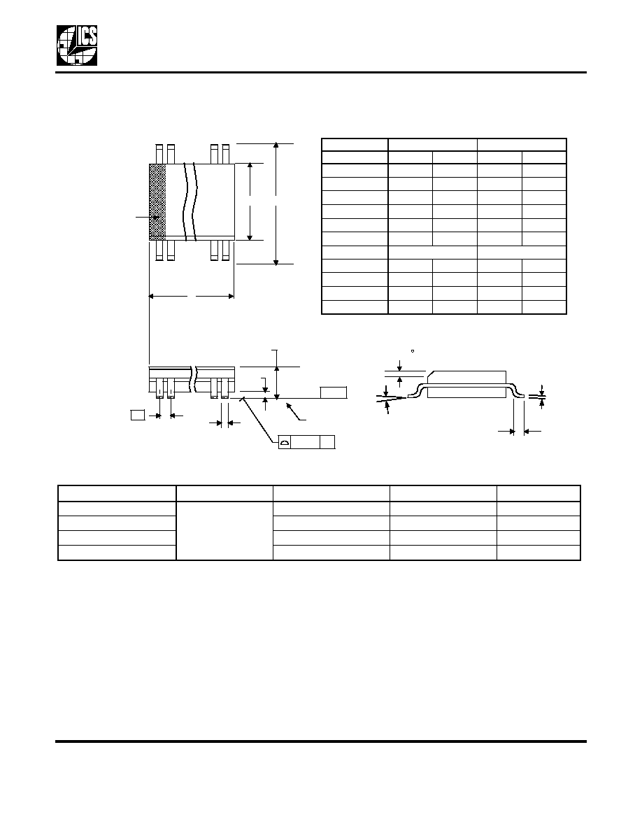
Package Outline and Package Dimensions
(8-pin SOIC)
Package dimensions are kept current with JEDEC Publication No. 95
Ordering Information
"LF" denotes Pb (lead) free package.
While the information presented herein has been checked for both accuracy and reliability, Integrated Circuit Systems (ICS)
assumes no responsibility for either its use or for the infringement of any patents or other rights of third parties, which would
result from its use. No other circuits, patents, or licenses are implied. This product is intended for use in normal commercial
applications. Any other applications such as those requiring extended temperature range, high reliability, or other extraordinary
environmental requirements are not recommended without additional processing by ICS. ICS reserves the right to change any
circuitry or specifications without notice. ICS does not authorize or warrant any ICS product for use in life support devices or
critical medical instruments.
Part / Order Number
Marking
Shipping Packaging
Package
Temperature
ICS722M
see page 5
Tubes
8-pin SOIC
0 to +70
∞ C
ICS722MT
Tape and Reel
8-pin SOIC
0 to +70
∞ C
ICS722MLF
Tubes
8-pin SOIC
0 to +70
∞ C
ICS722MLFT
Tape and Reel
8-pin SOIC
0 to +70
∞ C
INDEX
AREA
1 2
8
D
E
SEATING
PLANE
A1
A
e
- C -
B
.10 (.004)
C
C
L
H
h x 45
Millimeters
Inches
Symbol
Min
Max
Min
Max
A
1.35
1.75
0.0532
0.0688
A1
1.10
0.25
0.0040
0.0098
B
0.33
0.51
0.013
0.020
C
0.19
0.25
0.0075
0.0098
D
4.80
5.00
.1890
.1968
E
3.80
4.00
0.1497
0.1574
e
1.27 Basic
0.050 Basic
H
5.80
6.20
0.2284
0.2440
h
0.25
0.50
0.010
0.020
L
0.40
1.27
0.016
0.050
a
0
∞
8
∞
0
∞
8
∞