 | –≠–ª–µ–∫—Ç—Ä–æ–Ω–Ω—ã–π –∫–æ–º–ø–æ–Ω–µ–Ω—Ç: ICS726 | –°–∫–∞—á–∞—Ç—å:  PDF PDF  ZIP ZIP |
ICS726
MDS 726 F
1
Revision 112905
I n t e gra t e d C i r c u i t S y s t e m s
5 2 5 R a c e S t r e e t , S a n J o s e, C A 9 5 1 2 6
t e l ( 4 0 8 ) 2 9 7 - 1 2 0 1
w w w. i c s t . c o m
12
TO
36 MH
Z
SOT-23 VCXO
Description
Used in conjunction with an external pullable quartz
crystal, this monolithic integrated circuit replaces more
costly hybrid (canned) VCXO devices. The ICS726 is
designed primarily for data and clock recovery
applications such as ADSL modems, set-top box
receivers, and telecom systems.
The frequency of the on-chip VCXO is adjusted by an
external control voltage to the VIN pin. Since VIN is a
high impedance input, it can be driven directly from an
PWM RC integrator circuit. Frequency output increases
with VIN voltage input. The usable range of VIN is 0 to
3.3 V.
Features
∑
Uses an inexpensive 12 to 36 MHz external crystal
∑
Output frequency range of 12 to 36 MHz
∑
On-chip VCXO with guaranteed pull range of ±115
ppm minimum
∑
VCXO tuning voltage 0 to 3.3 V
∑
Packaged in 6-pin TSOT-23-6
∑
Available in Pb (lead) free package
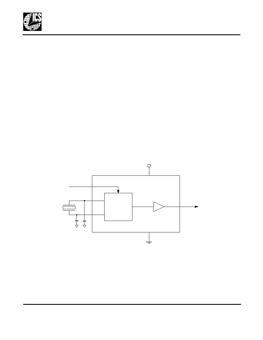
Block Diagram
Voltage
Controlled
Crystal
Oscillator
12-36MHz
Pullable
Crystal
X1
X2
VIN
12-36MHz
VDD
GND
12
TO
36 MH
Z
SOT-23 VCXO
MDS 726 F
2
Revision 112905
I n t e gr a t e d C i r c u i t S y s t e m s
5 2 5 R a c e S t r e e t , S a n J o s e, C A 9 5 1 2 6
t e l ( 4 0 8 ) 2 9 7 - 1 2 0 1
w w w. i c s t . c o m
ICS726
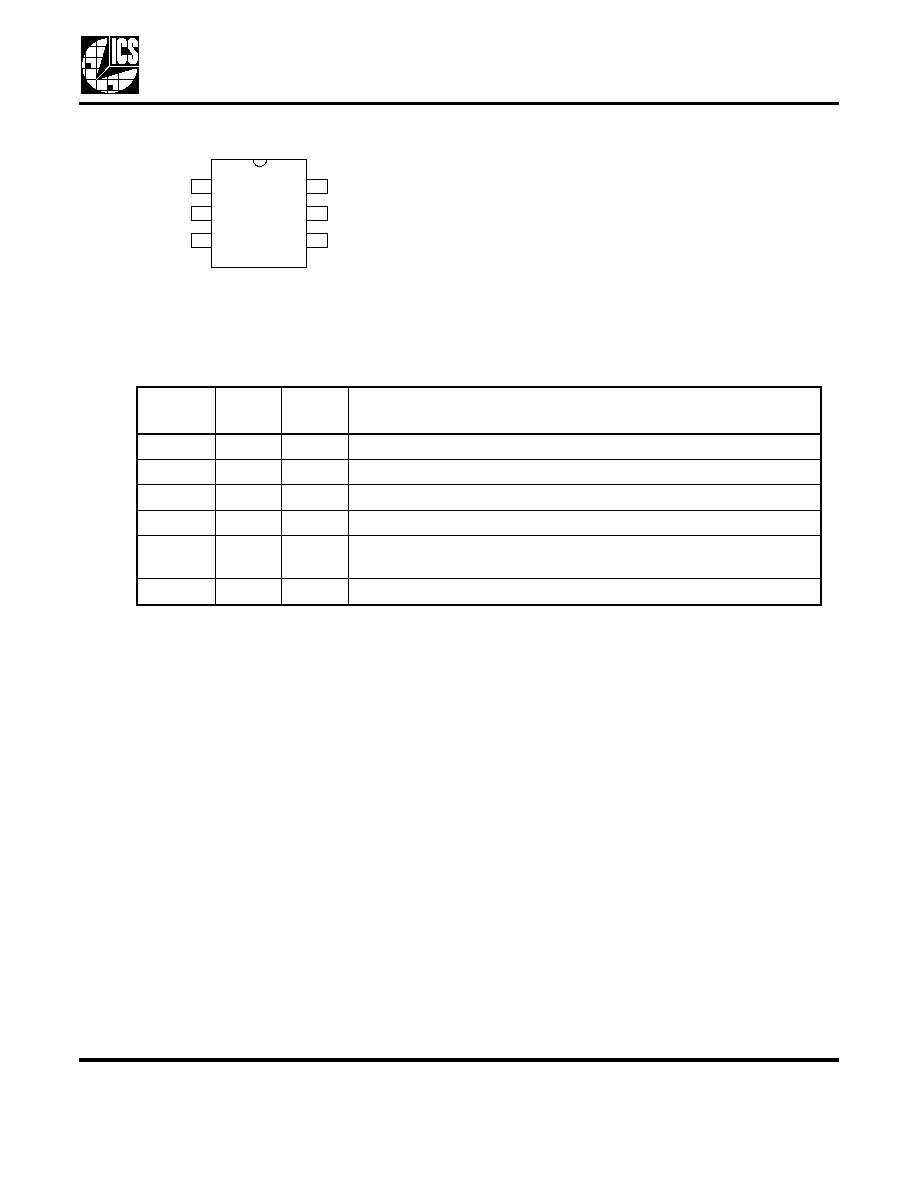
Pin Assignment
Pin Descriptions
X 2
G N D
C L K
V I N
V D D
X 1
1
2
3
6
5
4
T S OT - 2 3 - 6
Pin
Number
Pin
Name
Pin
Type
Pin Description
1
X2
Input
Crystal connection. Connect to the external pullable crystal.
2
GND
Power
Connect to ground.
3
CLK
Output
VCXO CMOS level clock output at the frequency of the crystal.
4
VDD
Power
Connect to +3.3 V (0.01uf decoupling capacitor recommended).
5
VIN
Input
Voltage input to VCXO -- 0 to 3.3 V analog input which controls the
oscillation frequency of the VCXO.
6
XI
Input
Crystal connection. Connect to the external pullable crystal.

12
TO
36 MH
Z
SOT-23 VCXO
MDS 726 F
3
Revision 112905
I n t e gr a t e d C i r c u i t S y s t e m s
5 2 5 R a c e S t r e e t , S a n J o s e, C A 9 5 1 2 6
t e l ( 4 0 8 ) 2 9 7 - 1 2 0 1
w w w. i c s t . c o m
ICS726
External Component Selection
The ICS726 requires a minimum number of external
components for proper operation.
Decoupling Capacitor
A decoupling capacitor of 0.01µF must be connected
between VDD (pin 4) and GND (pin 2), as close to
these pins as possible. For optimum device
performance, the decoupling capacitor should be
mounted on the component side of the PCB. Avoid the
use of vias in the decoupling circuit.
Series Termination Resistor
When the PCB trace between the clock output (CLK,
pin 3) and the load is over 1 inch, series termination
should be used. To series terminate a 50
trace (a
commonly used trace impedance) place a 33
resistor
in series with the clock line, as close to the clock output
pin as possible. The nominal impedance of the clock
output is 20
.
Quartz Crystal
The ICS726 VCXO function consists of the external
crystal and the integrated VCXO oscillator circuit. To
assure the best system performance (frequency pull
range) and reliability, a crystal device with the
recommended parameters (shown below) must be
used, and the layout guidelines discussed in the
following section shown must be followed.
The frequency of oscillation of a quartz crystal is
determined by its "cut" and by the load capacitors
connected to it. The ICS726 incorporates on-chip
variable load capacitors that "pull" (change) the
frequency of the crystal. The crystal specified for use
with the ICS726 is designed to have zero frequency
error when the total of on-chip + stray capacitance is 14
pF.
Required Crystal Parameters:
Nominal Frequency
as required MHz
Initial Accuracy at 25
∞
C
-20 min/+20 max ppm
Temperature Stability
-30 min/+30 max ppm
Aging, 1st year
-5 min/+5 max ppm
Aging, 10 years
-20 min/+20 max ppm
Operating Temp. Range, ∞C
0 min/+25 typ/+70 max
or
Operating Temp. Range, ∞C
-40 min/+25 typ/+85 max
Load Capacitance
10 pf
Shunt Capacitance, C0
7 pF Max
C0/C1 Ratio
270 Max
Equivalent Series Resistance
35
Max
The third overtone mode of the crystal and all spurs
must be >100 ppm distant from the 3x fundamental
resonance measured with a physical load of 10 pF.
The external crystal must be connected as close to the
chip as possible and should be on the same side of the
PCB as the ICS726. There should be no vias between
the crystal pins and the X1 and X2 device pins. There
should be no signal traces underneath or close to the
crystal. See application note MAN05.
Crystal Tuning Load Capacitors
The crystal traces should include pads for small fixed
capacitors, one between X1 and ground, and another
between X2 and ground. The need for these capacitors
is determined at system prototype evaluation, and is
influenced by the particular crystal used (manufacture
and frequency) and by PCB layout. The typical required
capacitor value is 1 to 4 pF.
The procedure for determining the value of these
capacitors can be found in application note MAN05.
12
TO
36 MH
Z
SOT-23 VCXO
MDS 726 F
4
Revision 112905
I n t e gr a t e d C i r c u i t S y s t e m s
5 2 5 R a c e S t r e e t , S a n J o s e, C A 9 5 1 2 6
t e l ( 4 0 8 ) 2 9 7 - 1 2 0 1
w w w. i c s t . c o m
ICS726
Absolute Maximum Ratings
Stresses above the ratings listed below can cause permanent damage to the ICS726. These ratings, which
are standard values for ICS commercially rated parts, are stress ratings only. Functional operation of the
device at these or any other conditions above those indicated in the operational sections of the
specifications is not implied. Exposure to absolute maximum rating conditions for extended periods can
affect product reliability. Electrical parameters are guaranteed only over the recommended operating
temperature range.
Recommended Operating Conditions
Item
Rating
Supply Voltage, VDD
7 V
All Inputs and Outputs
-0.5 V to VDD+0.5 V
Ambient Operating Temperature
0 to +70
∞C
Storage Temperature
-65 to +150
∞C
Soldering Temperature
260
∞C
Parameter
Min.
Typ.
Max.
Units
Ambient Operating Temperature
0
+70
∞C
Power Supply Voltage (measured in respect to GND)
+3.15
+3.45
V
Reference crystal parameters
Refer to page 3
12
TO
36 MH
Z
SOT-23 VCXO
MDS 726 F
5
Revision 112905
I n t e gr a t e d C i r c u i t S y s t e m s
5 2 5 R a c e S t r e e t , S a n J o s e, C A 9 5 1 2 6
t e l ( 4 0 8 ) 2 9 7 - 1 2 0 1
w w w. i c s t . c o m
ICS726
DC Electrical Characteristics
VDD=3.3 V ±5%
, Ambient temperature 0 to +70
∞C, unless stated otherwise
AC Electrical Characteristics
VDD = 3.3 V ±5%, Ambient Temperature 0 to +70
∞ C, unless stated otherwise
Note 1: External crystal device must conform with Pullable Crystal Specifications listed on page 3.
Parameter
Symbol
Conditions
Min.
Typ.
Max.
Units
Operating Voltage
VDD
3.15
3.45
V
Output High Voltage
V
OH
I
OH
= -12 mA
2.4
V
Output Low Voltage
V
OL
I
OL
= 12 mA
0.4
V
Output High Voltage (CMOS
Level)
V
OH
I
OH
= -4 mA
VDD-0.4
V
Operating Supply Current
IDD
Output = 12 MHz,
no load
5
mA
Short Circuit Current
I
OS
±50
mA
VIN, VCXO Control Voltage
V
IA
0
3.3
V
Parameter
Symbol
Conditions
Min.
Typ.
Max.
Units
Output Frequency
F
O
12
36
MHz
Crystal Pullability,
Note 2
F
P
0V< VIN < 3.3 V, Note 1
±115
ppm
VCXO Gain
VIN = VDD/2 ± 1 V, Note 1
140
ppm/V
Output Rise Time
t
OR
0.8 to 2.0 V, C
L
=15 pF
0.8
1.5
ns
Output Fall Time
t
OF
2.0 to 0.8 V, C
L
=15 pF
0.8
1.5
ns
Output Clock Duty
Cycle
t
D
Measured at 1.4 V, C
L
=15 pF
40
50
60
%
Maximum Output
Jitter, short term
t
J
C
L
=15 pF
100
ps
12
TO
36 MH
Z
SOT-23 VCXO
MDS 726 F
6
Revision 112905
I n t e gr a t e d C i r c u i t S y s t e m s
5 2 5 R a c e S t r e e t , S a n J o s e, C A 9 5 1 2 6
t e l ( 4 0 8 ) 2 9 7 - 1 2 0 1
w w w. i c s t . c o m
ICS726
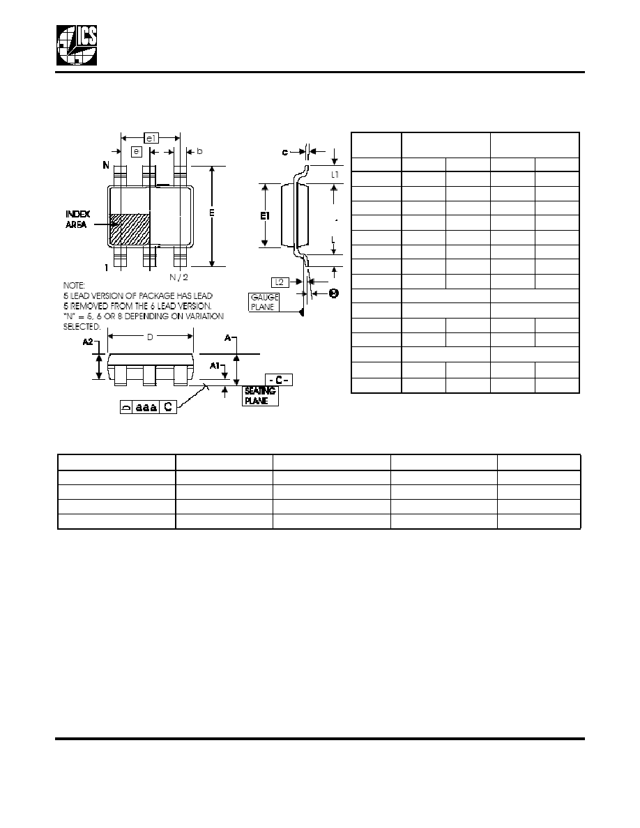
Package Outline and Package Dimensions
(6-pin TSOT-23-6)
Package dimensions are kept current with JEDEC Publication No. 95
Ordering Information
Parts that are ordered with a "LF" suffix to the part number are the Pb-Free configuration and are RoHS compliant.
While the information presented herein has been checked for both accuracy and reliability, Integrated Circuit Systems (ICS)
assumes no responsibility for either its use or for the infringement of any patents or other rights of third parties, which would
result from its use. No other circuits, patents, or licenses are implied. This product is intended for use in normal commercial
applications. Any other applications such as those requiring extended temperature range, high reliability, or other extraordinary
environmental requirements are not recommended without additional processing by ICS. ICS reserves the right to change any
circuitry or specifications without notice. ICS does not authorize or warrant any ICS product for use in life support devices or
critical medical instruments.
Part / Order Number
Marking
Shipping Packaging
Package
Temperature
ICS726T
726
Tubes
6-pin TSOT-23-6
0 to +70
∞ C
ICS726TT
726
Tape and Reel
6-pin TSOT-23-6
0 to +70
∞ C
ICS726TLF
726
Tubes
6-pin TSOT-23-6
0 to +70
∞ C
ICS726TLFT
726
Tape and Reel
6-pin TSOT-23-6
0 to +70
∞ C
Millimeters
Inches
Symbol
Min
Max
Min
Max
A
0.90
1.45
.0354
.0571
A1
0
0.15
0
.0059
A2
0.90
1.30
.0354
.0512
b
0.35
0.50
.0138
.0197
c
0.09
0.22
.0036
.0087
D
2.80
3.00
.1102
.1181
E
2.60
3.00
.1024
.1181
E1
1.50
1.75
.0591
.0689
e
0.95 BASIC
0.0374 BASIC
e1
1.90 BASIC
0.0748 BASIC
L
0.35
0.55
.0138
.0217
L1
0.50
0.70
.0197
.0276
L2
0.25 BASIC
.0098 BASIC
0
∞
10
∞
0
∞
10
∞
aaa
--
0.10
--
.0039