 | –≠–ª–µ–∫—Ç—Ä–æ–Ω–Ω—ã–π –∫–æ–º–ø–æ–Ω–µ–Ω—Ç: ICS728MLF | –°–∫–∞—á–∞—Ç—å:  PDF PDF  ZIP ZIP |

ICS728
MDS 728 B
1
Revision 012505
I n t e gr a t e d C i r c u i t S y s t e m s
l
5 2 5 R a c e S t r e e t , S a n J o s e, C A 9 5 1 2 6
l
t e l ( 4 0 8 ) 2 9 7 - 1 2 0 1
l
w w w. i c s t . c o m
L
OW
C
OST
27 MH
Z
3.3 V
OLT
VCXO
Description
The ICS728 combines the functions of a VCXO
(Voltage Controlled Crystal Oscillator) and PLL (Phase
Locked Loop) frequency doubler onto a single chip.
Used in conjunction with an external pullable quartz
crystal, this monolithic integrated circuit replaces more
costly hybrid (canned) VCXO devices. The ICS728 is
designed primarily for data and clock recovery
applications within end products such as set-top box
receivers.
The ICS728 exhibits a moderate VCXO gain of 110
ppm/V typical, when used with a high quality external
pullable quartz crystal.
The frequency of the on-chip VCXO is adjusted by an
external control voltage input into pin VIN. Because
VIN is a high impedance input, it can be driven directly
from an PWM RC integrator circuit. Frequency output
increases with VIN voltage input. The usable range of
VIN is 0 to 3.3 V.
Features
∑
Ideal for set-top box applications using 13.5 MHz
external pullable crystal to generate lock 27 MHz
clock transport video clock
∑
On-chip VCXO with guaranteed pull range of ±110
ppm minimum
∑
VCXO input tuning voltage 0 to 3.3 V
∑
Packaged in 8-pin SOIC (150 mil wide)
∑
Available in Pb (lead) free package
Block Diagram
27 MHz
(2x Crystal Frequency)
X1
X2
Voltage
Controlled
Crystal
Oscillator
PLL
Frequency
Doubler
VIN
13.5 MHz
Pullable
Crystal
L
OW
C
OST
27 MH
Z
3.3 V
OLT
VCXO
MDS 728 B
2
Revision 012505
I n t e gr a t e d C i r c u i t S y s t e m s
l
5 2 5 R a c e S t r e e t , S a n J o s e, C A 9 5 1 2 6
l
t e l ( 4 0 8 ) 2 9 7 - 1 2 0 1
l
w w w. i c s t . c o m
ICS728
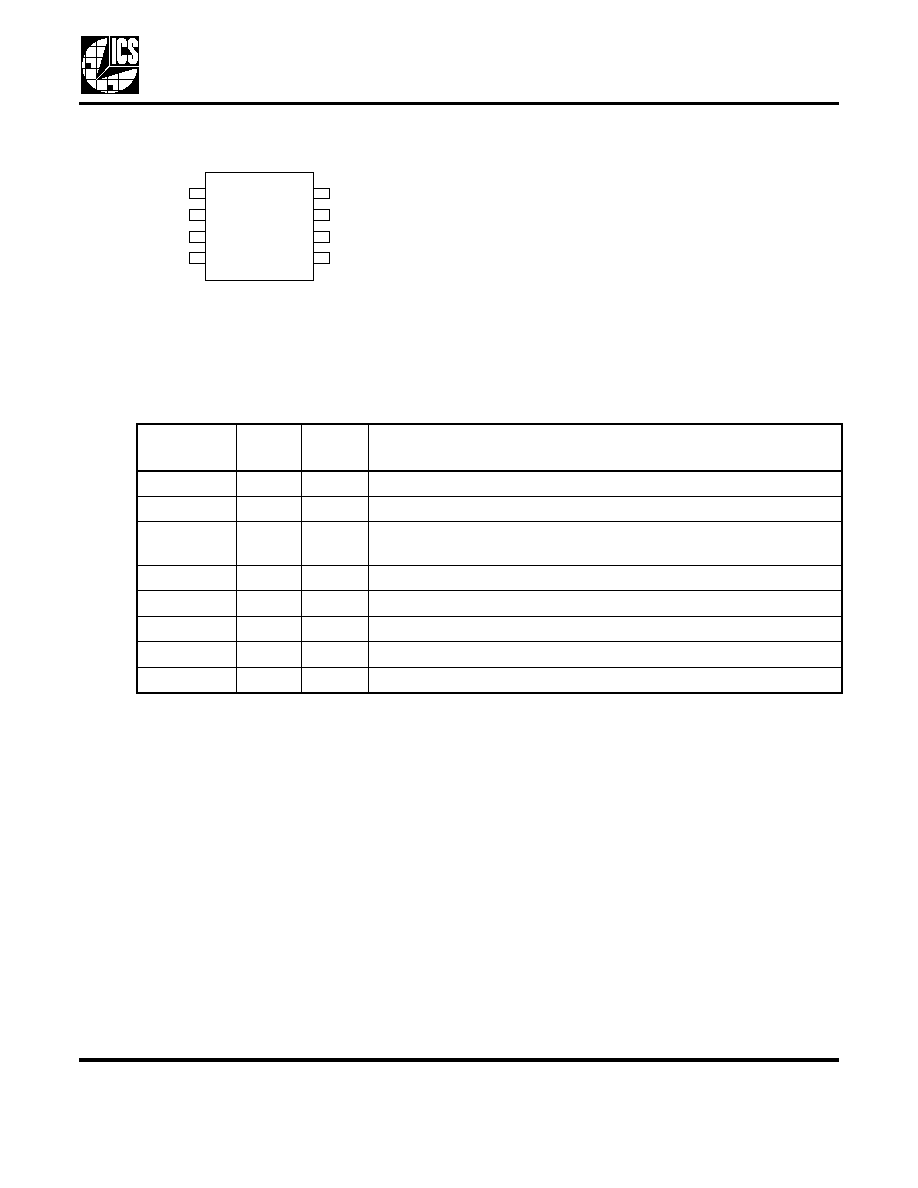
Pin Assignment
Pin Descriptions
X 1
VDD
V I N
GND
GND
CL K
DC
X 2
1
2
3
4
8
7
6
5
8 - pi n ( 1 50 mi l ) SOI C
Pin
Number
Pin
Name
Pin
Type
Pin Description
1
XI
Input
Crystal connection. Connect to the external pullable crystal.
2
VDD
Power
Connect to +3.3 V (0.01uf decoupling capacitor recommended).
3
VIN
Input
Voltage input to VCXO. Zero to 3.3 V analog input which controls the
oscillation frequency of the VCXO.
4
GND
Power
Connect to ground.
5
CLK
Output
Clock output.
6
DC
__
Do not connect to this pin
7
GND
Power
Connect to ground.
8
X2
Input
Crystal connection. Connect to the external pullable crystal.
L
OW
C
OST
27 MH
Z
3.3 V
OLT
VCXO
MDS 728 B
3
Revision 012505
I n t e gr a t e d C i r c u i t S y s t e m s
l
5 2 5 R a c e S t r e e t , S a n J o s e, C A 9 5 1 2 6
l
t e l ( 4 0 8 ) 2 9 7 - 1 2 0 1
l
w w w. i c s t . c o m
ICS728
External Component Selection
The ICS728 requires a minimum number of external
components for proper operation.
Decoupling Capacitor
A decoupling capacitor of 0.01µF must be connected
between VDD (pin 2) and GND (pin 4), as close to
these pins as possible. For optimum device
performance, the decoupling capacitor should be
mounted on the component side of the PCB. Avoid the
use of vias in the decoupling circuit.
Series Termination Resistor
When the PCB trace between the clock output (CLK,
pin 5) and the load is over 1 inch, series termination
should be used. To series terminate a 50
trace (a
commonly used trace impedance) place a 33
resistor
in series with the clock line, as close to the clock output
pin as possible. The nominal impedance of the clock
output is 20
.
Quartz Crystal
The ICS728 VCXO function consists of the external
crystal and the integrated VCXO oscillator circuit. To
assure the best system performance (frequency pull
range) and reliability, a crystal device with the
recommended parameters (shown below) must be
used, and the layout guidelines discussed in the
following section shown must be followed.
The frequency of oscillation of a quartz crystal is
determined by its "cut" and by the load capacitors
connected to it. The ICS728 incorporates on-chip
variable load capacitors that "pull" (change) the
frequency of the crystal. The crystal specified for use
with the ICS728 is designed to have zero frequency
error when the total of on-chip + stray capacitance is 14
pF.
Recommended Crystal Parameters:
Initial Accuracy at 25
∞
C
±20 ppm
Temperature Stability
±30 ppm
Aging
±20 ppm
Load Capacitance
14 pf
Shunt Capacitance, C0
7 pF Max
C0/C1 Ratio
250 Max
Equivalent Series Resistance
35
Max
The third overtone mode of the crystal and all spurs
must be >100 ppm distant from 3x the fundamental
resonance measured with a physical load of 14 pF.
The external crystal must be connected as close to the
chip as possible and should be on the same side of the
PCB as the ICS728. There should be no vias between
the crystal pins and the X1 and X2 device pins. There
should be no signal traces underneath or close to the
crystal.
Crystal Tuning Load Capacitors
The crystal traces should include pads for small fixed
capacitors, one between X1 and ground, and another
between X2 and ground. Stuffing of these capacitors
on the PCB is optional. The need for these capacitors is
determined at system prototype evaluation, and is
influenced by the particular crystal used and by PCB
layout. The typical required capacitor value is 1 to 4 pF.
To determine the need for and value of the crystal
adjustment capacitors, you will need a PC board of
your final layout, a frequency counter capable of 1 ppm
resolution and accuracy, two power supplies, and some
samples of the crystals which you plan to use in
production, along with measured initial accuracy for
each crystal at the specified crystal load capacitance,
CL.
To determine the value of the crystal capacitors:
1. Connect VDD of the ICS728 to 3.3 V. Connect pin 3
of the ICS728 to the second power supply. Adjust the
voltage on pin 3 to 0V. Measure and record the
frequency of the CLK output.
2. Adjust the voltage on pin 3 to 3.3 V. Measure and
record the frequency of the same output.
To calculate the centering error:
Where:
f
target
= nominal crystal frequency
error
xtal
=actual initial accuracy (in ppm) of the crystal
being measured
If the centering error is less than ±25 ppm, no
adjustment is needed. If the centering error is more
than 25 ppm negative, the PC board has excessive
stray capacitance and a new PCB layout should be
considered to reduce stray capacitance. (Alternately,
the crystal may be re-specified to a higher load
Error
10
6
x
f
3.0V
f
t
et
arg
≠
(
)
f
0V
f
t
et
arg
≠
(
)
+
f
t
et
arg
------------------------------------------------------------------------------
error
xtal
≠
=

L
OW
C
OST
27 MH
Z
3.3 V
OLT
VCXO
MDS 728 B
4
Revision 012505
I n t e gr a t e d C i r c u i t S y s t e m s
l
5 2 5 R a c e S t r e e t , S a n J o s e, C A 9 5 1 2 6
l
t e l ( 4 0 8 ) 2 9 7 - 1 2 0 1
l
w w w. i c s t . c o m
ICS728
capacitance. Contact ICS for details.) If the centering
error is more than 25 ppm positive, add identical fixed
centering capacitors from each crystal pin to ground.
The value for each of these caps (in pF) is given by:
External Capacitor = 2 x (centering error)/(trim
sensitivity)
Trim sensitivity is a parameter which can be supplied by
your crystal vendor. If you do not know the value,
assume it is 30 ppm/pF. After any changes, repeat the
measurement to verify that the remaining error is
acceptably low (typically less than ±25 ppm).
Absolute Maximum Ratings
Stresses above the ratings listed below can cause permanent damage to the ICS728. These ratings, which
are standard values for ICS commercially rated parts, are stress ratings only. Functional operation of the
device at these or any other conditions above those indicated in the operational sections of the
specifications is not implied. Exposure to absolute maximum rating conditions for extended periods can
affect product reliability. Electrical parameters are guaranteed only over the recommended operating
temperature range.
Recommended Operation Conditions
Item
Rating
Supply Voltage, VDD
7 V
All Inputs and Outputs
-0.5 V to VDD+0.5 V
Storage Temperature
-65 to +150
∞C
Soldering Temperature
260
∞C
Parameter
Min.
Typ.
Max.
Units
Ambient Operating Temperature
0
+70
∞C
Power Supply Voltage (measured in respect to GND)
+3.15
+3.45
V
Reference crystal parameters
Refer to page 3

L
OW
C
OST
27 MH
Z
3.3 V
OLT
VCXO
MDS 728 B
5
Revision 012505
I n t e gr a t e d C i r c u i t S y s t e m s
l
5 2 5 R a c e S t r e e t , S a n J o s e, C A 9 5 1 2 6
l
t e l ( 4 0 8 ) 2 9 7 - 1 2 0 1
l
w w w. i c s t . c o m
ICS728
DC Electrical Characteristics
VDD=3.3 V ±5%
, Ambient temperature 0 to +70
∞C, unless stated otherwise
AC Electrical Characteristics
VDD = 3.3 V ±5%, Ambient Temperature 0 to +70
∞ C, unless stated otherwise
Note 1: External crystal device must conform with Pullable Crystal Specifications listed on page 3.
Thermal Characteristics
Parameter
Symbol
Conditions
Min.
Typ.
Max.
Units
Operating Voltage
VDD
3.15
3.45
V
Output High Voltage
V
OH
I
OH
= -12 mA
2.4
V
Output Low Voltage
V
OL
I
OL
= 12 mA
0.4
V
Output High Voltage (CMOS
Level)
V
OH
I
OH
= -4 mA
VDD-0.4
V
Operating Supply Current
IDD
Output = 27 MHz,
no load
12
mA
Short Circuit Current
I
OS
±50
mA
VIN, VCXO Control Voltage
V
IA
0
3.3
V
Parameter
Symbol
Conditions
Min.
Typ.
Max.
Units
Output Frequency
F
O
27
MHz
Crystal Pullability
F
P
0V< VIN < 3.3 V, Note 1
+ 110
ppm
VCXO Gain
VIN = VDD/2 +1 V, Note 1
120
ppm/V
Output Rise Time
t
OR
0.8 to 2.0 V, C
L
=15 pF
1.5
ns
Output Fall Time
t
OF
2.0 to 0.8 V, C
L
=15 pF
1.5
ns
Output Clock Duty Cycle
t
D
Measured at 1.4 V, C
L
=15 pF
40
50
60
%
Maximum Output Jitter,
short term
t
J
C
L
=15 pF
100
ps
Parameter
Symbol
Conditions
Min.
Typ.
Max.
Units
Thermal Resistance Junction to
Ambient
JA
Still air
150
∞C/W
JA
1 m/s air flow
140
∞C/W
JA
3 m/s air flow
120
∞C/W
Thermal Resistance Junction to Case
JC
40
∞C/W

L
OW
C
OST
27 MH
Z
3.3 V
OLT
VCXO
MDS 728 B
6
Revision 012505
I n t e gr a t e d C i r c u i t S y s t e m s
l
5 2 5 R a c e S t r e e t , S a n J o s e, C A 9 5 1 2 6
l
t e l ( 4 0 8 ) 2 9 7 - 1 2 0 1
l
w w w. i c s t . c o m
ICS728
Marking Diagram
Marking Diagram (Pb free)
Notes:
1. ###### is the lot number.
2. YYWW is the last two digits of the year and week that the part was assembled.
3. "LF" denotes Pb (lead) free package.
4. Bottom marking: (origin)
Origin = country of origin of not USA.
ICS728M
######
YYWW$$
1
4
5
8
728MLF
######
YYWW
1
4
5
8
L
OW
C
OST
27 MH
Z
3.3 V
OLT
VCXO
MDS 728 B
7
Revision 012505
I n t e gr a t e d C i r c u i t S y s t e m s
l
5 2 5 R a c e S t r e e t , S a n J o s e, C A 9 5 1 2 6
l
t e l ( 4 0 8 ) 2 9 7 - 1 2 0 1
l
w w w. i c s t . c o m
ICS728
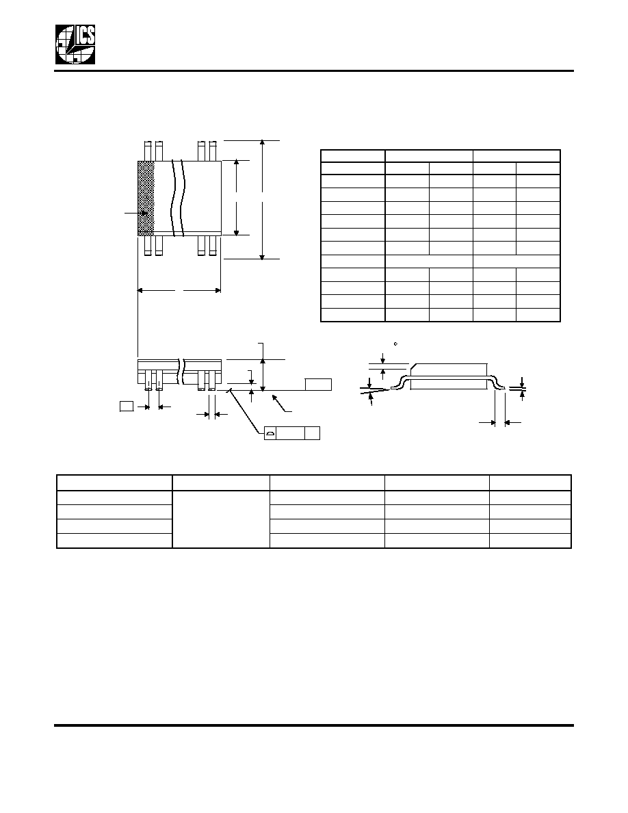
Package Outline and Package Dimensions (8-pin SOIC, 150 Mil. Narrow Body)
Package dimensions are kept current with JEDEC Publication No. 95
Ordering Information
Parts that are ordered with a "LF" suffix to the part number are the Pb-Free configuration and are RoHS compliant.
While the information presented herein has been checked for both accuracy and reliability, Integrated Circuit Systems (ICS)
assumes no responsibility for either its use or for the infringement of any patents or other rights of third parties, which would
result from its use. No other circuits, patents, or licenses are implied. This product is intended for use in normal commercial
applications. Any other applications such as those requiring extended temperature range, high reliability, or other extraordinary
environmental requirements are not recommended without additional processing by ICS. ICS reserves the right to change any
circuitry or specifications without notice. ICS does not authorize or warrant any ICS product for use in life support devices or
critical medical instruments.
Part / Order Number
Marking
Shipping Packaging
Package
Temperature
ICS728M
see page 6
Tubes
8-pin SOIC
0 to +70
∞ C
ICS728MT
Tape and Reel
8-pin SOIC
0 to +70
∞ C
ICS728MLF
Tubes
8-pin SOIC
0 to +70
∞ C
ICS728MLFT
Tape and Reel
8-pin SOIC
0 to +70
∞ C
INDEX
AREA
1 2
8
D
E
SEATING
PLANE
A1
A
e
- C -
B
.10 (.004)
C
C
L
H
h x 45
Millimeters
Inches
Symbol
Min
Max
Min
Max
A
1.35
1.75
0.0532
0.0688
A1
1.10
0.25
0.0040
0.0098
B
0.33
0.51
0.013
0.020
C
0.19
0.25
0.0075
0.0098
D
4.80
5.00
.1890
.1968
E
3.80
4.00
0.1497
0.1574
e
1.27 Basic
0.050 Basic
H
5.80
6.20
0.2284
0.2440
h
0.25
0.50
0.010
0.020
L
0.40
1.27
0.016
0.050
a
0
∞
8
∞
0
∞
8
∞

L
OW
C
OST
27 MH
Z
3.3 V
OLT
VCXO
MDS 728 B
8
Revision 012505
I n t e gr a t e d C i r c u i t S y s t e ms
l
5 2 5 R a c e S t r e e t , S a n J o s e, C A 9 5 1 2 6
l
t e l ( 4 0 8 ) 2 9 7 - 1 2 0 1
l
w w w. i c s t . c o m
ICS728
Revision History
Rev.
Originator
Date
Description of Change
A
J. Sarma
12/14/04
Release from Prelim to Final; release as General purpose device.
B
J. Sarma
01/25/05
Add marking diagrams; add LF.