Document Outline
- General Description
- Features
- Output Rates Supported
- Example Frequency Conversions
- Pin Assignment
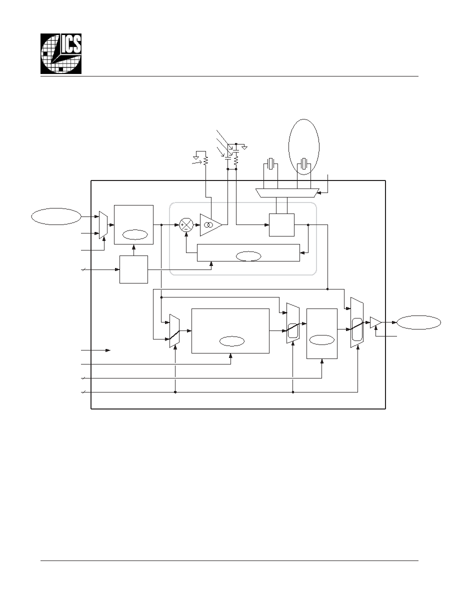
- Block Diagram
- Pin Descriptions
- Pin Characteristics
- First Frequency Translation Stage: VCXO PLL
- Second Frequency Translation Stage: FemtoClock Multiplier
- Bypass Function Table
- Example Frequency Configuration Table
- Example Frequency Configuration Table continued
- Absolute Maximum Ratings
- Power Supply DC Characteristics
- LVCMOS DC Characteristics
- Crystal Characteristics
- AC Characteristics
- Typical Phase Noise Plot
- Parameter Measurement Information
- Application Information
- Example Loop Filter Component Values
- Application Example 1
- Application Example 2
- Description of the PLL Stages
- VCXO PLL Loop Response Considerations
- Setting the VCXO PLL Loop Response
- External VCXO PLL Components
- Notes on Setting the Value of CP
- Notes on External Crystal Load Capacitors
- Loop Filter Response Software
- VCXO Crystal Selection
- VCXO Oscillator Circuit Example
- Crystal Parameter Examples
- Varactor Parameters
- Formulas
- Example Calculations
- Notes on Setting Charge Pump Current
- Charge Pump Current Example Seetings
- Charge Pump Current vs Value of RSET Graph
- Power Supply Filtering Techniques
- Reliability Information
- Transistor Count
- Package Outline
- Package Dimensions
- Ordering Information

810001BK-21
www.icst.com/products/hiperclocks.html
REV. A AUGUST 12, 2005
1
Integrated
Circuit
Systems, Inc.
ICS810001-21
F
EMTO
C
LOCKS
TM D
UAL
VCXO V
IDEO
PLL
PRELIMINARY
G
ENERAL
D
ESCRIPTION
T h e I C S 8 1 0 0 0 1 - 2 1 i s a m e m b e r o f t h e
HiperClockSTM family of high performance clock
solutions from ICS. The ICS810001-21 is a PLL
based synchronous clock generator that is
optimized for digital video clock jitter attenuation
and frequency translation. The device contains two internal
frequency multiplication stages that are cascaded in series.
The first stage is a VCXO PLL that is optimized to provide
reference clock jitter attenuation, and to support the complex
PLL multiplication ratios needed for video rate conversion.
The second stage is a FemtoClock frequency multiplier that
provides the low jitter, high frequency video output clock.
Preset multiplication ratios are selected from internal lookup
tables using device input selection pins. The multiplication ra-
tios are optimized to support most common video rates used in
professional video system applications. The VCXO requires
the use of an external, inexpensive pullable crystal. Two crys-
tal connections are provided (pin selectable) so that both 60
and 59.94 base frame rates can be supported. The VCXO re-
quires external passive loop filter components which are used
to set the PLL loop bandwidth and damping characteristics.
P
IN
A
SSIGNMENT
HiPerClockSTM
ICS
F
EATURES
∑ Accepts various HD and SD references including hsync,
transport and pixel clock rates
∑ Outputs HD and SD pixel rates
∑ One LVCMOS/LVTTL PLL clock output
∑ Two selectable LVCMOS/LVTTL input clocks
∑ LVCMOS input select lines
∑ VCXO PLL bandwidth can be optimized for jitter attenuation
and reference tracking
∑ FemtoClock frequency multiplier provides low jitter, high
frequency output
∑ FemtoClock range: 560MHz - 700MHz
∑ RMS phase jitter @148.3516484MHz, using a
26.973027MHz crystal (12kHz - 20MHz): 0.81ps (typical)
∑ 3.3V supply voltage
∑ 0∞C to 70∞C ambient operating temperature
32 31 30 29 28 27 26 25
9 1 0 1 1 1 2 1 3 1 4 1 5 1 6
1
2
3
4
5
6
7
8
24
23
22
21
20
19
18
17
N 0
N 1
nBP1
OE
GND
Q
V
DDO
V
DDA
ICS810001-21
CLK0
V0
V
DD
MR
MF
V1
V2
V3
V
DD
XT
AL_SEL
X
T
AL_OUT1
XT
AL_IN1
GND
X
T
AL_OUT0
XT
AL_IN0
V
DDX
LF1
LF0
ISET
V
DD
nBP0
GND
CLK_SEL
CLK1
32-Lead VFQFN
5mm x 5mm x 0.95 package body
K Package
Top View
O
UTPUT
R
ATES
S
UPPORTED
:
)
z
H
M
(
y
c
n
e
u
q
e
r
F
n
o
i
t
a
c
i
l
p
p
A
z
H
M
7
2
6
5
6
R
I
C
C
,
1
0
6
R
-
U
T
I
,
t
r
o
p
s
n
a
r
T
G
E
P
M
z
H
M
7
2
0
3
7
9
.
6
2
1
0
0
1
/
0
0
0
1
x
z
H
M
7
2
z
H
M
5
2
.
4
7
0
6
/
M
2
9
2
E
T
P
M
S
z
H
M
8
1
4
2
8
5
7
1
.
4
7
4
9
.
9
5
/
M
2
9
2
E
T
P
M
S
z
H
M
5
.
8
4
1
P
0
8
0
1
,
0
6
/
M
2
9
2
E
T
P
M
S
z
H
M
4
8
4
6
1
5
3
.
8
4
1
P
0
8
0
1
,
4
9
.
9
5
/
M
2
9
2
E
T
P
M
S
z
H
M
6
3
"
D
"
l
e
v
e
L
M
9
5
2
E
T
P
M
S
E
XAMPLE
F
REQUENCY
C
ONVERSIONS
:
All nine combinations from / to:
27MHz
74.175MHz
74.25MHz
NTSC or PAL hsync to 27MHz
NTSC or PAL hsync to 4xFsc
The Preliminary Information presented herein represents a product in prototyping or pre-production. The noted characteristics are based on initial
product characterization. Integrated Circuit Systems, Incorporated (ICS) reserves the right to change any circuitry or specifications without notice.
810001BK-21
www.icst.com/products/hiperclocks.html
REV. A AUGUST 12, 2005
2
Integrated
Circuit
Systems, Inc.
ICS810001-21
F
EMTO
C
LOCKS
TM D
UAL
VCXO V
IDEO
PLL
PRELIMINARY
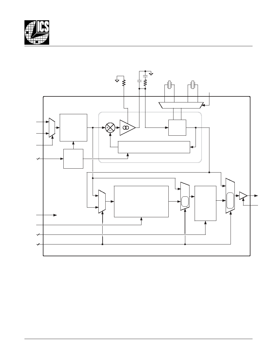
B
LOCK
D
IAGRAM
Charge
Pump
VCXO
V3:V0
Phase
Detector
Q
Output
Divider
00 = 4
01 = 8
10 = 12
11 = 18
VCXO Feedback Divider
(M Value from Table)
VCXO Input
Pre-Divider
(P Value
from Table)
VCXO Jitter Attenuation PLL
XT
AL_IN0
XT
AL_OUT0
XT
AL_IN1
XT
AL_OUT1
LF1
LF0
ISET
Loop
Filter
VCXO
Divider
Table
OE
XT
AL_SEL
0
1
MF
MR
Master Reset
0
1
CLK0
CLK1
CLK_SEL
N1:N0
4
2
11
10
10
11
01
01
10
11
00
2
nBP1:nBP0
FemtoClock
Frequency Multiplier
0= x22
1= x24
810001BK-21
www.icst.com/products/hiperclocks.html
REV. A AUGUST 12, 2005
3
Integrated
Circuit
Systems, Inc.
ICS810001-21
F
EMTO
C
LOCKS
TM D
UAL
VCXO V
IDEO
PLL
PRELIMINARY
T
ABLE
2. P
IN
C
HARACTERISTICS
l
o
b
m
y
S
r
e
t
e
m
a
r
a
P
s
n
o
i
t
i
d
n
o
C
t
s
e
T
m
u
m
i
n
i
M
l
a
c
i
p
y
T
m
u
m
i
x
a
M
s
t
i
n
U
C
N
I
e
c
n
a
t
i
c
a
p
a
C
t
u
p
n
I
4
F
p
C
D
P
e
c
n
a
t
i
c
a
p
a
C
n
o
i
t
a
p
i
s
s
i
D
r
e
w
o
P
)
t
u
p
t
u
o
r
e
p
(
V
D
D
V
,
A
D
D
V
,
O
D
D
V
5
6
4
.
3
=
D
B
T
F
p
R
P
U
L
L
U
P
r
o
t
s
i
s
e
R
p
u
ll
u
P
t
u
p
n
I
1
5
k
R
N
W
O
D
L
L
U
P
r
o
t
s
i
s
e
R
n
w
o
d
ll
u
P
t
u
p
n
I
1
5
k
T
ABLE
1. P
IN
D
ESCRIPTIONS
r
e
b
m
u
N
e
m
a
N
e
p
y
T
n
o
i
t
p
i
r
c
s
e
D
2
,
1
0
F
L
,
1
F
L
g
o
l
a
n
A
t
u
p
t
u
O
/
t
u
p
n
I
.
s
n
i
p
e
d
o
n
n
o
i
t
c
e
n
n
o
c
r
e
t
li
f
p
o
o
L
3
T
E
S
I
g
o
l
a
n
A
t
u
p
t
u
O
/
t
u
p
n
I
.
n
i
p
g
n
i
t
t
e
s
t
n
e
r
r
u
c
p
m
u
p
e
g
r
a
h
C
5
2
,
1
1
,
4
V
D
D
r
e
w
o
P
.
s
n
i
p
y
l
p
p
u
s
r
e
w
o
p
e
r
o
C
2
2
,
5
,
0
P
B
n
1
P
B
n
t
u
p
n
I
p
u
ll
u
P
.
m
a
r
g
a
i
d
k
c
o
l
b
e
e
S
.
s
n
i
p
l
o
r
t
n
o
c
s
s
a
p
y
B
L
L
P
9
2
,
0
2
,
6
D
N
G
r
e
w
o
P
.
d
n
u
o
r
g
y
l
p
p
u
s
r
e
w
o
P
7
L
E
S
_
K
L
C
t
u
p
n
I
n
w
o
d
ll
u
P
s
t
c
e
l
e
s
,
W
O
L
n
e
h
W
.
1
K
L
C
s
t
c
e
l
e
s
H
G
I
H
n
e
h
W
.
t
c
e
l
e
s
k
c
o
l
c
t
u
p
n
I
.
s
l
e
v
e
l
e
c
a
f
r
e
t
n
i
L
T
T
V
L
/
S
O
M
C
V
L
.
0
K
L
C
9
,
8
0
K
L
C
,
1
K
L
C
t
u
p
n
I
n
w
o
d
ll
u
P
.
s
l
e
v
e
l
e
c
a
f
r
e
t
n
i
L
T
T
V
L
/
S
O
M
C
V
L
.
s
t
u
p
n
i
k
c
o
l
C
,
4
1
,
0
1
6
1
,
5
1
,
1
V
,
0
V
3
V
,
2
V
t
u
p
n
I
n
w
o
d
ll
u
P
.
s
l
e
v
e
l
e
c
a
f
r
e
t
n
i
L
T
T
V
L
/
S
O
M
C
V
L
.
s
n
i
p
n
o
i
t
c
e
l
e
s
r
e
d
i
v
i
d
L
L
P
O
X
C
V
2
1
R
M
t
u
p
n
I
n
w
o
d
ll
u
P
s
r
e
d
i
v
i
d
l
a
n
r
e
t
n
i
e
h
t
,
H
G
I
H
c
i
g
o
l
n
e
h
W
.
t
e
s
e
R
r
e
t
s
a
M
H
G
I
H
e
v
i
t
c
A
e
h
t
,
W
O
L
c
i
g
o
l
n
e
h
W
.
w
o
l
o
g
o
t
t
u
p
t
u
o
e
h
t
g
n
i
s
u
a
c
t
e
s
e
r
e
r
a
.
d
e
l
b
a
n
e
s
i
t
u
p
t
u
o
e
h
t
d
n
a
s
r
e
d
i
v
i
d
l
a
n
r
e
t
n
i
.
s
l
e
v
e
l
e
c
a
f
r
e
t
n
i
L
T
T
V
L
/
S
O
M
C
V
L
3
1
F
M
t
u
p
n
I
n
w
o
d
ll
u
P
.
n
i
p
t
c
e
l
e
s
r
o
t
c
a
f
n
o
i
t
a
c
il
p
i
t
l
u
m
k
c
o
l
C
o
t
m
e
F
.
s
l
e
v
e
l
e
c
a
f
r
e
t
n
i
L
T
T
V
L
/
S
O
M
C
V
L
7
1
V
A
D
D
r
e
w
o
P
.
n
i
p
y
l
p
p
u
s
g
o
l
a
n
A
8
1
V
O
D
D
r
e
w
o
P
.
n
i
p
y
l
p
p
u
s
r
e
w
o
p
t
u
p
t
u
O
9
1
Q
t
u
p
t
u
O
.
s
l
e
v
e
l
e
c
a
f
r
e
t
n
i
L
T
T
V
L
/
S
O
M
C
V
L
.
t
u
p
t
u
o
k
c
o
l
c
L
L
P
O
X
C
V
1
2
E
O
t
u
p
n
I
p
u
ll
u
P
.
e
t
a
t
s
i
r
t
n
i
s
i
t
u
p
t
u
o
k
c
o
l
c
e
h
t
,
W
O
L
c
i
g
o
l
n
e
h
W
.
e
l
b
a
n
e
t
u
p
t
u
O
.
d
e
l
b
a
n
e
s
i
t
u
p
t
u
o
e
h
t
,
H
G
I
H
c
i
g
o
l
n
e
h
W
.
s
l
e
v
e
l
e
c
a
f
r
e
t
n
i
L
T
T
V
L
/
S
O
M
C
V
L
4
2
,
3
2
0
N
,
1
N
t
u
p
n
I
n
w
o
d
ll
u
P
.
s
l
e
v
e
l
e
c
a
f
r
e
t
n
i
L
T
T
V
L
/
S
O
M
C
V
L
.
t
c
e
l
e
s
e
d
i
v
i
d
t
u
p
t
u
o
k
c
o
l
C
o
t
m
e
F
6
2
L
E
S
_
L
A
T
X
t
u
p
n
I
n
w
o
d
ll
u
P
s
t
c
e
l
e
s
,
W
O
L
n
e
h
W
.
1
L
A
T
X
s
t
c
e
l
e
s
,
H
G
I
H
n
e
h
W
.
t
c
e
l
e
s
l
a
t
s
y
r
C
.
s
l
e
v
e
l
e
c
a
f
r
e
t
n
i
L
T
T
V
L
/
S
O
M
C
V
L
.
0
L
A
T
X
,
7
2
8
2
,
1
T
U
O
_
L
A
T
X
1
N
I
_
L
A
T
X
t
u
p
n
I
.
t
u
p
n
i
e
h
t
s
i
1
N
I
_
L
A
T
X
.
e
c
a
f
r
e
t
n
i
r
o
t
a
ll
i
c
s
o
l
a
t
s
y
r
C
.
t
u
p
t
u
o
e
h
t
s
i
1
T
U
O
_
L
A
T
X
,
0
3
1
3
,
0
T
U
O
_
L
A
T
X
0
N
I
_
L
A
T
X
t
u
p
n
I
.
t
u
p
n
i
e
h
t
s
i
0
N
I
_
L
A
T
X
.
e
c
a
f
r
e
t
n
i
r
o
t
a
ll
i
c
s
o
l
a
t
s
y
r
C
.
t
u
p
t
u
o
e
h
t
s
i
0
T
U
O
_
L
A
T
X
2
3
V
X
D
D
r
e
w
o
P
.
p
m
u
p
e
g
r
a
h
c
O
X
C
V
r
o
f
n
i
p
y
l
p
p
u
s
r
e
w
o
P
:
E
T
O
N
p
u
ll
u
P
d
n
a
n
w
o
d
ll
u
P
.
s
e
u
l
a
v
l
a
c
i
p
y
t
r
o
f
,
s
c
i
t
s
i
r
e
t
c
a
r
a
h
C
n
i
P
,
2
e
l
b
a
T
e
e
S
.
s
r
o
t
s
i
s
e
r
t
u
p
n
i
l
a
n
r
e
t
n
i
o
t
r
e
f
e
r
810001BK-21
www.icst.com/products/hiperclocks.html
REV. A AUGUST 12, 2005
4
Integrated
Circuit
Systems, Inc.
ICS810001-21
F
EMTO
C
LOCKS
TM D
UAL
VCXO V
IDEO
PLL
PRELIMINARY
e
l
b
a
T
p
U
-
k
o
o
L
r
e
d
i
v
i
D
L
L
P
O
X
C
V
n
o
i
t
a
c
i
l
p
p
A
k
c
o
l
C
o
e
d
i
V
n
o
i
t
a
c
i
l
p
p
A
k
c
o
l
C
o
e
d
i
V
e
t
a
n
r
e
t
l
A
s
n
i
P
0
V
:
3
V
e
u
l
a
V
P
e
u
l
a
V
M
)
z
H
M
/
z
H
k
(
t
u
p
n
I
)
z
H
M
(
O
X
C
V
)
z
H
M
/
z
H
k
(
t
u
p
n
I
)
z
H
M
(
O
X
C
V
0
0
0
0
0
0
0
1
0
0
0
1
z
H
M
7
2
z
H
M
7
2
z
H
M
3
7
9
.
6
2
z
H
M
3
7
9
.
6
2
1
0
0
0
1
0
0
1
0
0
0
1
z
H
M
7
2
z
H
M
3
7
9
.
6
2
0
1
0
0
0
0
0
1
1
4
0
0
4
z
H
M
5
7
1
.
4
7
z
H
M
7
2
1
1
0
0
1
1
0
1
1
0
0
0
4
z
H
M
5
2
.
4
7
z
H
M
3
7
9
.
6
2
0
0
1
0
0
0
0
1
1
0
0
0
4
z
H
M
5
2
.
4
7
z
H
M
7
2
1
0
1
0
4
0
0
4
4
0
0
4
z
H
M
7
2
z
H
M
7
2
z
H
M
3
7
9
.
6
2
z
H
M
3
7
9
.
6
2
0
1
1
0
4
0
0
4
0
0
0
4
z
H
M
7
2
z
H
M
3
7
9
.
6
2
1
1
1
0
0
0
0
1
1
0
0
1
z
H
M
3
7
9
.
6
2
z
H
M
7
2
0
0
0
1
0
5
2
1
9
z
H
M
5
7
1
.
4
7
z
H
M
7
2
1
0
0
1
3
5
2
2
9
z
H
M
5
2
.
4
7
z
H
M
7
2
0
1
0
1
2
9
2
9
z
H
M
7
2
z
H
M
7
2
z
H
M
3
7
9
.
6
2
z
H
M
3
7
9
.
6
2
1
1
0
1
1
0
0
6
z
H
k
5
4
)
c
n
y
s
h
0
6
/
P
0
2
7
(
z
H
M
7
2
z
H
k
5
5
9
.
4
4
)
4
9
.
9
5
/
P
0
2
7
(
z
H
M
3
7
9
.
6
2
0
0
1
1
1
0
0
8
z
H
k
5
7
.
3
3
)
c
n
y
s
h
0
6
/
I
0
8
0
1
(
z
H
M
7
2
z
H
k
6
1
7
.
3
3
)
4
9
.
9
5
/
I
0
8
0
1
(
z
H
M
3
7
9
.
6
2
1
0
1
1
1
8
2
7
1
z
H
k
5
2
6
.
5
1
)
c
n
y
s
h
L
A
P
(
z
H
M
7
2
0
1
1
1
1
6
1
7
1
z
H
k
4
3
7
.
5
1
)
c
n
y
s
h
C
S
T
N
(
z
H
M
7
2
1
1
1
1
1
0
6
9
z
H
k
5
2
1
.
8
2
)
c
n
y
s
h
0
5
/
I
0
8
0
1
(
z
H
M
7
2
T
ABLE
3A. F
IRST
F
REQUENCY
T
RANSLATION
S
TAGE
: VCXO PLL
T
ABLE
3C. B
YPASS
F
UNCTION
T
ABLE
s
t
u
p
n
I
n
o
i
t
a
r
e
p
O
1
P
B
n
0
P
B
n
0
0
r
e
d
i
v
i
D
t
u
p
t
u
O
d
n
a
L
L
P
r
o
t
a
l
s
n
a
r
T
y
c
n
e
u
q
e
r
F
s
s
a
p
y
B
0
1
L
L
P
r
o
t
a
l
s
n
a
r
T
y
c
n
e
u
q
e
r
F
d
n
a
L
L
P
n
o
i
t
a
u
n
e
t
t
A
r
e
t
t
i
J
O
X
C
V
s
s
a
p
y
B
:
e
d
o
M
t
s
e
T
1
0
L
L
P
n
o
i
t
a
u
n
e
t
t
A
r
e
t
t
i
J
O
X
C
V
s
s
a
p
y
B
:
e
d
o
M
C
L
1
1
e
v
i
t
c
A
:
e
d
o
M
L
L
P
e
l
b
a
T
p
U
-
k
o
o
L
k
c
o
l
C
o
t
m
e
F
n
o
i
t
a
c
i
l
p
p
A
k
c
o
l
C
o
e
d
i
V
n
o
i
t
a
c
i
l
p
p
A
k
c
o
l
C
o
e
d
i
V
e
t
a
n
r
e
t
l
A
s
n
i
P
0
N
:
1
N
,
F
M
v
i
D
B
F
v
i
D
t
u
O
)
z
H
M
(
O
X
C
V
)
z
H
M
(
Q
)
z
H
M
(
O
X
C
V
)
z
H
M
(
Q
0
0
,
0
2
2
4
z
H
M
7
2
z
H
M
5
.
8
4
1
z
H
M
3
7
9
.
6
2
z
H
M
5
3
.
8
4
1
1
0
,
0
2
2
8
z
H
M
7
2
z
H
M
5
2
.
4
7
z
H
M
3
7
9
.
6
2
z
H
M
5
7
1
.
4
7
0
1
,
0
2
2
2
1
1
1
,
0
2
2
8
1
0
0
,
1
4
2
4
1
0
,
1
4
2
8
0
1
,
1
4
2
2
1
z
H
M
7
2
z
H
M
4
5
1
1
,
1
4
2
8
1
z
H
M
7
2
z
H
M
6
3
T
ABLE
3B. S
ECOND
F
REQUENCY
T
RANSLATION
S
TAGE
: F
EMTO
C
LOCK
M
ULTIPLIER
810001BK-21
www.icst.com/products/hiperclocks.html
REV. A AUGUST 12, 2005
5
Integrated
Circuit
Systems, Inc.
ICS810001-21
F
EMTO
C
LOCKS
TM D
UAL
VCXO V
IDEO
PLL
PRELIMINARY
T
ABLE
3D
.
E
XAMPLE
F
REQUENCY
C
ONFIGURA
TION
T
ABLE
,
CONTINUED
ON
NEXT
PA
G
E
n
o
i
t
a
r
u
g
i
f
n
o
C
e
l
p
m
a
x
E
r
e
b
m
u
N
t
u
p
n
I
e
c
n
e
r
e
f
e
R
y
c
n
e
u
q
e
r
F
)
z
H
M
(
e
c
n
e
r
e
f
e
R
k
c
o
l
C
n
o
i
t
p
i
r
c
s
e
D
L
L
P
O
X
C
VL
L
P
k
c
o
l
C
o
t
m
e
F
L
E
S
_
O
C
V
t
u
p
t
u
O
y
c
n
e
u
q
e
r
F
)
z
H
M
(n
o
i
t
p
i
r
c
s
e
D
t
u
p
t
u
O
P
t
u
p
n
I
r
e
d
i
v
i
D
M
k
c
a
b
d
e
e
F
r
e
d
i
v
i
D
L
A
T
X
y
c
n
e
u
q
e
r
F
)
z
H
M
(
F
M
k
c
a
b
d
e
e
F
r
e
d
i
v
i
D
N
t
u
p
t
u
O
r
e
d
i
v
i
D
17
2t
r
o
p
s
n
a
r
T1
0
0
10
0
0
17
2
0
3
7
9
.
6
22
28
1
8
1
4
2
8
5
7
1
.
4
74
9
.
9
5
/
M
2
9
2
E
T
P
M
S
27
2t
r
o
p
s
n
a
r
T0
0
0
10
0
0
17
22
28
1
5
2
.
4
70
6
/
M
2
9
2
E
T
P
M
S
37
2t
r
o
p
s
n
a
r
T1
0
0
10
0
0
17
2
0
3
7
9
.
6
22
24
1
4
8
4
6
1
5
3
.
8
4
1)
P
0
8
0
1
(
4
9
.
9
5
/
M
2
9
2
E
T
P
M
S
47
2t
r
o
p
s
n
a
r
T0
0
0
10
0
0
17
22
24
1
5
.
8
4
1)
P
0
8
0
1
(
0
6
/
M
2
9
2
E
T
P
M
S
57
2t
r
o
p
s
n
a
r
T1
0
0
10
0
0
17
2
0
3
7
9
.
6
2a
na
n0
7
2
0
3
7
9
.
6
21
0
0
1
/
0
0
0
1
x
t
r
o
p
s
n
a
r
T
67
2t
r
o
p
s
n
a
r
T0
0
0
10
0
0
17
2a
na
n0
7
2t
r
o
p
s
n
a
r
T
0
14
2
8
5
7
1
.
4
74
9
.
9
5
/
M
2
9
20
0
0
1
14
0
0
47
22
28
1
5
2
.
4
70
6
/
M
2
9
2
E
T
P
M
S
1
15
2
.
4
70
6
/
M
2
9
21
1
0
1
10
0
0
47
2
0
3
7
9
.
6
22
28
1
8
1
4
2
8
5
7
1
.
4
74
9
.
9
5
/
M
2
9
2
E
T
P
M
S
2
14
2
8
5
7
1
.
4
74
9
.
9
5
/
M
2
9
20
0
0
1
10
0
0
47
2
0
3
7
9
.
6
22
28
1
8
1
4
2
8
5
7
1
.
4
74
9
.
9
5
/
M
2
9
2
E
T
P
M
S
3
15
2
.
4
70
6
/
M
2
9
20
0
0
1
10
0
0
47
22
28
1
5
2
.
4
70
6
/
M
2
9
2
E
T
P
M
S
4
14
2
8
5
7
1
.
4
74
9
.
9
5
/
M
2
9
20
0
0
1
14
0
0
47
2a
na
n0
7
2t
r
o
p
s
n
a
r
T
5
15
2
.
4
70
6
/
M
2
9
20
0
0
1
10
0
0
47
2a
na
n0
7
2t
r
o
p
s
n
a
r
T
6
17
2t
r
o
p
s
n
a
r
T4
0
0
44
0
0
47
2a
na
n0
7
2t
r
o
p
s
n
a
r
T
7
17
2t
r
o
p
s
n
a
r
T4
0
0
40
0
0
47
2
0
3
7
9
.
6
22
28
1
8
1
4
2
8
5
7
1
.
4
74
9
.
9
5
/
M
2
9
2
E
T
P
M
S
8
17
2t
r
o
p
s
n
a
r
T4
0
0
44
0
0
47
22
28
1
5
2
.
4
7B
D
H
0
24
2
8
5
7
1
.
4
74
9
.
9
5
/
M
2
9
20
5
21
97
22
28
1
5
2
.
4
70
6
/
M
2
9
2
E
T
P
M
S
1
25
2
.
4
70
6
/
M
2
9
23
5
22
97
22
28
1
5
2
.
4
7)
P
0
8
0
1
(
0
6
/
M
2
9
2
E
T
P
M
S
2
24
2
8
5
7
1
.
4
74
9
.
9
5
/
M
2
9
23
5
22
97
2
0
3
7
9
.
6
22
28
1
8
1
4
2
8
5
7
1
.
4
74
9
.
9
5
/
M
2
9
2
E
T
P
M
S
3
27
2t
r
o
p
s
n
a
r
T2
92
97
22
28
1
5
2
.
4
70
6
/
M
2
9
2
E
T
P
M
S
0
34
2
8
5
7
1
.
4
74
9
.
9
5
/
M
2
9
20
5
21
97
2a
na
n0
7
2t
r
o
p
s
n
a
r
T
1
35
2
.
4
70
6
/
M
2
9
23
5
22
97
2a
na
n0
7
2t
r
o
p
s
n
a
r
T
2
35
2
.
4
70
6
/
M
2
9
21
1
0
1
10
0
0
47
2
0
3
7
9
.
6
2a
na
n0
7
2
0
3
7
9
.
6
21
0
0
1
/
0
0
0
1
x
t
r
o
p
s
n
a
r
T
3
34
2
8
5
7
1
.
4
74
9
.
9
5
/
M
2
9
23
5
22
97
2
0
3
7
9
.
6
2a
na
n0
7
2
0
3
7
9
.
6
21
0
0
1
/
0
0
0
1
x
t
r
o
p
s
n
a
r
T
0
47
2t
r
o
p
s
n
a
r
T2
92
97
24
22
11
4
5e
l
p
m
a
s
r
e
v
O
6
5
6
/
1
0
6
R
-
U
T
I
1
47
2t
r
o
p
s
n
a
r
T2
92
97
24
28
11
6
3e
l
p
m
a
s
r
e
v
O
"
D
"
l
e
v
e
L
M
9
5
2
2
47
2t
r
o
p
s
n
a
r
T4
0
0
44
0
0
47
24
28
11
6
3e
l
p
m
a
s
r
e
v
O
"
D
"
l
e
v
e
L
M
9
5
2

810001BK-21
www.icst.com/products/hiperclocks.html
REV. A AUGUST 12, 2005
6
Integrated
Circuit
Systems, Inc.
ICS810001-21
F
EMTO
C
LOCKS
TM D
UAL
VCXO V
IDEO
PLL
PRELIMINARY
T
ABLE
3D
.
E
XAMPLE
F
REQ
UENCY
C
ONFIGURA
TION
T
ABLE
n
o
i
t
a
r
u
g
i
f
n
o
C
e
l
p
m
a
x
E
r
e
b
m
u
N
t
u
p
n
I
e
c
n
e
r
e
f
e
R
y
c
n
e
u
q
e
r
F
)
z
H
M
(
e
c
n
e
r
e
f
e
R
k
c
o
l
C
n
o
i
t
p
i
r
c
s
e
D
L
L
P
O
X
C
VL
L
P
k
c
o
l
C
o
t
m
e
F
L
E
S
_
O
C
V
t
u
p
t
u
O
y
c
n
e
u
q
e
r
F
)
z
H
M
(n
o
i
t
p
i
r
c
s
e
D
k
c
o
l
C
t
u
p
t
u
O
P
t
u
p
n
I
r
e
d
i
v
i
D
M
k
c
a
b
d
e
e
F
r
e
d
i
v
i
D
L
A
T
X
y
c
n
e
u
q
e
r
F
)
z
H
M
(
C
F
k
c
a
b
d
e
e
F
r
e
d
i
v
i
D
N
t
u
p
t
u
O
r
e
d
i
v
i
D
0
51
F2
92
91
Fa
na
n0
1
Fz
H
M
0
3
o
t
5
1
=
1
F
0
65
2
6
5
1
0
.
0c
n
y
s
H
L
A
P1
5
3
1
15
3
7
.
7
1a
na
n0
5
3
7
.
7
1)
c
s
F
x
4
(
r
e
i
r
r
a
c
b
u
s
L
A
P
x
4
1
64
3
7
5
1
0
.
0c
n
y
s
H
C
S
T
N1
0
1
98
1
8
1
3
.
4
1a
na
n0
8
1
8
1
3
.
4
1)
c
s
F
x
4
(
r
e
i
r
r
a
c
b
u
s
C
S
T
N
x
4
2
65
2
6
5
1
0
.
0c
n
y
s
H
L
A
P1
8
2
7
17
2a
na
n0
7
2t
r
o
p
s
n
a
r
T
3
64
3
7
5
1
0
.
0c
n
y
s
H
C
S
T
N1
6
1
7
17
2a
na
n0
7
2t
r
o
p
s
n
a
r
T
4
65
2
6
5
1
0
.
0c
n
y
s
H
L
A
P1
8
2
7
17
24
22
11
4
5e
l
p
m
a
s
r
e
v
O
6
5
6
/
1
0
6
R
-
U
T
I
5
64
3
7
5
1
0
.
0c
n
y
s
H
C
S
T
N1
6
1
7
17
24
22
11
4
5e
l
p
m
a
s
r
e
v
O
6
5
6
/
1
0
6
R
-
U
T
I
810001BK-21
www.icst.com/products/hiperclocks.html
REV. A AUGUST 12, 2005
7
Integrated
Circuit
Systems, Inc.
ICS810001-21
F
EMTO
C
LOCKS
TM D
UAL
VCXO V
IDEO
PLL
PRELIMINARY
T
ABLE
4A. P
OWER
S
UPPLY
DC C
HARACTERISTICS
,
V
DD
= V
DDA
= V
DDO
= V
DDX
= 3.3V±5%, T
A
= 0∞C
TO
70∞C
T
ABLE
4B. LVCMOS / LVTTL DC C
HARACTERISTICS
,
V
DD
= V
DDA
= V
DDO
= V
DDX
= 3.3V±5%, T
A
= 0∞C
TO
70∞C
NOTE 1: Outputs terminated with 50
to V
DDO
/2.
A
BSOLUTE
M
AXIMUM
R
ATINGS
Supply Voltage, V
DD
4.6V
Inputs, V
I
-0.5V to V
DD
+ 0.5V
Outputs, V
O
-0.5V to V
DDO
+ 0.5V
Package Thermal Impedance,
JA
34.8∞C/W (0 lfpm)
Storage Temperature, T
STG
-65∞C to 150∞C
NOTE: Stresses beyond those listed under Absolute
Maximum Ratings may cause permanent damage to the
device. These ratings are stress specifications only. Functional
operation of product at these conditions or any conditions be-
yond those listed in the
DC Characteristics
or
AC Character-
istics
is not implied. Exposure to absolute maximum rating
conditions for extended periods may affect product reliability.
l
o
b
m
y
S
r
e
t
e
m
a
r
a
P
s
n
o
i
t
i
d
n
o
C
t
s
e
T
m
u
m
i
n
i
M
l
a
c
i
p
y
T
m
u
m
i
x
a
M
s
t
i
n
U
V
D
D
e
g
a
t
l
o
V
y
l
p
p
u
S
e
r
o
C
5
3
1
.
3
3
.
3
5
6
4
.
3
V
V
A
D
D
e
g
a
t
l
o
V
y
l
p
p
u
S
g
o
l
a
n
A
5
3
1
.
3
3
.
3
5
6
4
.
3
V
V
O
D
D
e
g
a
t
l
o
V
y
l
p
p
u
S
t
u
p
t
u
O
5
3
1
.
3
3
.
3
5
6
4
.
3
V
V
X
D
D
e
g
a
t
l
o
V
y
l
p
p
u
S
p
m
u
P
e
g
r
a
h
C
5
3
1
.
3
3
.
3
5
6
4
.
3
V
I
D
D
t
n
e
r
r
u
C
y
l
p
p
u
S
r
e
w
o
P
0
1
2
A
m
I
A
D
D
t
n
e
r
r
u
C
y
l
p
p
u
S
g
o
l
a
n
A
0
1
A
m
I
O
D
D
t
n
e
r
r
u
C
y
l
p
p
u
S
t
u
p
t
u
O
5
A
m
I
X
D
D
t
n
e
r
r
u
C
y
l
p
p
u
S
p
m
u
P
e
g
r
a
h
C
D
B
T
A
m
l
o
b
m
y
S
r
e
t
e
m
a
r
a
P
s
n
o
i
t
i
d
n
o
C
t
s
e
T
m
u
m
i
n
i
M
l
a
c
i
p
y
T
m
u
m
i
x
a
M
s
t
i
n
U
V
H
I
t
u
p
n
I
e
g
a
t
l
o
V
h
g
i
H
0
.
3
V
D
D
3
.
0
+
V
V
L
I
e
g
a
t
l
o
V
w
o
L
t
u
p
n
I
3
.
0
-
8
.
0
V
I
H
I
t
u
p
n
I
t
n
e
r
r
u
C
h
g
i
H
,
F
M
,
R
M
,
1
K
L
C
,
0
K
L
C
,
0
:
1
N
,
0
:
3
V
,
0
P
:
1
P
L
E
S
_
L
A
T
X
,
L
E
S
_
K
L
C
V
D
D
V
=
N
I
V
5
6
4
.
3
=
0
5
1
A
µ
1
P
B
n
,
0
P
B
n
,
E
O
V
D
D
V
=
N
I
V
5
6
4
.
3
=
5
A
µ
I
L
I
t
u
p
n
I
t
n
e
r
r
u
C
w
o
L
,
F
M
,
R
M
,
1
K
L
C
,
0
K
L
C
,
0
:
1
N
,
0
:
3
V
,
0
P
:
1
P
L
E
S
_
L
A
T
X
,
L
E
S
_
K
L
C
V
D
D
V
,
V
5
6
4
.
3
=
N
I
V
0
=
5
-
A
µ
1
P
B
n
,
0
P
B
n
,
E
O
V
D
D
V
,
V
5
6
4
.
3
=
N
I
V
0
=
0
5
1
-
A
µ
V
H
O
1
E
T
O
N
;
e
g
a
t
l
o
V
h
g
i
H
t
u
p
t
u
O
6
.
2
V
V
L
O
1
E
T
O
N
;
e
g
a
t
l
o
V
w
o
L
t
u
p
t
u
O
5
.
0
V
810001BK-21
www.icst.com/products/hiperclocks.html
REV. A AUGUST 12, 2005
8
Integrated
Circuit
Systems, Inc.
ICS810001-21
F
EMTO
C
LOCKS
TM D
UAL
VCXO V
IDEO
PLL
PRELIMINARY
T
ABLE
5. C
RYSTAL
C
HARACTERISTICS
r
e
t
e
m
a
r
a
P
s
n
o
i
t
i
d
n
o
C
t
s
e
T
m
u
m
i
n
i
M
l
a
c
i
p
y
T
m
u
m
i
x
a
M
s
t
i
n
U
n
o
i
t
a
ll
i
c
s
O
f
o
e
d
o
M
l
a
t
n
e
m
a
d
n
u
F
y
c
n
e
u
q
e
r
F
4
1
5
3
z
H
M
)
R
S
E
(
e
c
n
a
t
s
i
s
e
R
s
e
i
r
e
S
t
n
e
l
a
v
i
u
q
E
0
5
e
c
n
a
t
i
c
a
p
a
C
t
n
u
h
S
7
F
p
K
O
X
C
V
O
C
V
K
(
O
X
C
V
1
E
T
O
N
;
)
0
0
0
7
V
/
z
H
F
(
e
g
n
a
R
ll
u
P
y
c
n
e
u
q
e
r
F
P
1
E
T
O
N
;
)
0
0
1
m
p
p
l
e
v
e
L
e
v
i
r
D
1
W
m
.
e
c
i
v
e
d
l
a
t
s
y
r
c
z
t
r
a
u
q
d
e
d
n
e
m
m
o
c
e
r
S
C
I
n
a
g
n
i
s
u
n
e
h
w
d
e
e
t
n
a
r
a
u
g
y
l
n
o
e
r
a
s
r
e
t
e
m
a
r
a
p
e
s
e
h
T
:
1
E
T
O
N
.
s
n
o
i
t
a
d
n
e
m
m
o
c
e
r
e
c
i
v
e
d
l
a
t
s
y
r
c
z
t
r
a
u
q
g
n
i
d
r
a
g
e
r
S
C
I
t
c
a
t
n
o
C
T
ABLE
6. AC C
HARACTERISTICS
,
V
DD
= V
DDA
= V
DDO
= V
DDX
= 3.3V±5%, T
A
= 0∞C
TO
70∞C
l
o
b
m
y
S
r
e
t
e
m
a
r
a
P
s
n
o
i
t
i
d
n
o
C
t
s
e
T
m
u
m
i
n
i
M
l
a
c
i
p
y
T
m
u
m
i
x
a
M
s
t
i
n
U
F
T
U
O
y
c
n
e
u
q
e
r
F
t
u
p
t
u
O
0
0
=
1
P
B
n
,
0
P
B
n
4
1
5
3
z
H
M
1
=
1
P
B
n
1
3
5
7
1
z
H
M
t
)
¯
(
t
ij
,
)
m
o
d
n
a
R
(
,
r
e
t
t
i
J
e
s
a
h
P
S
M
R
;
D
3
e
l
b
a
T
f
o
3
n
o
i
t
a
r
u
g
i
f
n
o
C
1
E
T
O
N
,
z
H
M
4
8
4
6
1
5
3
.
8
4
1
)
z
H
M
0
2
-
z
H
k
2
1
:
e
g
n
a
R
n
o
i
t
a
r
g
e
t
n
I
(
1
8
.
0
s
p
t
R
t
/
F
e
m
i
T
ll
a
F
/
e
s
i
R
t
u
p
t
u
O
%
0
8
o
t
%
0
2
0
5
4
s
p
c
d
o
e
l
c
y
C
y
t
u
D
t
u
p
t
u
O
0
5
%
.
n
o
i
t
c
e
s
n
o
i
t
a
m
r
o
f
n
I
t
n
e
m
e
r
u
s
a
e
M
r
e
t
e
m
a
r
a
P
e
e
S
.
t
o
l
P
e
s
i
o
N
e
s
a
h
P
e
h
t
o
t
r
e
f
e
r
e
s
a
e
l
P
:
1
E
T
O
N
810001BK-21
www.icst.com/products/hiperclocks.html
REV. A AUGUST 12, 2005
9
Integrated
Circuit
Systems, Inc.
ICS810001-21
F
EMTO
C
LOCKS
TM D
UAL
VCXO V
IDEO
PLL
PRELIMINARY
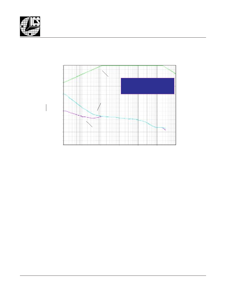
T
YPICAL
P
HASE
N
OISE
AT
148.3516484MH
Z
148.3516484MHz
RMS Phase Noise Jitter
12k to 20MHz = 0.81ps (typical)
0
-10
-20
-30
-40
-50
-60
-70
-80
-90
-100
-110
-120
-130
-140
-150
-160
-170
-180
-190
100
1k
10k
100k
1M
10M
100M
O
FFSET
F
REQUENCY
(H
Z
)
P
HASE
N
OISE
(
dBc
)
H
Z
Phase Noise Result by adding
Fibre Channel Filter to raw data
Raw Phase Noise Data
Fibre Channel Filter

810001BK-21
www.icst.com/products/hiperclocks.html
REV. A AUGUST 12, 2005
10
Integrated
Circuit
Systems, Inc.
ICS810001-21
F
EMTO
C
LOCKS
TM D
UAL
VCXO V
IDEO
PLL
PRELIMINARY
P
ARAMETER
M
EASUREMENT
I
NFORMATION
O
UTPUT
D
UTY
C
YCLE
/P
ULSE
W
IDTH
/tP
ERIOD
P
HASE
J
ITTER
3.3V O
UTPUT
L
OAD
AC T
EST
C
IRCUIT
SCOPE
Qx
LVCMOS
1.65V±5%
O
UTPUT
R
ISE
/F
ALL
T
IME
-1.65V±5%
Clock
Outputs
20%
80%
80%
20%
t
R
t
F
t
PERIOD
t
PW
t
PERIOD
odc =
V
DDO
2
x 100%
t
PW
Q
V
EE
V
DD
,
V
DDA
, V
DDO,
V
DDX
Phase Noise Mask
Offset Frequency
f
1
f
2
Phase Noise Plot
RMS Jitter = Area Under the Masked Phase Noise Plot
Noise P
o
w
er
810001BK-21
www.icst.com/products/hiperclocks.html
REV. A AUGUST 12, 2005
11
Integrated
Circuit
Systems, Inc.
ICS810001-21
F
EMTO
C
LOCKS
TM D
UAL
VCXO V
IDEO
PLL
PRELIMINARY
A
PPLICATION
I
NFORMATION
r
e
d
i
v
i
D
L
L
P
O
X
C
V
n
o
i
t
c
e
l
e
S
n
o
i
t
c
e
l
e
S
t
n
e
n
o
p
m
o
C
r
e
t
l
i
F
p
o
o
L
e
c
n
a
m
r
o
f
r
e
P
L
L
P
O
X
C
V
r
e
t
l
i
F
p
o
o
L
e
l
p
m
a
x
E
r
e
b
m
u
N
)
e
u
l
a
V
M
(
r
e
d
i
v
i
D
B
F
t
e
s
R
k
(
)
t
e
s
I
)
A
µ
(
s
R
k
(
)
s
C
)
F
µ
(
p
C
)
F
p
(
L
L
P
O
X
C
V
)
B
d
3
-
/
z
H
(
W
B
p
o
o
L
r
o
t
c
a
F
g
n
i
p
m
a
D
1
0
0
1
,
0
0
0
1
2
.
2
0
0
5
1
6
2
3
3
0
.
0
0
0
5
1
0
0
2
4
.
1
1
4
.
4
0
5
2
1
6
2
8
6
0
.
0
0
0
3
3
0
0
1
4
.
1
2
4
.
4
0
5
2
6
.
3
5
5
.
1
0
0
0
8
6
0
2
4
.
1
3
1
0
0
4
,
0
0
0
4
2
.
2
0
0
5
9
9
4
3
3
0
.
0
0
0
5
1
0
0
1
3
.
1
4
2
.
2
0
0
5
1
6
2
5
1
.
0
0
0
8
6
0
5
5
.
1
5
2
.
2
0
0
5
5
0
1
1
0
0
0
3
3
0
2
6
.
1
6
2
9
,
1
9
4
.
4
0
5
2
2
.
3
2
1
0
0
0
3
3
0
0
1
6
.
1
7
0
0
6
4
.
4
0
5
2
1
6
2
8
6
0
.
0
0
0
2
2
0
7
1
8
.
1
8
0
0
8
5
2
1
6
.
1
0
6
9
5
0
1
5
.
1
0
0
0
1
,
0
0
0
1
0
0
1
4
.
1
8
2
7
1
,
6
2
7
1
8
5
1
4
0
0
4
,
0
0
0
4
7
2
7
.
0
8
2
7
1
,
6
2
7
1
2
.
2
0
0
5
0
0
0
1
1
0
.
0
0
7
4
0
0
1
5
.
1
9
E
XAMPLE
L
OOP
F
ILTER
C
OMPONENT
V
ALUES
FOR
V
ARIOUS
VCXO D
IVIDER
S
ELECTIONS
810001BK-21
www.icst.com/products/hiperclocks.html
REV. A AUGUST 12, 2005
12
Integrated
Circuit
Systems, Inc.
ICS810001-21
F
EMTO
C
LOCKS
TM D
UAL
VCXO V
IDEO
PLL
PRELIMINARY
A
PPLICATION
E
XAMPLE
1: 27MH
Z
TO
74.25MH
Z
Charge
Pump
VCXO
V3:V0 = 0000
Phase
Detector
Q = 74.25 MHz
Output
Divider
00 = 4
01 = 8
10 = 12
11 = 18
VCXO Feedback Divider
= 1000
VCXO Input
Pre-Divider
= 1000
VCXO Jitter Attenuation PLL
XT
AL_IN0
XT
AL_
OUT0
XT
AL_IN
1
XT
AL_
OUT1
LF1
LF0
ISET
VCXO
Divider
Table
OE = 1
XT
AL_SEL = 1
0
1
MF = 0
MR = 0
Master Reset
0
1
CLK0 = 27 MHz
CLK1 = GND
CLK_SEL = 0
N1:N0 = 01
4
2
11
10
10
11
01
01
10
11
00
2
nBP1:nBP0 = 11
FemtoClock
Frequency Multiplier
= x 22
26.973 MHz
27.000 MHz
RSET = 4.4k
(Makes ISET = 250
A)
Cp = 3300 pf
Cs = 0.068
F
Rs = 261 k
VCXO PLL Loop Characteristics with this configuration:
- Bandwidth (-3dB) = 100 Hz
- Damping Factor = 1.4
810001BK-21
www.icst.com/products/hiperclocks.html
REV. A AUGUST 12, 2005
13
Integrated
Circuit
Systems, Inc.
ICS810001-21
F
EMTO
C
LOCKS
TM D
UAL
VCXO V
IDEO
PLL
PRELIMINARY
A
PPLICATION
E
XAMPLE
2: 27MH
Z
TO
74.175MH
Z
Charge
Pump
VCXO
V3:V0 = 0001
Phase
Detector
Q = 74.125 MHz
Output
Divider
00 = 4
01 = 8
10 = 12
11 = 18
VCXO Feedback Divider
= 1000
VCXO Input
Pre-Divider
= 1001
VCXO Jitter Attenuation PLL
XT
AL_IN
0
XT
AL_
OUT0
XT
AL_IN
1
XT
AL_
OUT1
LF1
LF0
ISET
VCXO
Divider
Table
OE = 1
XT
AL_SEL = 0
0
1
MF = 0
MR = 0
Master Reset
0
1
CLK0 = 27 MHz
CLK1 = GND
CLK_SEL = 0
N1:N0 = 01
4
2
11
10
10
11
01
01
10
11
00
2
nBP1:nBP0 = 11
FemtoClock
Frequency Multiplier
= x 22
26.973 MHz
27.000 MHz
VCXO PLL Loop Characteristics with this configuration:
- Bandwidth (-3dB) = 100 Hz
- Damping Factor = 1.4
RSET = 4.4k
(Makes ISET = 250
A)
Cp = 3300 pf
Cs = 0.068
F
Rs = 261 k

810001BK-21
www.icst.com/products/hiperclocks.html
REV. A AUGUST 12, 2005
14
Integrated
Circuit
Systems, Inc.
ICS810001-21
F
EMTO
C
LOCKS
TM D
UAL
VCXO V
IDEO
PLL
PRELIMINARY
D
ESCRIPTION
OF
THE
PLL S
TAGES
The ICS843002-21 is a two stage device, a VCXO PLL fol-
lowed by a low phase noise FemtoClock frequency multiplier.
The VCXO uses an external pullable crystal which can be
pulled ±100ppm by the VCXO PLL circuitry to phase lock it to
the input reference frequency. There are two VCXO crystal
ports in order to provide VCXO frequency versatility. For HDTV
applications, this allows the use of a 26.973027MHz crystal
for the generation of 74.175MHz, or a 27.00MHz crystal for
the generation of 74.25MHz, for example.
The VCXO output frequency can be output directly from the
device, or it can be passed to the FemtoClock frequency
multiplier which will multiply it up to a higher frequency.
VCXO PLL L
OOP
R
ESPONSE
C
ONSIDERATIONS
Loop response characteristics of the VCXO PLL is affected
by the VCXO feedback divider value (bandwidth and damping
factor), and by the external loop filter components (bandwidth,
damping factor, and 2
nd
frequency response). A practical range
of VCXO PLL bandwidth is from about 1Hz to about 1kHz.
The setting of VCXO PLL bandwidth and damping factor is
covered later in this document. A PC based PLL bandwidth
calculator is also under development. For assistance with loop
bandwidth suggestions or value calculation, please contact
ICS applications.
Table 3A shows frequency translation configuration examples.
Note that in the first two V3:V0 selections the VCXO PLL feed-
back divider is the same value of 1000. This means the VCXO
PLL loop response (bandwidth and damping factor) will be the
same for all of these settings.
The same is true for V3:V0 = 0010 through 0110. This means
the device can be configured to translate between 74.175MHz,
74.25MHz, and 27MHz (from any one to another, all nine com-
binations) and it will maintain the same loop response char-
acteristics. This is also true for V3:V0 = 1000 through 1010.
For high VCXO PLL feedback divider values, the phase de-
tector rate, and therefore loop filter charge pulse rate, is greatly
reduced. To prevent output clock wander, low leakage capaci-
tors should be used. In addition, when loop bandwidth is low
(say below 20Hz), capacitors with low microphonic sensitiv-
ity should be used. PPS film type capacitors are one type that
perform well in this environment. Below 5Hz, shielding should
be considered to prevent excessive phase wander (low fre-
quency phase jitter or clock phase deviation).
S
ETTING
THE
VCXO PLL L
OOP
R
ESPONSE
The VCXO PLL loop response is determined both by fixed device
characteristics and by other characterizes set by the user. This
includes the values of R
S
, C
S
, C
P
and R
SET
as shown in the
External VCXO PLL Components figure on this page.
The VCXO PLL loop bandwidth is approximated by:
W
HERE
:
R
S
= Value of resistor R
S
in loop filter in Ohms
I
CP
= Charge pump current in amps (see table on page 12)
K
O
= VCXO Gain in Hz/V
Feedback Divider = 1 to 11011 (as determined by inputs
V3:V0)
The above equation calculates the "normalized" loop bandwidth
(denoted as "NBW") which is approximately equal to the - 3dB
bandwidth. NBW does not take into account the effects of
damping factor or the second pole imposed by C
P
. It does,
however, provide a useful approximation of filter performance.
To prevent jitter on the clock output due to modulation of the
VCXO PLL by the phase detector frequency, the following general
rule should be observed:
(Phase Detector) = Input Frequency ˜ Pre-Divider)
The PLL loop damping factor is determined by:
W
HERE
:
C
S
= Value of capacitor C
S
in loop filter in Farads
NBW (VCXO PLL) =
R
S
x I
CP
x K
O
2
x Feedback Divider
NBW (VCXO PLL)
(Phase Detector)
20
DF = x
R
S
2
I
CP
x C
S
x K
O
Feedback Divider
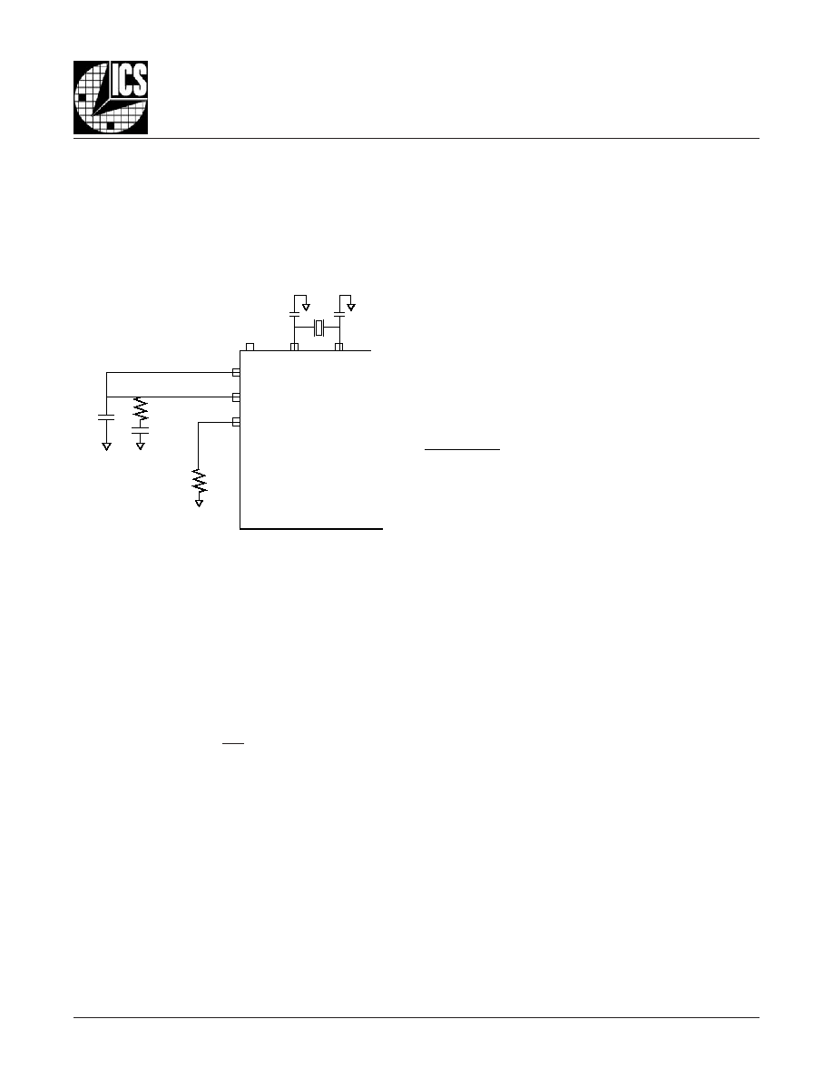
810001BK-21
www.icst.com/products/hiperclocks.html
REV. A AUGUST 12, 2005
15
Integrated
Circuit
Systems, Inc.
ICS810001-21
F
EMTO
C
LOCKS
TM D
UAL
VCXO V
IDEO
PLL
PRELIMINARY
N
OTES
ON
S
ETTING
THE
V
ALUE
OF
C
P
As another general rule, the following relationship should be
maintained between components C
S
and C
P
in the loop filter:
C
P
establishes a second pole in the VCXO PLL loop filter. For
higher damping factors (> 1), calculate the value of C
P
based on
a C
S
value that would be used for a damping factor of 1. This will
minimize baseband peaking and loop instability that can lead to
output jitter.
C
P
also dampens VCXO PLL input voltage modulation by the
charge pump correction pulses. A C
P
value that is too low will
result in increased output phase noise at the phase detector
frequency due to this. In extreme cases where input jitter is high,
charge pump current is high, and C
P
is too small, the VCXO PLL
input voltage can hit the supply or ground rail resulting in non-
linear loop response.
The best way to set the value of C
P
is to use the filter response
software available from ICS (please refer to the following section).
C
P
should be increased in value until it just starts affecting the
passband peak.
N
OTES
ON
E
XTERNAL
C
RYSTAL
L
OAD
C
APACITORS
In the loop filter schematic diagram, capacitors are shown be-
tween pins 27/30 to ground and between pins 38/31 to ground.
These are optional crystal load capacitors which can be used to
center tune the external pullable crystal (the crystal frequency
can only be lowered by adding capacitance, it cannot be raised).
Note that the addition of external load capacitors will decrease
the crystal pull range and the Kvco value.
L
OOP
F
ILTER
R
ESPONSE
S
OFTWARE
Online tools to calculate loop filter response can be found at
www.icst.com. Contact your local sales representative if a tool
cannot be found for this product.
C
P
=
C
S
20
E
XTERNAL
VCXO PLL C
OMPONENTS
In general, the loop damping factor should be 0.7 or greater to
ensure output stability. A higher damping factor will create less
peaking in the passband. A higher damping factor may also
increase lock time and output clock jitter when there is excess
digital noise in the system application, due to the reduced ability
of the PLL to respond to and therefore compensate for phase
noise ingress.
1
2
3
64 27/30 28/31
LF1
LF0
ISET
C
S
R
S
C
P
R
SET
The external crystal devices and loop filter components should
be kept close to the device. Loop filter and crystal PCB
connection traces should be kept short and well separated from
each other and from other signal traces. Other signal traces
shouldnot run underneath the device, the loop filter or crystal
components.

810001BK-21
www.icst.com/products/hiperclocks.html
REV. A AUGUST 12, 2005
16
Integrated
Circuit
Systems, Inc.
ICS810001-21
F
EMTO
C
LOCKS
TM D
UAL
VCXO V
IDEO
PLL
PRELIMINARY
VCXO C
RYSTAL
S
ELECTION
Choosing a crystal with the correct characteristics is one of the
most critical steps in using a Voltage Controlled Crystal Oscillator
(VCXO). The crystal parameters affect the tuning range and
V
C
Control voltage used to tune frequency
C
V
Varactor capacitance, varies due to the change in
control voltage
C
RYSTAL
P
ARAMETER
E
XAMPLES
l
o
b
m
y
S
r
e
t
e
m
a
r
a
P
n
o
i
t
i
d
n
o
C
t
s
e
T
l
a
c
i
p
y
T
t
i
n
U
C
W
O
L
V
e
c
n
a
t
i
c
a
p
a
C
r
o
t
c
a
r
a
V
w
o
L
V
C
V
0
=
4
.
5
1
F
p
C
H
G
I
H
V
e
c
n
a
t
i
c
a
p
a
C
r
o
t
c
a
r
a
V
h
g
i
H
V
C
V
3
.
3
=
6
.
9
2
F
p
V
ARACTOR
P
ARAMETERS
accuracy of a VCXO. Below are the key variables and an
example of using the crystal parameters to calculate the tuning
range of the VCXO.
C
L1,
C
L2
Load tuning capacitance used for fine tuning or
centering nominal frequency
C
S1,
C
S2
Stray Capacitance caused by pads, vias, and other
board parasitics
Oscillator
F
IGURE
1: VCXO O
SCILLATOR
C
IRCUIT
E
XAMPLE
VCXO (Internal)
C
V
C
V
C
L1
C
L2
Optional
C
S1
C
S2
V
C
"Control Voltage"
XTAL
l
o
b
m
y
S
r
e
t
e
m
a
r
a
P
m
u
m
i
n
i
M
l
a
c
i
p
y
T
m
u
m
i
x
a
M
s
t
i
n
U
f
N
y
c
n
e
u
q
e
r
F
l
a
n
i
m
o
N
4
4
.
9
1
z
H
M
f
T
e
c
n
a
r
e
l
o
T
y
c
n
e
u
q
e
r
F
0
2
±
m
p
p
f
S
y
t
il
i
b
a
t
S
y
c
n
e
u
q
e
r
F
0
2
±
m
p
p
e
g
n
a
R
e
r
u
t
a
r
e
p
m
e
T
g
n
i
t
a
r
e
p
O
0
0
7
C
∞
C
L
e
c
n
a
t
i
c
a
p
a
C
d
a
o
L
2
1
F
p
C
O
e
c
n
a
t
i
c
a
p
a
C
t
n
u
h
S
4
F
p
C
0
C
/
1
o
i
t
a
R
y
t
il
i
b
a
ll
u
P
0
2
2
0
4
2
R
S
E
e
c
n
a
t
s
i
s
e
R
s
e
i
r
e
S
t
n
e
l
a
v
i
u
q
E
0
2
l
e
v
e
L
e
v
i
r
D
1
W
m
C
∞
5
2
@
g
n
i
g
A
r
a
e
y
r
e
p
3
±
m
p
p
n
o
i
t
a
r
e
p
O
f
o
e
d
o
M
l
a
t
n
e
m
e
d
n
u
F

810001BK-21
www.icst.com/products/hiperclocks.html
REV. A AUGUST 12, 2005
17
Integrated
Circuit
Systems, Inc.
ICS810001-21
F
EMTO
C
LOCKS
TM D
UAL
VCXO V
IDEO
PLL
PRELIMINARY
The example above will ensure a total pull range of ±113.25
ppm with an APR of ±58.25ppm. Many times, board designers
may select their own crystal based on their application. If the
application requires a tighter APR, a crystal with better pullability
F
ORMULAS
C
LOW
=
(C
L1
+ C
S1
+ C
V_LOW
) ∑ (C
L2
+ C
S2
+ C
V_LOW
)
(C
L1
+ C
S1
+ C
V_LOW
) + (C
L2
+ C
S2
+ C
V_LOW
)
C
HIGH
=
(C
L1
+ C
S1
+ C
V_HIGH
∑ (C
L2
+ C
S2
+ C
V_HIGH
)
(C
L1
+ C
S1
+ C
V_HIGH
) + (C
L2
+ C
S2
+ C
V_HIGH
)
C
Low
is the effective capacitance due to the low varactor
capacitance, load capacitance and stray capacitance.
C
Low
determines the high frequency component on the
TPR (Total Pull Range).
C
High
is the effective capacitance due to the high varactor
capacitance, load capacitance and stray capacitance.
C
High
determines the low frequency component on the
TPR (Total Pull Range).
E
XAMPLE
C
ALCULATIONS
Using the tables and figures above, we can now calculate the
TPR and APR of the VCXO using the example crystal
parameters. For the numerical example below there were some
assumptions made. First, the stray capacitance (C
S1
, C
S2
), which
is all the excess capacitance due to board parasitic, is 4pF.
Second, the expected lifetime of the project is 5 years; hence
the inaccuracy due to aging is ±15ppm. Third, though many
boards will not require load tuning capacitors (C
L1
, C
L2
), it is
recommended for long-term consistent performance of the
system that two tuning capacitor pads be placed into every
design. Typical values for the load tuning capacitors will range
from 0 to 4pF.
AbsolutePullRange (APR) = TotalPullRange ≠ (FrequencyTolerance + FrequencyStability + Aging)
TPR =
1
2 ∑ C
0
/C
1
∑ (1+C
LOW
/C
0
)
1
2 ∑ C
0
/C
1
∑ (1+C
HIGH
/C
0
)
≠
∑ 10
6
(
)
C
LOW
=
(0 + 4pF + 15.4pF) ∑ (0 + 4pF + 15.4pF)
(0 + 4pF + 15.4pF) + (0 + 4pF + 15.4pF)
= 9.7pF
C
HIGH
=
(0 + 4pF + 29.6pF) ∑ (0 + 4pF + 29.6pF)
(0 + 4pF + 29.6pF) + (0 + 4pF + 29.6pF)
= 16.8pF
TPR = ±113.25ppm
APR = 113.25ppm ≠ (20ppm + 20ppm + 15ppm) = ±58.25ppm
TPR =
1
2 ∑ 220 ∑ (1+9.7pF/4pF)
1
2 ∑ 220 ∑ (1+16.8pF/4pF)
≠
∑ 10
6
= 226.5ppm
(
)
(C0/C1 ratio) can be used. Also, with the equations above, one
can vary the frequency tolerance, temperature stability, and
aging or shunt capacitance to achieve the required pullability.
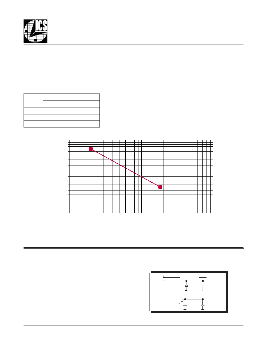
810001BK-21
www.icst.com/products/hiperclocks.html
REV. A AUGUST 12, 2005
18
Integrated
Circuit
Systems, Inc.
ICS810001-21
F
EMTO
C
LOCKS
TM D
UAL
VCXO V
IDEO
PLL
PRELIMINARY
As in any high speed analog circuitry, the power supply pins
are vulnerable to random noise. The ICS810001-21 provides
separate power supplies to isolate any high switching
noise from the outputs to the internal PLL. V
DD
, V
DDA
, V
DDx
, and
V
DDO
should be individually connected to the power supply
plane through vias, and bypass capacitors should be
used for each pin. To achieve optimum jitter performance,
power supply isolation is required.
Figure 3
illustrates how
a 10
resistor along with a 10F and a .01F bypass
capacitor should be connected to each V
DDA
pin.
P
OWER
S
UPPLY
F
ILTERING
T
ECHNIQUES
F
IGURE
3. P
OWER
S
UPPLY
F
ILTERING
10
V
DDA
10
F
.01
F
3.3V
.01
F
V
DD
N
OTES
ON
S
ETTING
C
HARGE
P
UMP
C
URRENT
The recommended range for the charge pump current is 50
A
to 300
A. Below 50A, loop filter charge leakage, due to PCB or
capacitor leakage, can become a problem. This loop filter leakage
can cause locking problems, output clock cycle slips, or low
frequency phase noise.
1E-3
100E-6
10E-6
1k
10k
100k
R
SET
,
I
CP
, Amps
R
T
E
S
I
(
t
n
e
r
r
u
C
p
m
u
P
e
g
r
a
h
C
P
C
)
k
6
.
7
1
A
µ
5
.
2
6
k
8
.
8
A
µ
5
2
1
k
4
.
4
A
µ
0
5
2
k
2
.
2
A
µ
0
0
5
F
IGURE
2. C
HARGE
P
UMP
C
URRENT
VS
. V
ALUE
OF
R
SET
(
EXTERNAL
RESISTOR
) G
RAPH
As can be seen in the loop bandwidth and damping factor
equations or by using the filter response software available from
ICS, increasing charge pump current (I
CP
) increases both
bandwidth and damping factor.
C
HARGE
P
UMP
C
URRENT
, E
XAMPLE
S
ETTINGS

810001BK-21
www.icst.com/products/hiperclocks.html
REV. A AUGUST 12, 2005
19
Integrated
Circuit
Systems, Inc.
ICS810001-21
F
EMTO
C
LOCKS
TM D
UAL
VCXO V
IDEO
PLL
PRELIMINARY
R
ELIABILITY
I
NFORMATION
T
RANSISTOR
C
OUNT
The transistor count for ICS810001-21 is: 9365
T
ABLE
7.
JA
VS
. A
IR
F
LOW
T
ABLE
FOR
32 L
EAD
VFQFN
JA
vs. 0 Air Flow (Linear Feet per Minute)
0
Multi-Layer PCB, JEDEC Standard Test Boards
34.8∞C/W

810001BK-21
www.icst.com/products/hiperclocks.html
REV. A AUGUST 12, 2005
20
Integrated
Circuit
Systems, Inc.
ICS810001-21
F
EMTO
C
LOCKS
TM D
UAL
VCXO V
IDEO
PLL
PRELIMINARY
T
ABLE
8. P
ACKAGE
D
IMENSIONS
P
ACKAGE
O
UTLINE
AND
D
IMENSIONS
- K S
UFFIX
FOR
32 L
EAD
VFQFN
Reference Document: JEDEC Publication 95, MO-220
N
O
I
T
A
I
R
A
V
C
E
D
E
J
S
R
E
T
E
M
I
L
L
I
M
N
I
S
N
O
I
S
N
E
M
I
D
L
L
A
L
O
B
M
Y
S
2
-
D
H
H
V
M
U
M
I
N
I
M
L
A
N
I
M
O
N
M
U
M
I
X
A
M
N
2
3
A
0
8
.
0
-
-
0
0
.
1
1
A
0
-
-
5
0
.
0
3
A
.
f
e
R
5
2
.
0
b
8
1
.
0
5
2
.
0
0
3
.
0
N
D
8
N
E
8
D
C
I
S
A
B
0
0
.
5
2
D
5
2
.
1
5
2
.
2
5
2
.
3
E
C
I
S
A
B
0
0
.
5
2
E
5
2
.
1
5
2
.
2
5
2
.
3
e
C
I
S
A
B
0
5
.
0
L
0
3
.
0
0
4
.
0
0
5
.
0

810001BK-21
www.icst.com/products/hiperclocks.html
REV. A AUGUST 12, 2005
21
Integrated
Circuit
Systems, Inc.
ICS810001-21
F
EMTO
C
LOCKS
TM D
UAL
VCXO V
IDEO
PLL
PRELIMINARY
T
ABLE
9. O
RDERING
I
NFORMATION
While the information presented herein has been checked for both accuracy and reliability, Integrated Circuit Systems, Incorporated (ICS) assumes no responsibility for either its use
or for infringement of any patents or other rights of third parties, which would result from its use. No other circuits, patents, or licenses are implied. This product is intended for use
in normal commercial applications. Any other applications such as those requiring extended temperature range, high reliability, or other extraordinary environmental requirements are
not recommended without additional processing by ICS. ICS reserves the right to change any circuitry or specifications without notice. ICS does not authorize or warrant any ICS
product for use in life support devices or critical medical instruments.
The aforementioned trademarks, HiPerClockSTM and F
EMTO
C
LOCKS
TM are a trademark of Integrated Circuit Systems, Inc. or its subsidiaries in the United States and/or other countries.
r
e
b
m
u
N
r
e
d
r
O
/
t
r
a
P
g
n
i
k
r
a
M
e
g
a
k
c
a
P
g
n
i
g
a
k
c
a
P
g
n
i
p
p
i
h
S
e
r
u
t
a
r
e
p
m
e
T
1
2
-
K
B
1
0
0
0
1
8
S
C
I
1
2
B
1
0
0
0
1
S
C
I
N
F
Q
F
V
d
a
e
L
2
3
y
a
r
t
C
∞
0
7
o
t
C
∞
0
T
1
2
-
K
B
1
0
0
0
1
8
S
C
I
1
2
B
1
0
0
0
1
S
C
I
N
F
Q
F
V
d
a
e
L
2
3
l
e
e
r
&
e
p
a
t
0
0
5
2
C
∞
0
7
o
t
C
∞
0