 | –≠–ª–µ–∫—Ç—Ä–æ–Ω–Ω—ã–π –∫–æ–º–ø–æ–Ω–µ–Ω—Ç: ICS810-06 | –°–∫–∞—á–∞—Ç—å:  PDF PDF  ZIP ZIP |
Document Outline
- General Description
- Features
- Block Diagram
- Pin Assignment
- Pin Descriptions
- Pin Characteristics
- Absolute Maximum Ratings
- 3.3V Power Supply DC Characteristics
- 3.3V/2.5V Power Supply DC Characteristics
- LVCMOS DC Characteristics
- 3.3V AC Characteristics
- 3.3V/2.5V AC Characteristics
- 3.3V/1.8V AC Characteristics
- 2.5V AC Characteristics
- 2.5V/1.8V AC Characteristics
- Typical Phase Noise Plot
- Parameter Measurement Information
- Parameter Measurement Information, continued
- Application Information
- VCXO Crystal Slection
- VCXO Oscillator Circuit Diagram
- Example Crystal Parameters Table
- Varactor Parameters Table
- Formulas
- Example Calculations
- Recommendations for Unused Input and Output Pins
- Schematic Example
- Reliability Information
- Transistor Count
- Package Outline
- Package Dimensions
- Ordering Information

81006AK
www.icst.com/products/hiperclocks.html
REV. A JANUARY 4, 2006
1
Integrated
Circuit
Systems, Inc.
ICS81006
VCXO-
TO
-6 LVCMOS O
UTPUTS
VCXO
0: ˜1
1: ˜2
SYNC
SYNC
LP Filter
G
ENERAL
D
ESCRIPTION
The ICS81006 is a high performance, low
j i t t e r / l o w p h a s e n o i s e V C X O a n d i s a
member of the HiPerClockSTM family of high
performance clock solutions from ICS. The
I C S 8 1 0 0 6 w o r k s i n c o n j u n c t i o n w i t h a
pullable crystal to generate an output clock over the
range of 12MHz - 40MHz and has 6 LVCMOS outputs,
effectively integrating a fanout buffer function.
The frequency of the VCXO is adjusted by the VC control
voltage input. The output range is ±100ppm around the
nominal crystal frequency. The VC control voltage range
is 0 - V
DD
. The device is packaged in a small 4mm x 4mm
V F Q F N p a c k a g e a n d i s i d e a l f o r u s e o n s p a c e
constrained boards typically encountered in ADSL/
VDSL applications.
F
EATURES
∑ Six LVCMOS/LVTTL outputs, 20 nominal
output impedance
∑ Output Q5 can be selected for ˜1 or ˜2 frequency relative
to the crystal frequency
∑ Output frequency range: 12MHz to 40MHz
∑ Crystal pull range: ± 90ppm (typical)
∑ Synchronous output enable places outputs in High-Z state
∑ On-chip filter on VIN to suppress noise modulation of VCXO
∑ V
DD
/V
DDO
combinations
3.3V/3.3V
3.3V/2.5V
3.3V/1.8V
2.5V/2.5V
2.5V/1.8V
∑ 4mm x 4mm 20 Lead VFQFN package is ideal for space
constrained designs
∑ 0∞C to 70∞C ambient operating temperature
∑ Available in both standard and lead-free RoHS compliant
packages
HiPerClockSTM
ICS
B
LOCK
D
IAGRAM
P
IN
A
SSIGNMENT
OE0
VC
XTAL_IN
XTAL_OUT
DIV_SEL_Q5
OE1
Q0
Q1
Q2
Q3
Q4
Q5
(Pullup)
(Pulldown)
XTAL_IN
XTAL_OUT
V
DD
VC
DIV_SEL_Q5
GND
Q2
V
DDO
Q3
GND
OE1
GND
Q5
V
DDO
Q4
OE0
GND
Q0
V
DDO
Q1
1
2
3
4
5
20 19 18 17 16
ICS81006
20-Lead VFQFN
4mm x 4mm x 0.95 package body
K Package
Top View
6 7 8 9 10
15
14
13
12
11
(Pullup)
81006AK
www.icst.com/products/hiperclocks.html
REV. A JANUARY 4, 2006
2
Integrated
Circuit
Systems, Inc.
ICS81006
VCXO-
TO
-6 LVCMOS O
UTPUTS
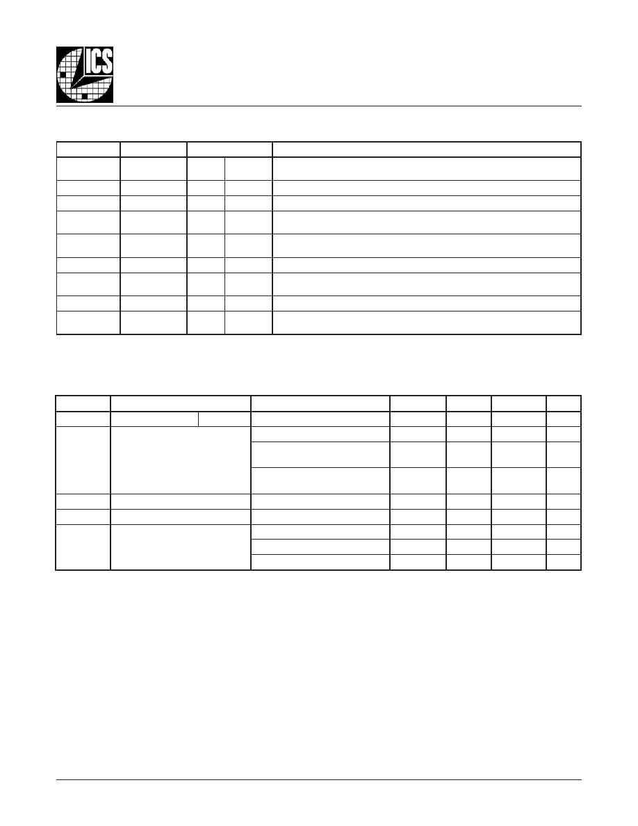
T
ABLE
2. P
IN
C
HARACTERISTICS
T
ABLE
1. P
IN
D
ESCRIPTIONS
r
e
b
m
u
N
e
m
a
N
e
p
y
T
n
o
i
t
p
i
r
c
s
e
D
2
,
1
,
N
I
_
L
A
T
X
T
U
O
_
L
A
T
X
t
u
p
n
I
.
t
u
p
n
i
e
h
t
s
i
N
I
_
L
A
T
X
.
e
c
a
f
r
e
t
n
i
r
o
t
a
ll
i
c
s
o
l
a
t
s
y
r
C
.
t
u
p
t
u
o
e
h
t
s
i
T
U
O
_
L
A
T
X
3
V
D
D
r
e
w
o
P
.
n
i
p
y
l
p
p
u
s
e
r
o
C
4
C
V
t
u
p
n
I
.
t
u
p
n
i
e
g
a
t
l
o
v
l
o
r
t
n
o
C
5
5
Q
_
L
E
S
_
V
I
D
t
u
p
n
I
n
w
o
d
ll
u
P
,
H
G
I
H
n
e
h
W
.
1
˜
,
W
O
L
n
e
h
W
.
t
u
p
t
u
o
5
Q
r
o
f
n
i
p
t
c
e
l
e
s
r
e
d
i
v
i
d
t
u
p
t
u
O
.
s
l
e
v
e
l
e
c
a
f
r
e
t
n
i
L
T
T
V
L
/
S
O
M
C
V
L
,
2
˜
6
1
E
O
t
u
p
n
I
p
u
ll
u
P
.
d
e
l
b
a
n
e
s
i
t
u
p
t
u
o
5
Q
,
H
G
I
H
n
e
h
W
.
n
i
p
e
l
b
a
n
e
t
u
p
t
u
O
.
s
l
e
v
e
l
e
c
a
f
r
e
t
n
i
L
T
T
V
L
/
S
O
M
C
V
L
.
e
t
a
t
s
Z
i
H
o
t
5
Q
s
e
c
r
o
f
,
W
O
L
n
e
h
W
9
1
,
5
1
,
1
1
,
7
D
N
G
r
e
w
o
P
.
d
n
u
o
r
g
y
l
p
p
u
s
r
e
w
o
P
,
2
1
,
0
1
,
8
8
1
,
6
1
,
4
1
,
3
Q
,
4
Q
,
5
Q
0
Q
,
1
Q
,
2
Q
t
u
p
t
u
O
.
s
l
e
v
e
l
e
c
a
f
r
e
t
n
i
L
T
T
V
L
/
S
O
M
C
V
L
.
s
t
u
p
t
u
o
k
c
o
l
c
d
e
d
n
e
-
e
l
g
n
i
S
5
1
.
e
c
n
a
d
e
p
m
i
t
u
p
t
u
o
l
a
c
i
p
y
t
7
1
,
3
1
,
9
V
O
D
D
r
e
w
o
P
.
s
n
i
p
y
l
p
p
u
s
t
u
p
t
u
O
0
2
0
E
O
t
u
p
n
I
p
u
ll
u
P
n
e
h
W
.
d
e
l
b
a
n
e
e
r
a
s
t
u
p
t
u
o
4
Q
:
0
Q
,
H
G
I
H
n
e
h
W
.
n
i
p
e
l
b
a
n
e
t
u
p
t
u
O
.
s
l
e
v
e
l
e
c
a
f
r
e
t
n
i
L
T
T
V
L
/
S
O
M
C
V
L
.
e
t
a
t
s
Z
i
H
o
t
4
Q
:
0
Q
s
e
c
r
o
f
,
W
O
L
:
E
T
O
N
p
u
ll
u
P
d
n
a
n
w
o
d
ll
u
P
.
s
e
u
l
a
v
l
a
c
i
p
y
t
r
o
f
,
s
c
i
t
s
i
r
e
t
c
a
r
a
h
C
n
i
P
,
2
e
l
b
a
T
e
e
S
.
s
r
o
t
s
i
s
e
r
t
u
p
n
i
l
a
n
r
e
t
n
i
o
t
s
r
e
f
e
r
l
o
b
m
y
S
r
e
t
e
m
a
r
a
P
s
n
o
i
t
i
d
n
o
C
t
s
e
T
m
u
m
i
n
i
M
l
a
c
i
p
y
T
m
u
m
i
x
a
M
s
t
i
n
U
C
N
I
e
c
n
a
t
i
c
a
p
a
C
t
u
p
n
I
1
E
O
,
0
E
O
4
F
p
C
D
P
e
c
n
a
t
i
c
a
p
a
C
n
o
i
t
a
p
i
s
s
i
D
r
e
w
o
P
V
D
D
V
=
O
D
D
V
5
6
4
.
3
=
3
F
p
V
D
D
,
V
5
2
6
.
2
r
o
V
5
6
4
.
3
=
V
O
D
D
V
5
2
6
.
2
=
4
F
p
V
D
D
,
V
5
2
6
.
2
r
o
V
5
6
4
.
3
=
V
O
D
D
V
2
=
6
F
p
R
P
U
L
L
U
P
r
o
t
s
i
s
e
R
p
u
ll
u
P
t
u
p
n
I
1
5
k
R
N
W
O
D
L
L
U
P
r
o
t
s
i
s
e
R
n
w
o
d
ll
u
P
t
u
p
n
I
1
5
k
R
T
U
O
e
c
n
a
d
e
p
m
I
t
u
p
t
u
O
V
O
D
D
V
3
.
3
=
0
2
V
O
D
D
V
5
.
2
=
5
2
V
O
D
D
V
8
.
1
=
8
3
81006AK
www.icst.com/products/hiperclocks.html
REV. A JANUARY 4, 2006
3
Integrated
Circuit
Systems, Inc.
ICS81006
VCXO-
TO
-6 LVCMOS O
UTPUTS
A
BSOLUTE
M
AXIMUM
R
ATINGS
Supply Voltage, V
DD
4.6V
Inputs, V
I
-0.5V to V
DD
+ 0.5 V
Outputs, V
O
-0.5V to V
DD
+ 0.5V
Package Thermal Impedance,
JA
38.5∞C/W (0 mps)
Storage Temperature, T
STG
-65∞C to 150∞C
NOTE: Stresses beyond those listed under Absolute
Maximum Ratings may cause permanent damage to the
device. These ratings are stress specifications only. Functional
operation of product at these conditions or any conditions be-
yond those listed in the
DC Characteristics
or
AC Character-
istics
is not implied. Exposure to absolute maximum rating
conditions for extended periods may affect product reliability.
T
ABLE
3A. P
OWER
S
UPPLY
DC C
HARACTERISTICS
,
V
DD
= 3.3V±5%, V
DDO
= 3.3V±5% = 2.5V±5%
= 1.8V±0.2V, T
A
= 0∞C
TO
70∞C
T
ABLE
3B. P
OWER
S
UPPLY
DC C
HARACTERISTICS
,
V
DD
= 2.5V±5%, V
DDO
= 2.5V±5%
= 1.8V±0.2V, T
A
= 0∞C
TO
70∞C
l
o
b
m
y
S
r
e
t
e
m
a
r
a
P
s
n
o
i
t
i
d
n
o
C
t
s
e
T
m
u
m
i
n
i
M
l
a
c
i
p
y
T
m
u
m
i
x
a
M
s
t
i
n
U
V
D
D
e
g
a
t
l
o
V
y
l
p
p
u
S
e
r
o
C
5
3
1
.
3
3
.
3
5
6
4
.
3
V
V
O
D
D
e
g
a
t
l
o
V
y
l
p
p
u
S
t
u
p
t
u
O
5
3
1
.
3
3
.
3
5
6
4
.
3
V
5
7
3
.
2
5
.
2
5
2
6
.
2
V
6
.
1
8
.
1
0
.
2
V
I
D
D
t
n
e
r
r
u
C
y
l
p
p
u
S
r
e
w
o
P
0
5
A
m
I
O
D
D
t
n
e
r
r
u
C
y
l
p
p
u
S
t
u
p
t
u
O
0
2
A
m
l
o
b
m
y
S
r
e
t
e
m
a
r
a
P
s
n
o
i
t
i
d
n
o
C
t
s
e
T
m
u
m
i
n
i
M
l
a
c
i
p
y
T
m
u
m
i
x
a
M
s
t
i
n
U
V
D
D
e
g
a
t
l
o
V
y
l
p
p
u
S
e
r
o
C
5
7
3
.
2
5
.
2
5
2
6
.
2
V
V
O
D
D
e
g
a
t
l
o
V
y
l
p
p
u
S
t
u
p
t
u
O
5
7
3
.
2
5
.
2
5
2
6
.
2
V
6
.
1
8
.
1
0
.
2
V
I
D
D
t
n
e
r
r
u
C
y
l
p
p
u
S
r
e
w
o
P
0
5
A
m
I
O
D
D
t
n
e
r
r
u
C
y
l
p
p
u
S
t
u
p
t
u
O
0
2
A
m
T
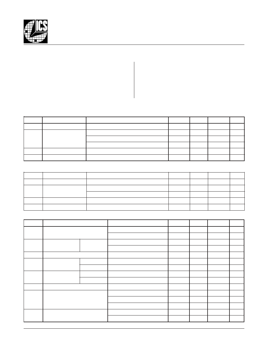
ABLE
3C. LVCMOS/LVTTL DC C
HARACTERISTICS
,
T
A
= 0∞C
TO
85∞C
l
o
b
m
y
S
r
e
t
e
m
a
r
a
P
s
n
o
i
t
i
d
n
o
C
t
s
e
T
m
u
m
i
n
i
M
l
a
c
i
p
y
T
m
u
m
i
x
a
M
s
t
i
n
U
V
H
I
e
g
a
t
l
o
V
h
g
i
H
t
u
p
n
I
V
D
D
%
5
±
V
3
.
3
=
2
V
D
D
3
.
0
+
V
V
D
D
%
5
±
V
5
.
2
=
7
.
1
V
D
D
3
.
0
+
V
V
L
I
e
g
a
t
l
o
V
w
o
L
t
u
p
n
I
,
1
E
O
,
0
E
O
5
Q
_
L
E
S
_
V
I
D
V
D
D
%
5
±
V
3
.
3
=
3
.
0
-
8
.
0
V
V
D
D
%
5
±
V
5
.
2
=
3
.
0
-
7
.
0
V
C
V
e
g
a
t
l
o
V
l
o
r
t
n
o
C
O
X
C
V
0
V
D
D
V
I
H
I
t
n
e
r
r
u
C
h
g
i
H
t
u
p
n
I
5
Q
_
L
E
S
_
V
I
D
V
D
D
%
5
±
V
5
.
2
r
o
V
3
.
3
=
0
5
1
A
µ
1
E
O
,
0
E
O
V
D
D
%
5
±
V
5
.
2
r
o
V
3
.
3
=
5
A
µ
I
L
I
t
n
e
r
r
u
C
w
o
L
t
u
p
n
I
5
Q
_
L
E
S
_
V
I
D
V
D
D
%
5
±
V
5
.
2
r
o
V
3
.
3
=
5
-
A
µ
1
E
O
,
0
E
O
V
D
D
%
5
±
V
5
.
2
r
o
V
3
.
3
=
0
5
1
-
A
µ
I
I
n
i
p
C
V
f
o
t
n
e
r
r
u
C
t
u
p
n
I
V
D
D
V
5
2
6
.
2
r
o
V
5
6
4
.
3
=
0
0
1
-
0
0
1
A
µ
V
H
O
;
e
g
a
t
l
o
V
h
g
i
H
t
u
p
t
u
O
1
E
T
O
N
V
O
D
D
%
5
±
V
3
.
3
=
6
.
2
V
V
O
D
D
%
5
±
V
5
.
2
=
8
.
1
V
V
O
D
D
V
2
.
0
±
V
8
.
1
=
5
.
1
V
V
L
O
;
e
g
a
t
l
o
V
w
o
L
t
u
p
t
u
O
1
E
T
O
N
V
O
D
D
%
5
±
V
5
.
2
r
o
V
3
.
3
=
5
.
0
V
V
O
D
D
V
2
.
0
±
V
8
.
1
=
4
.
0
V
0
5
h
t
i
w
d
e
t
a
n
i
m
r
e
t
s
t
u
p
t
u
O
:
1
E
T
O
N
V
o
t
O
D
D
.
s
m
a
r
g
a
i
d
"
t
i
u
c
r
i
C
t
s
e
T
d
a
o
L
"
,
n
o
i
t
c
e
s
t
n
e
m
e
r
u
s
a
e
M
r
e
t
e
m
a
r
a
P
e
e
S
.
2
/
81006AK
www.icst.com/products/hiperclocks.html
REV. A JANUARY 4, 2006
4
Integrated
Circuit
Systems, Inc.
ICS81006
VCXO-
TO
-6 LVCMOS O
UTPUTS
T
ABLE
4A. AC C
HARACTERISTICS
,
V
DD
= V
DDO
= 3.3V±5%, T
A
= 0∞C
TO
70∞C
l
o
b
m
y
S
r
e
t
e
m
a
r
a
P
s
n
o
i
t
i
d
n
o
C
t
s
e
T
m
u
m
i
n
i
M
l
a
c
i
p
y
T
m
u
m
i
x
a
M
s
t
i
n
U
f
T
U
O
y
c
n
e
u
q
e
r
F
t
u
p
t
u
O
2
1
4
4
.
9
1
0
4
z
H
M
t
)
ÿ
(
t
ij
;
)
m
o
d
n
a
R
(
r
e
t
t
i
J
e
s
a
h
P
S
M
R
1
E
T
O
N
z
H
M
1
-
z
H
k
1
:
e
g
n
a
R
n
o
i
t
a
r
g
e
t
n
I
5
3
.
0
s
p
)
o
(
k
s
t
;
w
e
k
S
t
u
p
t
u
O
3
,
2
E
T
O
N
4
Q
:
0
Q
0
3
s
p
5
Q
:
0
Q
1
˜
=
5
Q
_
L
E
S
_
V
I
D
0
0
1
s
p
t
R
t
/
F
e
m
i
T
ll
a
F
/
e
s
i
R
t
u
p
t
u
O
%
0
8
o
t
%
0
2
0
0
2
0
0
7
s
p
c
d
o
e
l
c
y
C
y
t
u
D
t
u
p
t
u
O
4
4
6
5
%
.
t
o
l
P
e
s
i
o
N
e
s
a
h
P
e
h
t
o
t
r
e
f
e
r
e
s
a
e
l
P
:
1
E
T
O
N
.
s
n
o
i
t
i
d
n
o
c
d
a
o
l
l
a
u
q
e
h
t
i
w
d
n
a
e
g
a
t
l
o
v
y
l
p
p
u
s
e
m
a
s
e
h
t
t
a
s
t
u
p
t
u
o
n
e
e
w
t
e
b
w
e
k
s
s
a
d
e
n
i
f
e
D
:
2
E
T
O
N
.
s
t
n
i
o
p
s
s
o
r
c
l
a
i
t
n
e
r
e
f
f
i
d
t
u
p
t
u
o
e
h
t
t
a
d
e
r
u
s
a
e
M
.
5
6
d
r
a
d
n
a
t
S
C
E
D
E
J
h
t
i
w
e
c
n
a
d
r
o
c
c
a
n
i
d
e
n
i
f
e
d
s
i
r
e
t
e
m
a
r
a
p
s
i
h
T
:
3
E
T
O
N
T
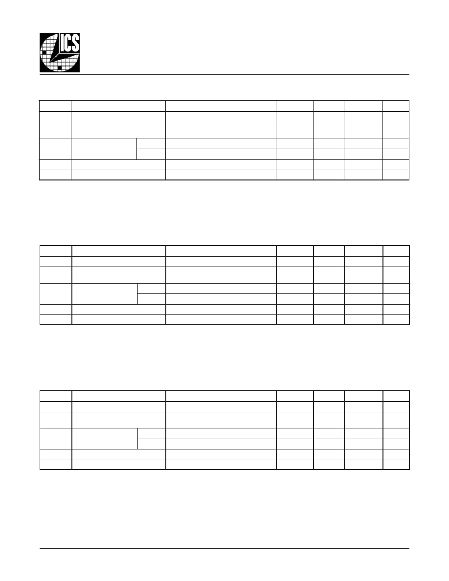
ABLE
4B. AC C
HARACTERISTICS
,
V
DD
= 3.3V±5%, V
DDO
= 2.5V±5%, T
A
= 0∞C
TO
70∞C
l
o
b
m
y
S
r
e
t
e
m
a
r
a
P
s
n
o
i
t
i
d
n
o
C
t
s
e
T
m
u
m
i
n
i
M
l
a
c
i
p
y
T
m
u
m
i
x
a
M
s
t
i
n
U
f
T
U
O
y
c
n
e
u
q
e
r
F
t
u
p
t
u
O
2
1
4
4
.
9
1
0
4
z
H
M
t
)
ÿ
(
t
ij
;
)
m
o
d
n
a
R
(
r
e
t
t
i
J
e
s
a
h
P
S
M
R
1
E
T
O
N
z
H
M
1
-
z
H
k
1
:
e
g
n
a
R
n
o
i
t
a
r
g
e
t
n
I
8
3
.
0
s
p
)
o
(
k
s
t
;
w
e
k
S
t
u
p
t
u
O
3
,
2
E
T
O
N
4
Q
:
0
Q
0
2
s
p
5
Q
:
0
Q
1
˜
=
5
Q
_
L
E
S
_
V
I
D
0
9
s
p
t
R
t
/
F
e
m
i
T
ll
a
F
/
e
s
i
R
t
u
p
t
u
O
%
0
8
o
t
%
0
2
0
0
3
0
0
8
s
p
c
d
o
e
l
c
y
C
y
t
u
D
t
u
p
t
u
O
5
4
5
5
%
.
t
o
l
P
e
s
i
o
N
e
s
a
h
P
e
h
t
o
t
r
e
f
e
r
e
s
a
e
l
P
:
1
E
T
O
N
.
s
n
o
i
t
i
d
n
o
c
d
a
o
l
l
a
u
q
e
h
t
i
w
d
n
a
e
g
a
t
l
o
v
y
l
p
p
u
s
e
m
a
s
e
h
t
t
a
s
t
u
p
t
u
o
n
e
e
w
t
e
b
w
e
k
s
s
a
d
e
n
i
f
e
D
:
2
E
T
O
N
.
s
t
n
i
o
p
s
s
o
r
c
l
a
i
t
n
e
r
e
f
f
i
d
t
u
p
t
u
o
e
h
t
t
a
d
e
r
u
s
a
e
M
.
5
6
d
r
a
d
n
a
t
S
C
E
D
E
J
h
t
i
w
e
c
n
a
d
r
o
c
c
a
n
i
d
e
n
i
f
e
d
s
i
r
e
t
e
m
a
r
a
p
s
i
h
T
:
3
E
T
O
N
T
ABLE
4C. AC C
HARACTERISTICS
,
V
DD
= 3.3V±5%, V
DDO
= 1.8V±0.2V, T
A
= 0∞C
TO
70∞C
l
o
b
m
y
S
r
e
t
e
m
a
r
a
P
s
n
o
i
t
i
d
n
o
C
t
s
e
T
m
u
m
i
n
i
M
l
a
c
i
p
y
T
m
u
m
i
x
a
M
s
t
i
n
U
f
T
U
O
y
c
n
e
u
q
e
r
F
t
u
p
t
u
O
2
1
4
4
.
9
1
0
4
z
H
M
t
)
ÿ
(
t
ij
;
)
m
o
d
n
a
R
(
r
e
t
t
i
J
e
s
a
h
P
S
M
R
1
E
T
O
N
z
H
M
1
-
z
H
k
1
:
e
g
n
a
R
n
o
i
t
a
r
g
e
t
n
I
7
2
.
0
s
p
)
o
(
k
s
t
;
w
e
k
S
t
u
p
t
u
O
3
,
2
E
T
O
N
4
Q
:
0
Q
6
4
s
p
5
Q
:
0
Q
1
˜
=
5
Q
_
L
E
S
_
V
I
D
5
7
1
s
p
t
R
t
/
F
e
m
i
T
ll
a
F
/
e
s
i
R
t
u
p
t
u
O
%
0
8
o
t
%
0
2
0
5
4
0
0
4
1
s
p
c
d
o
e
l
c
y
C
y
t
u
D
t
u
p
t
u
O
4
4
6
5
%
.
t
o
l
P
e
s
i
o
N
e
s
a
h
P
e
h
t
o
t
r
e
f
e
r
e
s
a
e
l
P
:
1
E
T
O
N
.
s
n
o
i
t
i
d
n
o
c
d
a
o
l
l
a
u
q
e
h
t
i
w
d
n
a
e
g
a
t
l
o
v
y
l
p
p
u
s
e
m
a
s
e
h
t
t
a
s
t
u
p
t
u
o
n
e
e
w
t
e
b
w
e
k
s
s
a
d
e
n
i
f
e
D
:
2
E
T
O
N
.
s
t
n
i
o
p
s
s
o
r
c
l
a
i
t
n
e
r
e
f
f
i
d
t
u
p
t
u
o
e
h
t
t
a
d
e
r
u
s
a
e
M
.
5
6
d
r
a
d
n
a
t
S
C
E
D
E
J
h
t
i
w
e
c
n
a
d
r
o
c
c
a
n
i
d
e
n
i
f
e
d
s
i
r
e
t
e
m
a
r
a
p
s
i
h
T
:
3
E
T
O
N

81006AK
www.icst.com/products/hiperclocks.html
REV. A JANUARY 4, 2006
5
Integrated
Circuit
Systems, Inc.
ICS81006
VCXO-
TO
-6 LVCMOS O
UTPUTS
T
ABLE
4D. AC C
HARACTERISTICS
,
V
DD
= V
DDO
= 2.5V±5%, T
A
= 0∞C
TO
70∞C
l
o
b
m
y
S
r
e
t
e
m
a
r
a
P
s
n
o
i
t
i
d
n
o
C
t
s
e
T
m
u
m
i
n
i
M
l
a
c
i
p
y
T
m
u
m
i
x
a
M
s
t
i
n
U
f
T
U
O
y
c
n
e
u
q
e
r
F
t
u
p
t
u
O
2
1
4
4
.
9
1
0
4
z
H
M
t
)
ÿ
(
t
ij
;
)
m
o
d
n
a
R
(
r
e
t
t
i
J
e
s
a
h
P
S
M
R
1
E
T
O
N
z
H
M
1
-
z
H
k
1
:
e
g
n
a
R
n
o
i
t
a
r
g
e
t
n
I
8
2
.
0
s
p
)
o
(
k
s
t
;
w
e
k
S
t
u
p
t
u
O
3
,
2
E
T
O
N
4
Q
:
0
Q
5
2
s
p
5
Q
:
0
Q
1
˜
=
5
Q
_
L
E
S
_
V
I
D
0
0
1
s
p
t
R
t
/
F
e
m
i
T
ll
a
F
/
e
s
i
R
t
u
p
t
u
O
%
0
8
o
t
%
0
2
0
0
3
0
0
8
s
p
c
d
o
e
l
c
y
C
y
t
u
D
t
u
p
t
u
O
5
4
5
5
%
.
t
o
l
P
e
s
i
o
N
e
s
a
h
P
e
h
t
o
t
r
e
f
e
r
e
s
a
e
l
P
:
1
E
T
O
N
.
s
n
o
i
t
i
d
n
o
c
d
a
o
l
l
a
u
q
e
h
t
i
w
d
n
a
e
g
a
t
l
o
v
y
l
p
p
u
s
e
m
a
s
e
h
t
t
a
s
t
u
p
t
u
o
n
e
e
w
t
e
b
w
e
k
s
s
a
d
e
n
i
f
e
D
:
2
E
T
O
N
.
s
t
n
i
o
p
s
s
o
r
c
l
a
i
t
n
e
r
e
f
f
i
d
t
u
p
t
u
o
e
h
t
t
a
d
e
r
u
s
a
e
M
.
5
6
d
r
a
d
n
a
t
S
C
E
D
E
J
h
t
i
w
e
c
n
a
d
r
o
c
c
a
n
i
d
e
n
i
f
e
d
s
i
r
e
t
e
m
a
r
a
p
s
i
h
T
:
3
E
T
O
N
T
ABLE
4E. AC C
HARACTERISTICS
,
V
DD
= 2.5V±5%, V
DDO
= 1.8V±0.2V, T
A
= 0∞C
TO
70∞C
l
o
b
m
y
S
r
e
t
e
m
a
r
a
P
s
n
o
i
t
i
d
n
o
C
t
s
e
T
m
u
m
i
n
i
M
l
a
c
i
p
y
T
m
u
m
i
x
a
M
s
t
i
n
U
f
T
U
O
y
c
n
e
u
q
e
r
F
t
u
p
t
u
O
2
1
4
4
.
9
1
0
4
z
H
M
t
)
ÿ
(
t
ij
;
)
m
o
d
n
a
R
(
r
e
t
t
i
J
e
s
a
h
P
S
M
R
1
E
T
O
N
z
H
M
1
-
z
H
k
1
:
e
g
n
a
R
n
o
i
t
a
r
g
e
t
n
I
6
2
.
0
s
p
)
o
(
k
s
t
;
w
e
k
S
t
u
p
t
u
O
3
,
2
E
T
O
N
4
Q
:
0
Q
0
4
s
p
5
Q
:
0
Q
1
˜
=
5
Q
_
L
E
S
_
V
I
D
5
7
1
s
p
t
R
t
/
F
e
m
i
T
ll
a
F
/
e
s
i
R
t
u
p
t
u
O
%
0
8
o
t
%
0
2
0
5
4
0
0
4
1
s
p
c
d
o
e
l
c
y
C
y
t
u
D
t
u
p
t
u
O
0
4
0
6
%
.
t
o
l
P
e
s
i
o
N
e
s
a
h
P
e
h
t
o
t
r
e
f
e
r
e
s
a
e
l
P
:
1
E
T
O
N
.
s
n
o
i
t
i
d
n
o
c
d
a
o
l
l
a
u
q
e
h
t
i
w
d
n
a
e
g
a
t
l
o
v
y
l
p
p
u
s
e
m
a
s
e
h
t
t
a
s
t
u
p
t
u
o
n
e
e
w
t
e
b
w
e
k
s
s
a
d
e
n
i
f
e
D
:
2
E
T
O
N
.
s
t
n
i
o
p
s
s
o
r
c
l
a
i
t
n
e
r
e
f
f
i
d
t
u
p
t
u
o
e
h
t
t
a
d
e
r
u
s
a
e
M
.
5
6
d
r
a
d
n
a
t
S
C
E
D
E
J
h
t
i
w
e
c
n
a
d
r
o
c
c
a
n
i
d
e
n
i
f
e
d
s
i
r
e
t
e
m
a
r
a
p
s
i
h
T
:
3
E
T
O
N
81006AK
www.icst.com/products/hiperclocks.html
REV. A JANUARY 4, 2006
6
Integrated
Circuit
Systems, Inc.
ICS81006
VCXO-
TO
-6 LVCMOS O
UTPUTS
T
YPICAL
P
HASE
N
OISE
AT
19.44MH
Z
@ 3.3V C
ORE
/3.3V O
UTPUT
19.44MHz
RMS Phase Jitter (Random)
1kHz to 1MHz = 0.35ps (typical)
O
FFSET
F
REQUENCY
(H
Z
)
dBc
Hz
N
OISE
P
OWER
0
-10
-20
-30
-40
-50
-60
-70
-80
-90
-100
-110
-120
-130
-140
-150
-160
-170
-180
-190
100
1k
10k
100k
1M

81006AK
www.icst.com/products/hiperclocks.html
REV. A JANUARY 4, 2006
7
Integrated
Circuit
Systems, Inc.
ICS81006
VCXO-
TO
-6 LVCMOS O
UTPUTS
Phase Noise Mask
Offset Frequency
f
1
f
2
Phase Noise Plot
RMS Jitter = Area Under the Masked Phase Noise Plot
Noise P
o
w
er
P
ARAMETER
M
EASUREMENT
I
NFORMATION
SCOPE
Qx
LVCMOS
3.3V C
ORE
/1.8V O
UTPUT
L
OAD
AC T
EST
C
IRCUIT
2.4V±0.065V
V
DDO
-0.9V±0.1V
V
DD
0.9V±0.1V
SCOPE
Qx
LVCMOS
3.3V C
ORE
/2.5V O
UTPUT
L
OAD
AC T
EST
C
IRCUIT
2.05V±5%
V
DDO
-1.25V±5%
V
DD
1.25V±5%
3.3V C
ORE
/3.3V O
UTPUT
L
OAD
AC T
EST
C
IRCUIT
SCOPE
Qx
LVCMOS
1.65V±5%
-1.65V±5%
2.5V C
ORE
/2.5V O
UTPUT
L
OAD
AC T
EST
C
IRCUIT
2.5 C
ORE
/1.8V O
UTPUT
L
OAD
AC T
EST
C
IRCUIT
RMS P
HASE
J
ITTER
SCOPE
Qx
LVCMOS
1.6V±0.025V
V
DDO
-0.9V±0.1V
V
DD
0.9V±0.1V
V
DD
,
V
DDO
GND
GND
GND
GND
SCOPE
Qx
LVCMOS
1.25V±5%
-1.25V±5%
V
DD
,
V
DDO
GND

81006AK
www.icst.com/products/hiperclocks.html
REV. A JANUARY 4, 2006
8
Integrated
Circuit
Systems, Inc.
ICS81006
VCXO-
TO
-6 LVCMOS O
UTPUTS
O
UTPUT
R
ISE
/F
ALL
T
IME
O
UTPUT
S
KEW
Clock
Outputs
20%
80%
80%
20%
t
R
t
F
t
PERIOD
t
PW
t
PERIOD
odc =
V
DD
2
x 100%
t
PW
Q0:Q5
O
UTPUT
D
UTY
C
YCLE
/P
ULSE
W
IDTH
/P
ERIOD
t
sk(o)
V
DDO
2
V
DDO
2
Qy
Qx
81006AK
www.icst.com/products/hiperclocks.html
REV. A JANUARY 4, 2006
9
Integrated
Circuit
Systems, Inc.
ICS81006
VCXO-
TO
-6 LVCMOS O
UTPUTS
Oscillator
A
PPLICATION
I
NFORMATION
F
IGURE
1: VCXO O
SCILLATOR
C
IRCUIT
V
C
C
V
C
S 1
C
L1
C
S 2
C
L2
C
V
XTAL
VCXO (Internal)
Optional
Control Voltage
T
ABLE
5. E
XAMPLE
C
RYSTAL
P
ARAMETERS
l
o
b
m
y
S
r
e
t
e
m
a
r
a
P
s
n
o
i
t
i
d
n
o
C
t
s
e
T
m
u
m
i
n
i
M
l
a
c
i
p
y
T
m
u
m
i
x
a
M
s
t
i
n
U
f
N
y
c
n
e
u
q
e
r
F
l
a
n
i
m
o
N
4
4
.
9
1
z
H
M
f
T
e
c
n
a
r
e
l
o
T
y
c
n
e
u
q
e
r
F
0
2
±
m
p
p
f
S
y
t
il
i
b
a
t
S
y
c
n
e
u
q
e
r
F
0
2
±
m
p
p
e
g
n
a
R
e
r
u
t
a
r
e
p
m
e
T
g
n
i
t
a
r
e
p
O
0
0
7
C
∞
C
L
e
c
n
a
t
i
c
a
p
a
C
d
a
o
L
2
1
F
p
C
O
e
c
n
a
t
i
c
a
p
a
C
t
n
u
h
S
4
F
p
C
,
0
C
1
o
i
t
a
R
y
t
il
i
b
a
ll
u
P
0
2
2
0
4
2
R
S
E
e
c
n
a
t
s
i
s
e
R
s
e
i
r
e
S
t
n
e
l
a
v
i
u
q
E
0
2
l
e
v
e
L
e
v
i
r
D
1
W
m
C
∞
5
2
@
g
n
i
g
A
r
a
e
y
r
e
p
3
±
m
p
p
n
o
i
t
a
r
e
p
O
f
o
e
d
o
M
l
a
t
n
e
m
a
d
n
u
F
VCXO C
RYSTAL
S
ELECTION
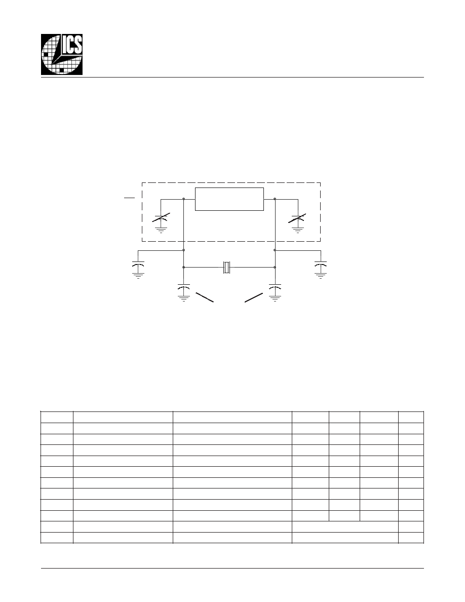
Choosing a crystal with the correct characteristics is one of
the most critical steps in using a Voltage Controlled Crystal
Oscillator (VCXO). The crystal parameters affect the tuning
V
C
Control voltage used to tune frequency
C
V
Varactor capacitance, varies due to the change in
control voltage
range and accuracy of a VCXO. Below are the key variables
and an example of using the crystal parameters to calculate
the tuning range of the VCXO.
C
L1,
C
L2
Load tuning capacitance used for fine tuning or
centering nominal frequency
C
S1,
C
S2
Stray Capacitance caused by pads, vias, and other
board parasitics

81006AK
www.icst.com/products/hiperclocks.html
REV. A JANUARY 4, 2006
10
Integrated
Circuit
Systems, Inc.
ICS81006
VCXO-
TO
-6 LVCMOS O
UTPUTS
l
o
b
m
y
S
r
e
t
e
m
a
r
a
P
s
n
o
i
t
i
d
n
o
C
t
s
e
T
m
u
m
i
n
i
M
l
a
c
i
p
y
T
m
u
m
i
x
a
M
s
t
i
n
U
C
W
O
L
_
V
e
c
n
a
t
i
c
a
p
a
C
r
o
t
c
a
r
a
V
w
o
L
V
C
V
0
=
4
.
5
1
F
p
C
H
G
I
H
_
V
e
c
n
a
t
i
c
a
p
a
C
r
o
t
c
a
r
a
V
h
g
i
H
V
C
V
3
.
3
=
6
.
9
2
F
p
T
ABLE
6. V
ARACTOR
P
ARAMETERS
F
ORMULAS
(
) (
)
(
) (
)
Low
V
S
L
Low
V
S
L
Low
V
S
L
Low
V
S
L
Low
C
C
C
C
C
C
C
C
C
C
C
C
C
_
2
2
_
1
1
_
2
2
_
1
1
+
+
+
+
+
+
+
+
+
=
(
) (
)
(
) (
)
High
V
S
L
High
V
S
L
High
V
S
L
High
V
S
L
High
C
C
C
C
C
C
C
C
C
C
C
C
C
_
2
2
_
1
1
_
2
2
_
1
1
+
+
+
+
+
+
+
+
+
=
6
0
1
0
0
1
0
10
1
2
1
1
2
1
)
(
+
-
+
=
C
C
C
C
C
C
C
C
TPR
Range
Pull
Total
High
Low
∑ C
Low
is the effective capacitance due to the low varactor capacitance, load capacitance and stray capacitance.
C
Low
determines the high frequency component on the TPR.
∑ C
High
is the effective capacitance due to the high varactor capacitance, load capacitance and stray capacitance.
C
High
determines the low frequency component on the TPR.
Absolute Pull Range (APR) = Total Pull Range ≠ (Frequency Tolerance + Frequency Stability + Aging)
E
XAMPLE
C
ALCULATIONS
Using the tables and figures above, we can now calculate the
TPR and APR of the VCXO using the example crystal
parameters. For the numerical example below there were some
assumptions made. First, the stray capacitance (C
S1
, C
S2
), which
is all the excess capacitance due to board parasitic, is 4pF.
Second, the expected lifetime of the project is 5 years; hence
the inaccuracy due to aging is ±15ppm. Third, though many
boards will not require load tuning capacitors (C
L1
, C
L2
), it is
recommended for long-term consistent performance of the
system that two tuning capacitor pads be placed into every
design. Typical values for the load tuning capacitors will range
from 0 to 4pF.
(
) (
)
(
) (
)
pf
pf
pf
pf
pf
pf
pf
pf
pf
C
Low
7
.
9
4
.
15
4
0
4
.
15
4
0
4
.
15
4
0
4
.
15
4
0
=
+
+
+
+
+
+
+
+
+
=
(
) (
)
(
) (
)
pf
pf
pf
pf
pf
pf
pf
pf
pf
C
High
8
.
16
6
.
29
4
0
6
.
29
4
0
6
.
29
4
0
6
.
29
4
0
=
+
+
+
+
+
+
+
+
+
=
ppm
pF
pF
pF
pF
TPR
5
.
226
10
4
8
.
16
1
220
2
1
4
7
.
9
1
220
2
1
6
=
+
-
+
=
TPR = ±113.25ppm
APR = 113.25ppm ≠ (20ppm + 20ppm + 15ppm) = ±58.25ppm
The example above will ensure a total pull range of
±113.25 ppm with an APR of ±58.25ppm. Many times, board
designers may select their own crystal based on their
application. If the application requires a tighter APR, a crystal
with better pullability (C0/C1 ratio) can be used. Also, with the
equations above, one can vary the frequency tolerance,
temperature stability, and aging or shunt capacitance to achieve
the required pullability.

81006AK
www.icst.com/products/hiperclocks.html
REV. A JANUARY 4, 2006
11
Integrated
Circuit
Systems, Inc.
ICS81006
VCXO-
TO
-6 LVCMOS O
UTPUTS
S
CHEMATIC
E
XAMPLE
Figure 2
shows an example of ICS81006 application sche-
matic. The decoupling capacitors should be located as close
as possible to the power pin. For the LVCMOS 20
output
drivers, series termination example is shown in the sche-
matic. Additional termination approaches are shown in the
LVCMOS Termination Application Note.
F
IGURE
2. ICS81006 S
CHEMATIC
E
XAMPLE
I
NPUTS
:
C
ONTROL
P
INS
:
All control pins have internal pull-ups or pull-downs; additional
resistance is not required but can be added for additional
protection. A 1k
resistor can be used. The VC pin can not be
floated.
R
ECOMMENDATIONS
FOR
U
NUSED
I
NPUT
AND
O
UTPUT
P
INS
O
UTPUTS
:
LVCMOS O
UTPUT
:
All unused LVCMOS output can be left floating. We
recommend that there is no trace attached.
C2
SPARE
R5
1K
VC = 0V to VDD
VDD
C1
SPARE
U1
81006
2
3
4
5
6
7
8
9
11
12
13
14
17
18
19
20
10
16
15
1
XTAL_OUT
VDD
VC
DIV_SEL_Q5
OE
1
GN
D
Q5
VD
D
O
GND
Q3
VDDO
Q2
VD
D
O
Q0
GN
D
OE
0
Q4
Q
1
GND
XTAL_IN
Zo = 50
(U1-13)
C3
0.1uF
Unused outputs can be left floating. There should be
no trace attached to unused outputs. Device
characterized and specification limits set with all
outputs terminated.
C6
0.1uF
C5
0.1uF
C7
10uf
Pull-up
example
(U1-9)
R4
1K
Quartz crystal should be
placed as close to the
device as possible.
VDDO
Pull-down
example
VDD
R3
1K
VDDO
R1
30
VDD
R2
30
VC
C4
0.1uF
XTAL
(U1-17)
Zo = 50
VDD
(U1-3)

81006AK
www.icst.com/products/hiperclocks.html
REV. A JANUARY 4, 2006
12
Integrated
Circuit
Systems, Inc.
ICS81006
VCXO-
TO
-6 LVCMOS O
UTPUTS
R
ELIABILITY
I
NFORMATION
T
RANSISTOR
C
OUNT
The transistor count for ICS81006 is: 983
T
ABLE
7.
JA
VS
. A
IR
F
LOW
T
ABLE
FOR
20 L
EAD
VFQFN
JA
by Velocity (Meters Per Second)
0
1
2.5
Single-Layer PCB, JEDEC Standard Test Boards
141.7∞C/W
126.0∞C/W
116.9∞C/W
Multi-Layer PCB, JEDEC Standard Test Boards
38.5∞C/W
35.0∞C/W
33.4∞C/W
NOTE: Most modern PCB designs use multi-layered boards. The data in the second row pertains to most designs.

81006AK
www.icst.com/products/hiperclocks.html
REV. A JANUARY 4, 2006
13
Integrated
Circuit
Systems, Inc.
ICS81006
VCXO-
TO
-6 LVCMOS O
UTPUTS
P
ACKAGE
O
UTLINE
- K S
UFFIX
FOR
20 L
EAD
VFQFN
T
ABLE
8. P
ACKAGE
D
IMENSIONS
Reference Document: JEDEC Publication 95, MO-220
N
O
I
T
A
I
R
A
V
C
E
D
E
J
S
R
E
T
E
M
I
L
L
I
M
N
I
S
N
O
I
S
N
E
M
I
D
L
L
A
L
O
B
M
Y
S
M
U
M
I
N
I
M
M
U
M
I
X
A
M
N
0
2
A
0
8
.
0
0
.
1
1
A
0
5
0
.
0
3
A
e
c
n
e
r
e
f
e
R
5
2
.
0
b
8
1
.
0
0
3
.
0
e
C
I
S
A
B
0
5
.
0
N
D
5
N
E
5
D
0
.
4
2
D
5
7
.
0
0
8
.
2
E
0
.
4
2
E
5
7
.
0
0
8
.
2
L
5
3
.
0
5
7
.
0

81006AK
www.icst.com/products/hiperclocks.html
REV. A JANUARY 4, 2006
14
Integrated
Circuit
Systems, Inc.
ICS81006
VCXO-
TO
-6 LVCMOS O
UTPUTS
T
ABLE
9. O
RDERING
I
NFORMATION
While the information presented herein has been checked for both accuracy and reliability, Integrated Circuit Systems, Incorporated (ICS) assumes no responsibility for either its use
or for infringement of any patents or other rights of third parties, which would result from its use. No other circuits, patents, or licenses are implied. This product is intended for use
in normal commercial applications. Any other applications such as those requiring extended temperature range, high reliability, or other extraordinary environmental requirements are
not recommended without additional processing by ICS. ICS reserves the right to change any circuitry or specifications without notice. ICS does not authorize or warrant any ICS
product for use in life support devices or critical medical instruments.
The aforementioned trademark, HiPerClockS is a trademark of Integrated Circuit Systems, Inc. or its subsidiaries in the United States and/or other countries.
r
e
b
m
u
N
r
e
d
r
O
/
t
r
a
P
g
n
i
k
r
a
M
e
g
a
k
c
a
P
g
n
i
g
a
k
c
a
P
g
n
i
p
p
i
h
S
e
r
u
t
a
r
e
p
m
e
T
K
A
6
0
0
1
8
S
C
I
A
6
0
0
1
8
N
F
Q
F
V
d
a
e
l
0
2
e
b
u
t
C
∞
0
7
o
t
C
∞
0
T
K
A
6
0
0
1
8
S
C
I
A
6
0
0
1
8
N
F
Q
F
V
d
a
e
l
0
2
l
e
e
r
&
e
p
a
t
0
0
5
2
C
∞
0
7
o
t
C
∞
0
F
L
K
A
6
0
0
1
8
S
C
I
D
B
T
N
F
Q
F
V
"
e
e
r
F
-
d
a
e
L
"
d
a
e
l
0
2
e
b
u
t
C
∞
0
7
o
t
C
∞
0
T
F
L
K
A
6
0
0
1
8
S
C
I
D
B
T
N
F
Q
F
V
"
e
e
r
F
-
d
a
e
L
"
d
a
e
l
0
2
l
e
e
r
&
e
p
a
t
0
0
5
2
C
∞
0
7
o
t
C
∞
0
.
t
n
a
il
p
m
o
c
S
H
o
R
e
r
a
d
n
a
n
o
i
t
a
r
u
g
i
f
n
o
c
e
e
r
F
-
b
P
e
h
t
e
r
a
r
e
b
m
u
n
t
r
a
p
e
h
t
o
t
x
i
f
f
u
s
"
F
L
"
n
a
h
t
i
w
d
e
r
e
d
r
o
e
r
a
t
a
h
t
s
t
r
a
P
:
E
T
O
N